Compound Semiconductor IC Symposium A HighGain LowNoise 6
![References [1] D. Alldred et al, CSICS 2006 [2] S. P. Voinigescu et al, References [1] D. Alldred et al, CSICS 2006 [2] S. P. Voinigescu et al,](https://slidetodoc.com/presentation_image/668b949bd894a1086b84015060323c72/image-21.jpg)
- Slides: 21

Compound Semiconductor IC Symposium A High-Gain, Low-Noise, +6 d. Bm PA in 90 nm CMOS for 60 -GHz Radio Mehdi Khanpour+, Sorin Voinigescu+, M. T. Yang* +University of Toronto, *TSMC October 2007 Mehdi Khanpour

Outline • • • Motivation 60 -GHz Radio PA schematic Fabrication Measurement results Conclusion October 2007 Mehdi Khanpour 2

Motivation • 60 -GHz Band (57 -64 GHz) – Large bandwidth and limited propagation – High data rate (4+Gbps), short range – Personal Area Networks, Wireless HDTV • CMOS alternative – lower power – higher integration and lower cost October 2007 Mehdi Khanpour 3

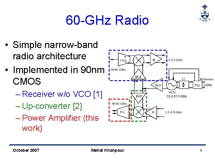
60 -GHz Radio • Simple narrow-band radio architecture • Implemented in 90 nm CMOS – Receiver w/o VCO [1] – Up-converter [2] – Power Amplifier (this work) October 2007 Mehdi Khanpour 4

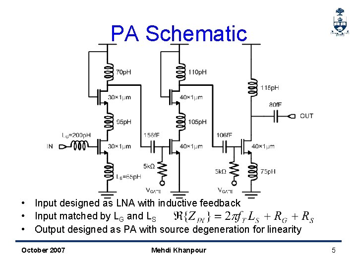
PA Schematic • Input designed as LNA with inductive feedback • Input matched by LG and LS • Output designed as PA with source degeneration for linearity October 2007 Mehdi Khanpour 5

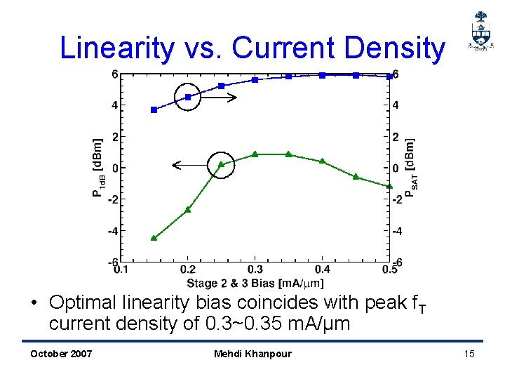
PA Design • Stage 1 biased at 0. 2 m. A/μm and sized for simultaneous noise and input impedance matching • Stage 2 and 3 biased at 0. 3 m. A/μm for linearity • Output stage sized for PSAT = 6. 5 d. Bm with Inductive degeneration for linearity • Inductors and interconnects modeled using ASITIC October 2007 Mehdi Khanpour 6

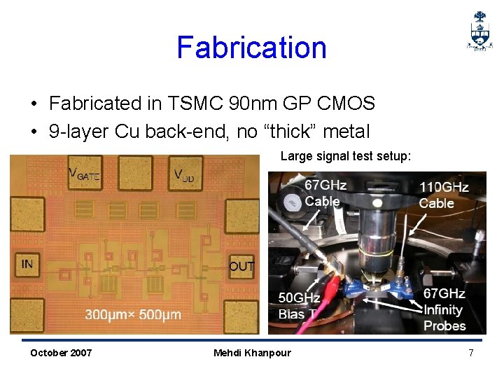
Fabrication • Fabricated in TSMC 90 nm GP CMOS • 9 -layer Cu back-end, no “thick” metal Large signal test setup: 67 GHz Cable 300μm× 500μm October 2007 50 GHz Bias T Mehdi Khanpour 110 GHz Cable 67 GHz Infinity Probes 7

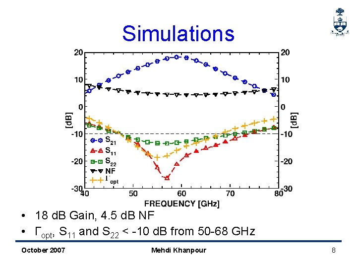
Simulations • 18 d. B Gain, 4. 5 d. B NF • Γopt, S 11 and S 22 < -10 d. B from 50 -68 GHz October 2007 Mehdi Khanpour 8

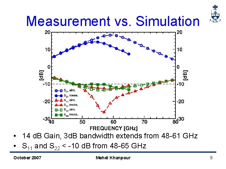
Measurement vs. Simulation • 14 d. B Gain, 3 d. B bandwidth extends from 48 -61 GHz • S 11 and S 22 < -10 d. B from 48 -65 GHz October 2007 Mehdi Khanpour 9

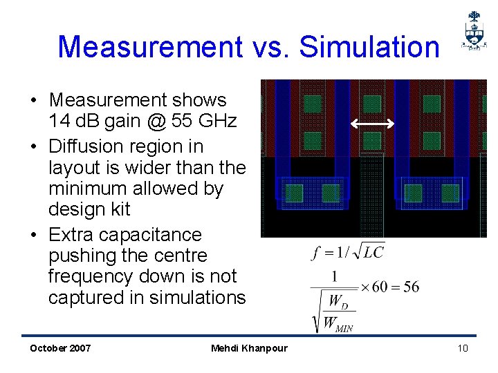
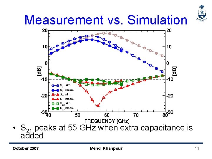
Measurement vs. Simulation • Measurement shows 14 d. B gain @ 55 GHz • Diffusion region in layout is wider than the minimum allowed by design kit • Extra capacitance pushing the centre frequency down is not captured in simulations October 2007 Mehdi Khanpour 10

Measurement vs. Simulation • S 21 peaks at 55 GHz when extra capacitance is added October 2007 Mehdi Khanpour 11

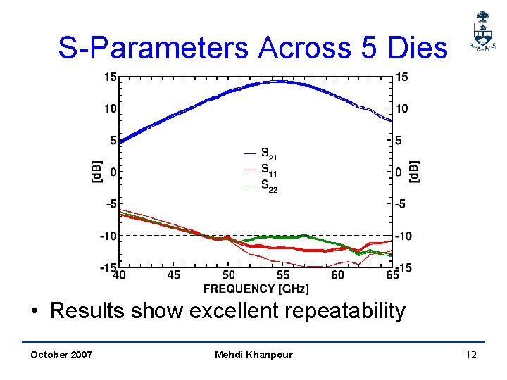
S-Parameters Across 5 Dies • Results show excellent repeatability October 2007 Mehdi Khanpour 12

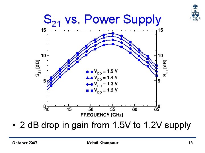
S 21 vs. Power Supply • 2 d. B drop in gain from 1. 5 V to 1. 2 V supply October 2007 Mehdi Khanpour 13

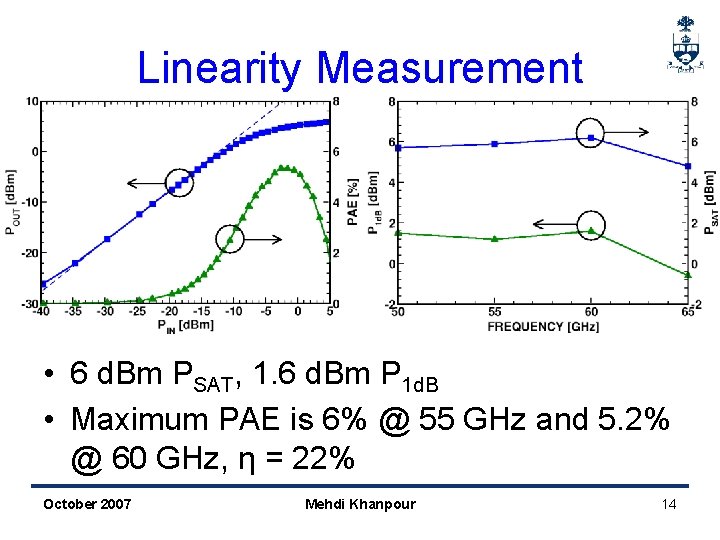
Linearity Measurement • 6 d. Bm PSAT, 1. 6 d. Bm P 1 d. B • Maximum PAE is 6% @ 55 GHz and 5. 2% @ 60 GHz, η = 22% October 2007 Mehdi Khanpour 14

Linearity vs. Current Density • Optimal linearity bias coincides with peak f. T current density of 0. 3~0. 35 m. A/μm October 2007 Mehdi Khanpour 15

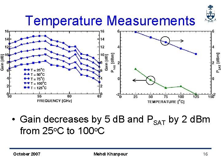
Temperature Measurements • Gain decreases by 5 d. B and PSAT by 2 d. Bm from 25 o. C to 100 o. C October 2007 Mehdi Khanpour 16

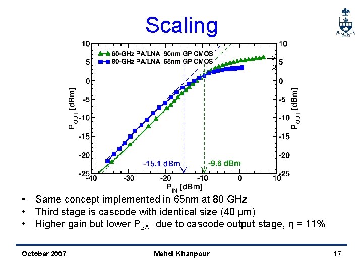
Scaling • Same concept implemented in 65 nm at 80 GHz • Third stage is cascode with identical size (40 μm) • Higher gain but lower PSAT due to cascode output stage, η = 11% October 2007 Mehdi Khanpour 17

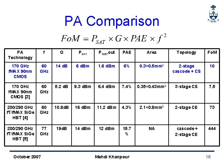
PA Comparison PA Technology f G PSAT P 1 d. B, out PAE Area Topology Fo. M 170 GHz f. MAX 90 nm CMOS 60 GHz 14 d. B 6 d. Bm 1. 6 d. Bm 6% 0. 3× 0. 5 mm 2 2 -stage cascode + CS 10 170 GHz f. MAX 90 nm CMOS [3] 60 GHz 5. 2 d. B 9. 3 d. Bm 6. 4 d. Bm 7. 4% 0. 35× 0. 43 mm 2 3 -stage CS 7. 5 200/290 GHz f. T/f. MAX Si. Ge HBT [4] 60 GHz 10. 8 d. B 16 d. Bm 11. 2 d. Bm 4. 3% 2. 1× 0. 8 mm 2 2 -stage CE 73 200/290 GHz f. T/f. MAX Si. Ge HBT [5] 77 GHz 19 d. B 14 d. Bm 12 d. Bm 15. 7 % NA cascode + 2 -stage CE 444 October 2007 Mehdi Khanpour 18

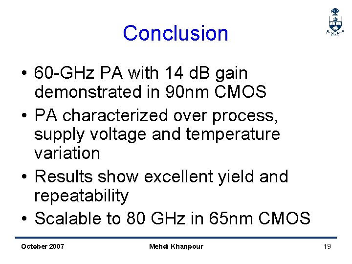
Conclusion • 60 -GHz PA with 14 d. B gain demonstrated in 90 nm CMOS • PA characterized over process, supply voltage and temperature variation • Results show excellent yield and repeatability • Scalable to 80 GHz in 65 nm CMOS October 2007 Mehdi Khanpour 19

Acknowledgment • Jaro Pristupa and CMC for CAD tools and support • OIT and CFI for equipment grants • TSMC for facilitating the technology access October 2007 Mehdi Khanpour 20
![References 1 D Alldred et al CSICS 2006 2 S P Voinigescu et al References [1] D. Alldred et al, CSICS 2006 [2] S. P. Voinigescu et al,](https://slidetodoc.com/presentation_image/668b949bd894a1086b84015060323c72/image-21.jpg)
References [1] D. Alldred et al, CSICS 2006 [2] S. P. Voinigescu et al, ISCAS 2007 [3] T. Yao et al. RFIC-Symp 2006 [4] B. Floyd et al, ISSCC 2004 [5] S. T. Nicolson et al, IMS 2007 October 2007 Mehdi Khanpour 21