Complete Design Methodology of A Massively Parallel and



![Memristors [Chua] 10/29/2020 [Kuekes] 4 Memristors [Chua] 10/29/2020 [Kuekes] 4](https://slidetodoc.com/presentation_image/1d74422753b663503afbd4c8a62e83db/image-4.jpg)













![Power Consumption Sources of Memristor-Nanowire Design [Strukov] • 10/29/2020 45 Power Consumption Sources of Memristor-Nanowire Design [Strukov] • 10/29/2020 45](https://slidetodoc.com/presentation_image/1d74422753b663503afbd4c8a62e83db/image-45.jpg)













- Slides: 71

Complete Design Methodology of A Massively Parallel and Pipelined Memristive Stateful IMPLY Logic Based Reconfigurable Architecture Kamela C. Rahman Dissertation Committee: Marek A. Perkowski, Chair Dan Hammerstrom Xiaoyu Song Rolf Koenenkamp, GO Rep 10/29/2020 1

Motivation üBiologically Inspired Associative Memory Based Modeling üMassively Parallel and Pipelined Architecture üNeuromorphic Nanoscale Circuits and Devices üMethodology Development for non-von-Neumann architectures 10/29/2020 2

Research Groundwork üEuclidean Distance üEvaluation of AM Based Algorithms üMemristor Research and memristive FPGA 10/29/2020 3
![Memristors Chua 10292020 Kuekes 4 Memristors [Chua] 10/29/2020 [Kuekes] 4](https://slidetodoc.com/presentation_image/1d74422753b663503afbd4c8a62e83db/image-4.jpg)
Memristors [Chua] 10/29/2020 [Kuekes] 4

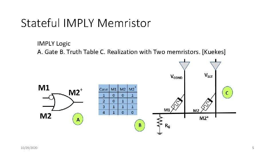
Stateful IMPLY Memristor IMPLY Logic A. Gate B. Truth Table C. Realization with Two memristors. [Kuekes] 10/29/2020 5

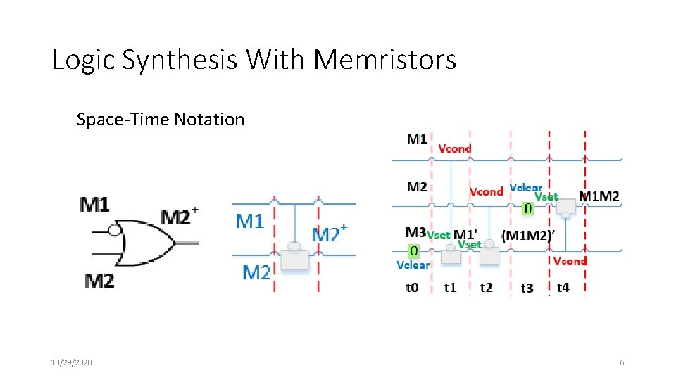
Logic Synthesis With Memristors Space-Time Notation 10/29/2020 6

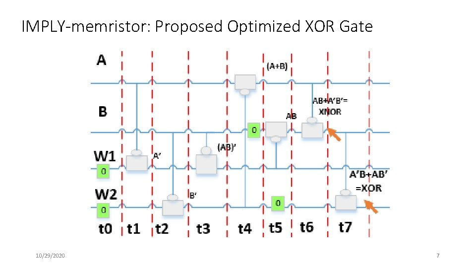
IMPLY-memristor: Proposed Optimized XOR Gate 10/29/2020 7

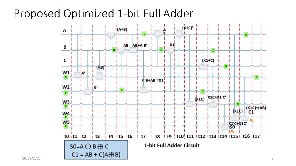
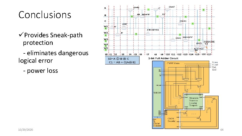
Proposed Optimized 1 -bit Full Adder 10/29/2020 8

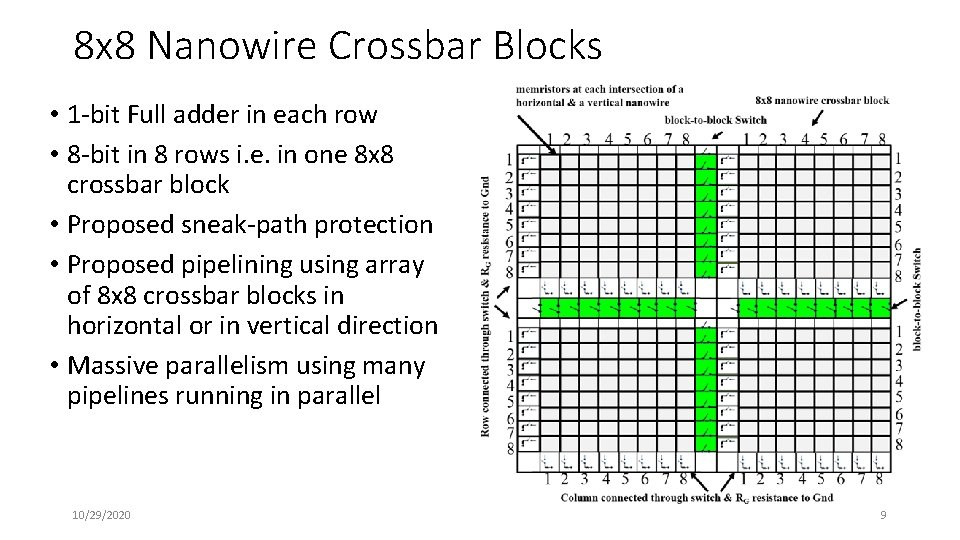
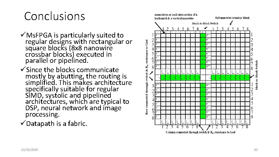
8 x 8 Nanowire Crossbar Blocks • 1 -bit Full adder in each row • 8 -bit in 8 rows i. e. in one 8 x 8 crossbar block • Proposed sneak-path protection • Proposed pipelining using array of 8 x 8 crossbar blocks in horizontal or in vertical direction • Massive parallelism using many pipelines running in parallel 10/29/2020 9

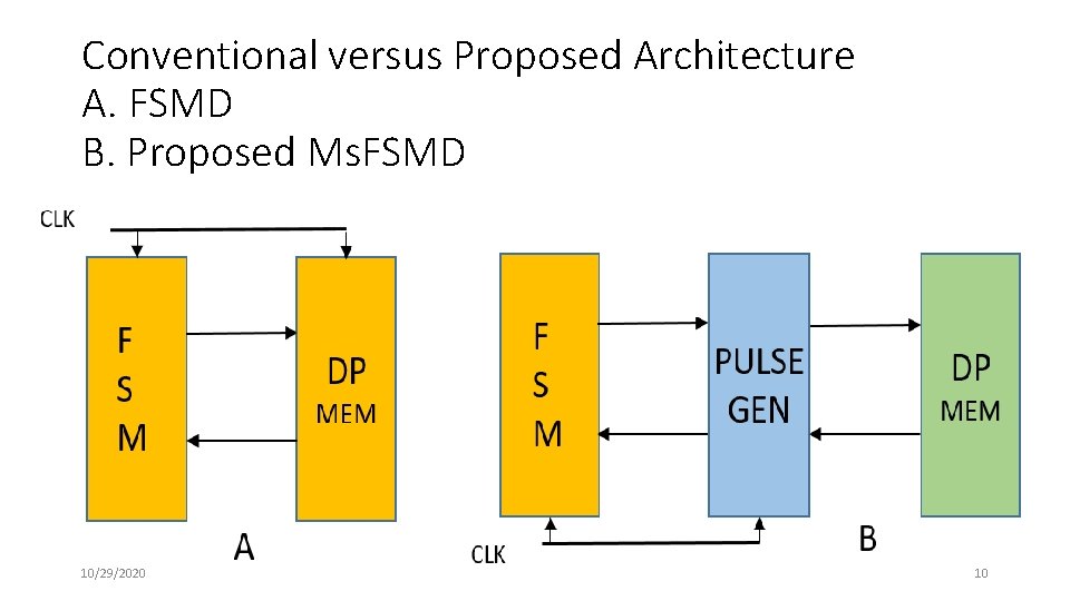
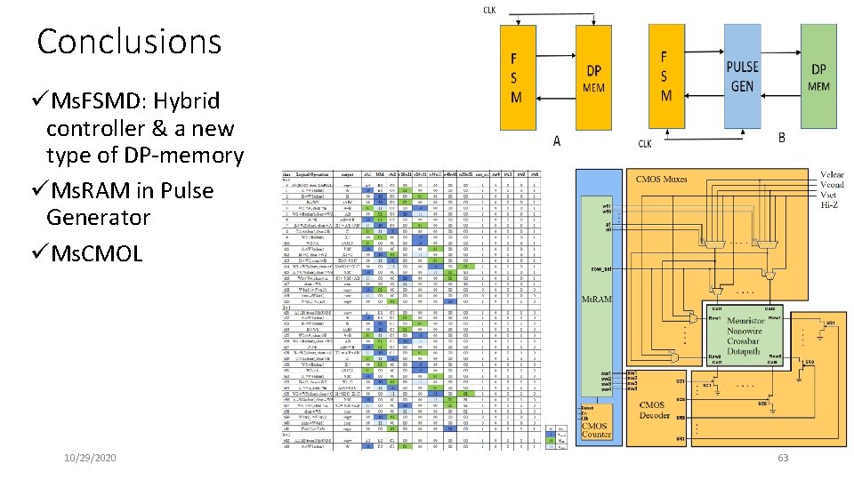
Conventional versus Proposed Architecture A. FSMD B. Proposed Ms. FSMD 10/29/2020 10

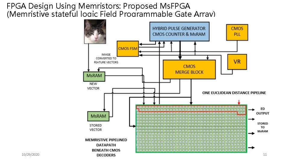
FPGA Design Using Memristors: Proposed Ms. FPGA (Memristive stateful logic Field Programmable Gate Array) 10/29/2020 11

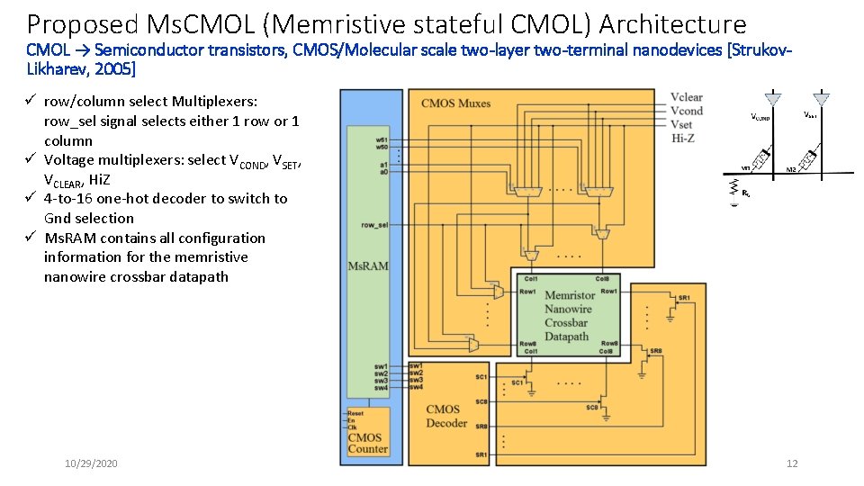
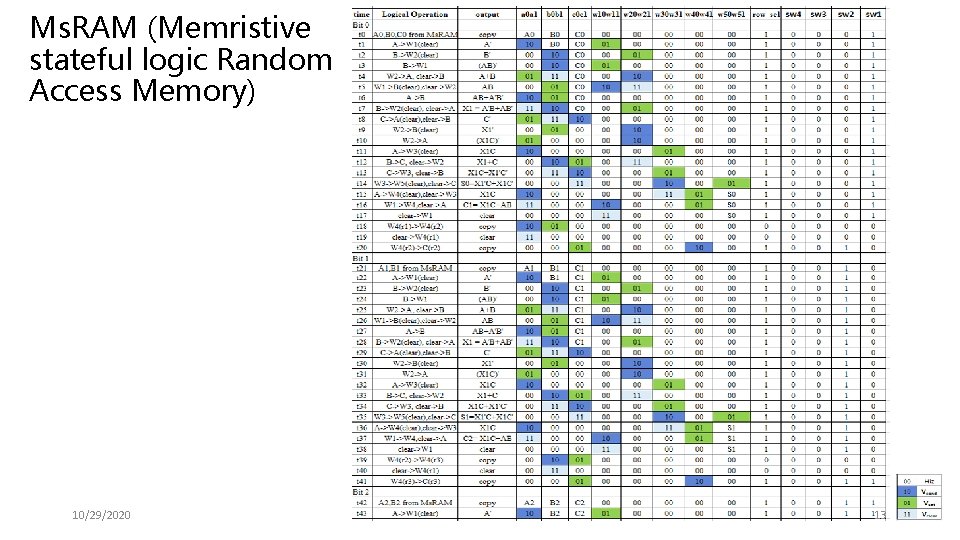
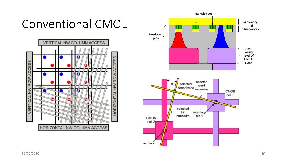
Proposed Ms. CMOL (Memristive stateful CMOL) Architecture CMOL → Semiconductor transistors, CMOS/Molecular scale two-layer two-terminal nanodevices [Strukov. Likharev, 2005] ü row/column select Multiplexers: row_sel signal selects either 1 row or 1 column ü Voltage multiplexers: select VCOND, VSET, VCLEAR, Hi. Z ü 4 -to-16 one-hot decoder to switch to Gnd selection ü Ms. RAM contains all configuration information for the memristive nanowire crossbar datapath 10/29/2020 12

Ms. RAM (Memristive stateful logic Random Access Memory) 10/29/2020 13

What is special about Ms. FPGA? ü Published FPGA in nanotechnologies by Strukov & Likharev, S. Kang, Williams R. S. , & mr. FPGA by Cong. 10/29/2020 14

What is special about Ms. FPGA? Comparison with other published memristive FPGA üi. Mem. Comp NVM logic architecture [Li et al. (2015) @Nature Scientific reports] 10/29/2020 15

Issue with Sneak-Path Current (a) Current Flows Through Target Cells (b) Current Flows Through Undesired Paths. [99] 10/29/2020 16

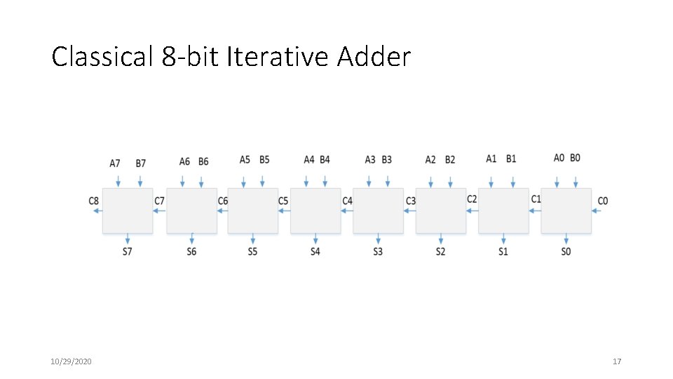
Classical 8 -bit Iterative Adder 10/29/2020 17

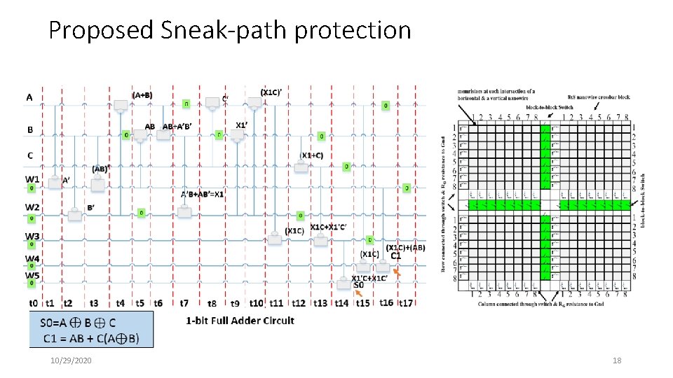
Proposed Sneak-path protection 10/29/2020 18

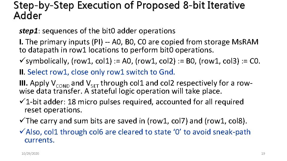
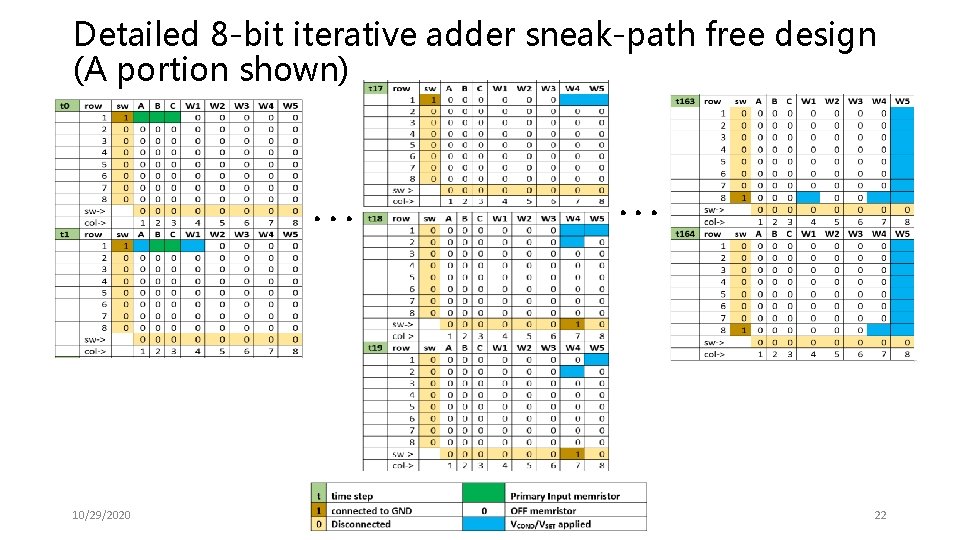
Step-by-Step Execution of Proposed 8 -bit Iterative Adder step 1: sequences of the bit 0 adder operations I. The primary inputs (PI) -- A 0, B 0, C 0 are copied from storage Ms. RAM to datapath in row 1 locations to perform bit 0 operations. üsymbolically, (row 1, col 1) : = A 0, (row 1, col 2) : = B 0, (row 1, col 3) : = C 0. II. Select row 1, close only row 1 switch to Gnd. III. Apply VCOND and VSET through col 1 and col 2 respectively for a rowwise data transfer. A stateful logic operation will take place. ü 1 -bit adder: 18 micro pulses required, accounted for all required reset operations. üThe carry and sum bits are saved in (row 1, col 7) and (row 1, col 8). üAlso, col 1 through col 6 are cleared to state ‘ 0’ to avoid sneak-path currents. 10/29/2020 19

Step-by-Step Execution of Proposed 8 -bit Iterative Adder step 2: Copying of the carry bit from the current row to the next row. Here it is demonstrated for (row 1, col 7) to (row 2, col 7). I. Disconnect row 1 from Gnd. Select col 7, close only col 7 switch to Gnd. II. Apply VCOND to (row 1, col 7) and VSET to (row 2, col 7) for a column-wise data transfer. Stateful logic is transferred from (row 1, col 7) to (row 2, col 7). III. Apply VCLEAR to (row 1, col 7) for sneak-path protection. step 3: Carry bit transfer steps from one column to another in the same row. Here, voltages are applied through columns again. I. Disconnect col 7 from Gnd. Select row 2, close only row 2 switch to Gnd. II. Apply VCOND to (row 2, col 7) and apply VSET to (row 2, col 3) for a row-wise data transfer. üLocation of carry-out bit C 1 now is at (row 2, col 3). 10/29/2020 20

Step-by-Step Execution of Proposed 8 -bit Iterative Adder step 4: This step explains the bit 1 operation of the adder. I. Values A 1 and B 1 are copied from storage Ms. RAM to datapath in row 2. üsymbolically, (row 2, col 1) : = A 1, (row 2, col 2) : = B 1. (row 2, col 3) : = C 1. II. Repeat the above steps from step 1 II through step 3 for all eight rows in the 8× 8 nanowire crossbar. III. The final sum bits are located in the eighth column of each row respectively. üBut cannot cause sneak-path issue as there is no direct current sink path available. üTotal number of pulses for the 8 -bit full-adder circuit operation is 165, which includes all logic, copy, and reset operations. 10/29/2020 21

Detailed 8 -bit iterative adder sneak-path free design (A portion shown) . . . 10/29/2020 . . . 22

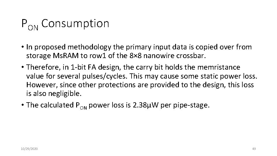
Proposed Sneak-path protection methodology üDesign can be faster without sneak-path current protection. üMemristor C 0 will contribute to the static power PON, insignificant amount. 8 -bit iterative adder design, PON = 2. 38µW with 40 nm halfpitch nanowire crossbar with VSET = 1. 0 V and PON = 0. 38µW with 8 nm half-pitch nanowire crossbar with VSET = 0. 4 V. üEither one row or one column connects to ground at a time, there can be only one path from VSET to Gnd at a time. üMemristors are turned down to the “reset” state through the VCLEAR signal in each row after operation completes. 10/29/2020 23

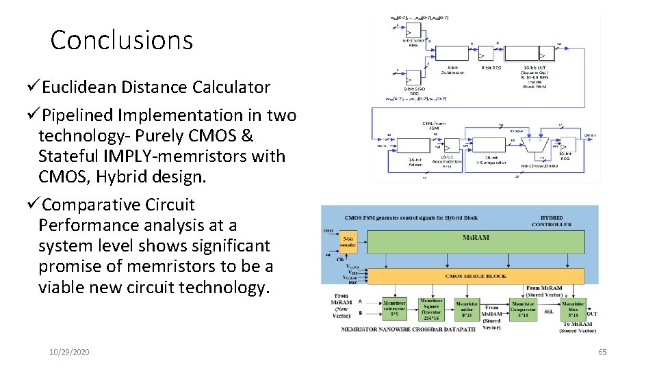
Proposed CMOS Pipelined Implementation of Euclidean Distance Calculator • four pipe-stages 10/29/2020 24

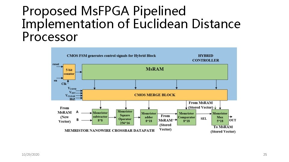
Proposed Ms. FPGA Pipelined Implementation of Euclidean Distance Processor 10/29/2020 25

CMOS FPGA Design for ED Pipeline • Each element of the vector represents a pixel of an image with gray scale value between 0 -255 (i. e. 2^8). • Designed for 8 -bit wide vector, so arithmetic computations are based on 8 -bit. • Design coded using VHDL. • Simulated for functionality evaluation and synthesized for performance measurement using Xilinx® XA Vivado-2015. 2 tool with Kintex®-7 family based smallest chip xc 7 k 70 tfbg 484 -3 - total package size of 23 x 23 mm 2 - high-performance/low-power (HPL) 28 nm high-k metal gate (HKMG) process technology - optimized for best price-performance with a 2 X improvement compared to the previous Xilinx FPGA generations 10/29/2020 26

CMOS FPGA Design • CMOS FPGA design was driven by a 134 MHz clock frequency • Subtractor used is different from the normal adder-subtractor, which always produces a positive result. 10/29/2020 27

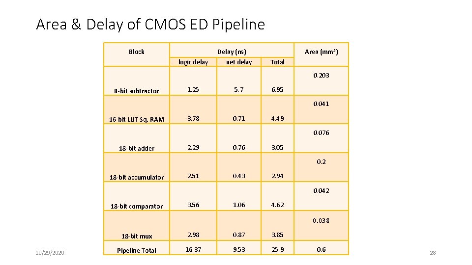
Area & Delay of CMOS ED Pipeline Block logic delay Delay (ns) net delay Area (mm 2) Total 0. 203 8 -bit subtractor 1. 25 5. 7 6. 95 0. 041 16 -bit LUT Sq. RAM 3. 78 0. 71 4. 49 0. 076 18 -bit adder 2. 29 0. 76 3. 05 0. 2 18 -bit accumulator 2. 51 0. 43 2. 94 0. 042 18 -bit comparator 3. 56 1. 06 4. 62 0. 038 10/29/2020 18 -bit mux 2. 98 0. 87 3. 85 Pipeline Total 16. 37 9. 53 25. 9 0. 6 28

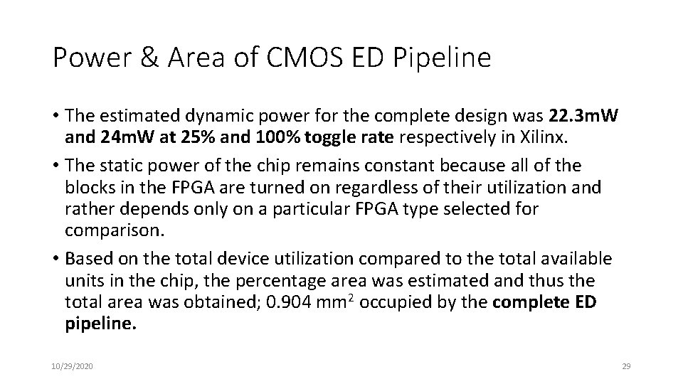
Power & Area of CMOS ED Pipeline • The estimated dynamic power for the complete design was 22. 3 m. W and 24 m. W at 25% and 100% toggle rate respectively in Xilinx. • The static power of the chip remains constant because all of the blocks in the FPGA are turned on regardless of their utilization and rather depends only on a particular FPGA type selected for comparison. • Based on the total device utilization compared to the total available units in the chip, the percentage area was estimated and thus the total area was obtained; 0. 904 mm 2 occupied by the complete ED pipeline. 10/29/2020 29

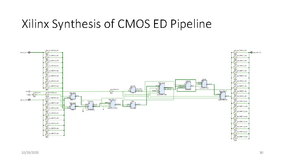
Xilinx Synthesis of CMOS ED Pipeline 10/29/2020 30

Performance Study of Proposed Ms. FPGA üMemristor Device Level PSPICE Simulation üMemristor Crossbar Nanowire PSPICE Simulations üArea Estimations üDelay Measurement üPower Calculations 10/29/2020 31

Memristor Device Level PSPICE Simulation: üThe memristor model used for SPICE simulation in this dissertation work is similar to that of the Biolek model. üBiolek model is a behavioral memristor model. üThe physical model was two-layer Ti. O 2 based, sandwiched between electrodes. One of the layers is doped with oxygen vacancies and thus it behaves as a semiconductor. The second layer, un-doped region, has an insulating property. üThe memristor circuit model here was implemented by using the software Or. CAD PSPICE. 10/29/2020 32

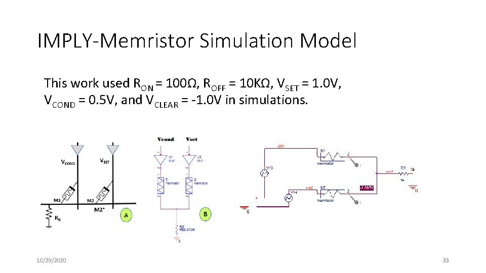
IMPLY-Memristor Simulation Model This work used RON = 100Ω, ROFF = 10 KΩ, VSET = 1. 0 V, VCOND = 0. 5 V, and VCLEAR = -1. 0 V in simulations. 10/29/2020 33

I-V Plot resembles the I-V plot obtained from simulation of Biolek model. 10/29/2020 34

IMPLY-Memristor Logic Evaluation Ti. O 2 Based Memristor Device Transition Delay Logical Combinations of M 1 M 2: 00, 01, 10 c u r r e n t 10/29/2020 Time 993. 21 ps 35

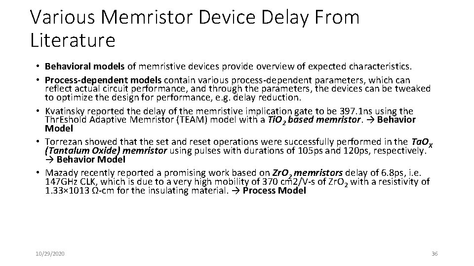
Various Memristor Device Delay From Literature • Behavioral models of memristive devices provide overview of expected characteristics. • Process-dependent models contain various process-dependent parameters, which can reflect actual circuit performance, and through the parameters, the devices can be tweaked to optimize the design for performance, e. g. delay reduction. • Kvatinsky reported the delay of the memristive implication gate to be 397. 1 ns using the Thr. Eshold Adaptive Memristor (TEAM) model with a Ti. O 2 based memristor. → Behavior Model • Torrezan showed that the set and reset operations were successfully performed in the Ta. OX (Tantalum Oxide) memristor using pulses with durations of 105 ps and 120 ps, respectively. → Behavior Model • Mazady recently reported a promising work based on Zr. O 2 memristors delay of 6. 8 ps, i. e. 147 GHz CLK, which is due to a very high mobility of 370 cm 2/V-s of Zr. O 2 with a resistivity of 1. 33× 1013 Ω-cm for the insulating material. → Process Model 10/29/2020 36

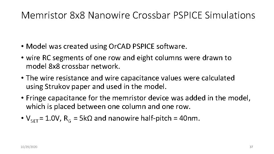
Memristor 8 x 8 Nanowire Crossbar PSPICE Simulations • Model was created using Or. CAD PSPICE software. • wire RC segments of one row and eight columns were drawn to model 8 x 8 crossbar network. • The wire resistance and wire capacitance values were calculated using Strukov paper and used in the model. • Fringe capacitance for the memristor device was added in the model, which is placed between one column and one row. • VSET = 1. 0 V, RG = 5 kΩ and nanowire half-pitch = 40 nm. 10/29/2020 37

RC Delay Measurement of the 8 x 8 Nanowire Crossbar Model Through PSPICE Simulations Simulation results showed negligible wire delay even for the worst case/farthest column from load resistor R G, the RC delay was only ~0. 075 fs. 10/29/2020 38

Before Performance Evaluation of Ms. FPGA • Before we can estimate the design area and delay, every memristorbased block in the Ms. FPGA system is designed with IMPLYmemristors using the space-time notation. Thus we know how many memristors or 8 x 8 crossbar block(s) and how many pulses are required for designing each component or block. • The number of memristors is used for the layout area estimation and the number of pulses is used for the delay calculation. 10/29/2020 39

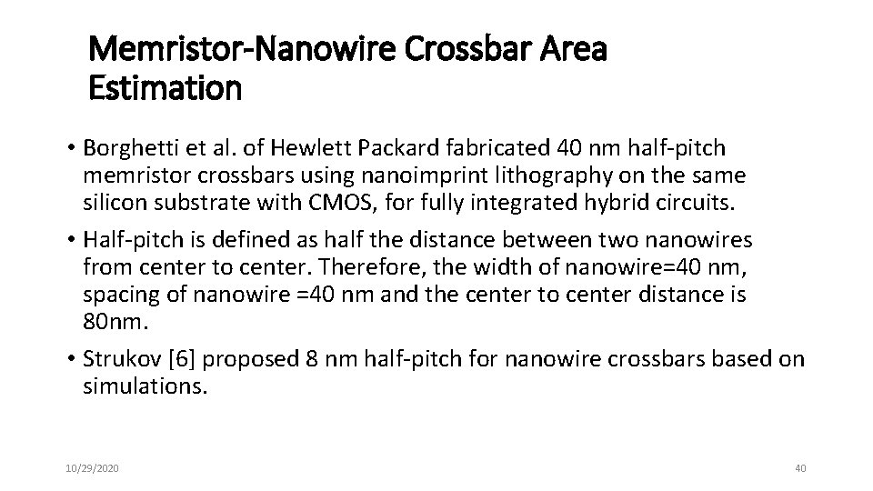
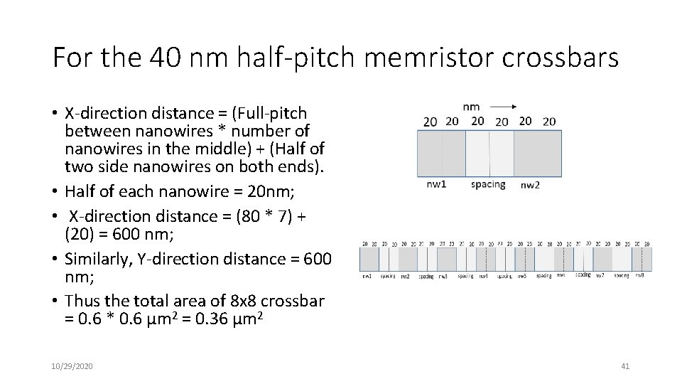
Memristor-Nanowire Crossbar Area Estimation • Borghetti et al. of Hewlett Packard fabricated 40 nm half-pitch memristor crossbars using nanoimprint lithography on the same silicon substrate with CMOS, for fully integrated hybrid circuits. • Half-pitch is defined as half the distance between two nanowires from center to center. Therefore, the width of nanowire=40 nm, spacing of nanowire =40 nm and the center to center distance is 80 nm. • Strukov [6] proposed 8 nm half-pitch for nanowire crossbars based on simulations. 10/29/2020 40

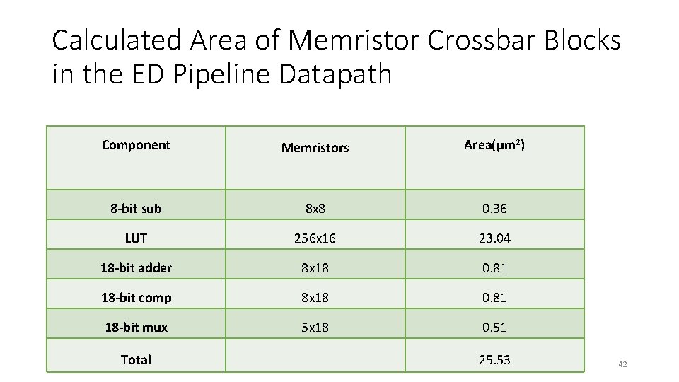
For the 40 nm half-pitch memristor crossbars • X-direction distance = (Full-pitch between nanowires * number of nanowires in the middle) + (Half of two side nanowires on both ends). • Half of each nanowire = 20 nm; • X-direction distance = (80 * 7) + (20) = 600 nm; • Similarly, Y-direction distance = 600 nm; • Thus the total area of 8 x 8 crossbar = 0. 6 * 0. 6 µm 2 = 0. 36 µm 2 10/29/2020 41

Calculated Area of Memristor Crossbar Blocks in the ED Pipeline Datapath Component Memristors 10/29/2020 Area(µm 2) 8 -bit sub 8 x 8 0. 36 LUT 256 x 16 23. 04 18 -bit adder 8 x 18 0. 81 18 -bit comp 8 x 18 0. 81 18 -bit mux 5 x 18 0. 51 Total 25. 53 42

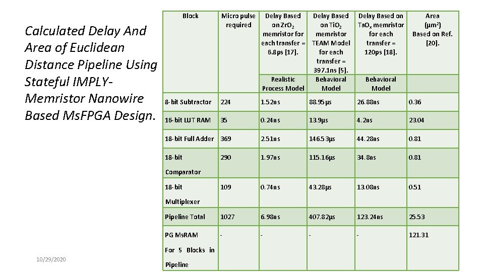
Datapath, Ms. RAM and Total Area of ED Pipeline • Since the total number of micro-pulses for the complete pipeline is 1027 and the total number of control bits is 21, therefore the total Ms. RAM area was calculated: • Ms. RAM area = ((Total number of micro-pulses * Total number of control bits) * Total area for 8 x 8 crossbar)/Total number of memristors in an 8 x 8 crossbar. • Thus, the total Ms. RAM area for the ED pipeline is calculated as 121. 31µm 2. • Based on 40 nm half-pitch, the estimated area of the proposed ED pipeline datapath is 25. 5µm 2, with corresponding Ms. RAM area in Pulse Generator is 121µm 2. Therefore, the total area consumed by the complete ED pipeline is 146µm 2. • Based on Strukov’s 8 nm half-pitch nanowires, the total area requirement of the same ED pipeline is only 5. 9µm 2. 10/29/2020 43

Block Calculated Delay And Area of Euclidean Distance Pipeline Using Stateful IMPLYMemristor Nanowire Based Ms. FPGA Design. Micro pulse Delay Based on Area required on Zr. O 2 on Ti. O 2 Ta. Ox memristor (µm 2) memristor for each Based on Ref. each transfer = TEAM Model transfer = [20]. 6. 8 ps [17]. for each 120 ps [18]. transfer = 397. 1 ns [5]. Realistic Behavioral Process Model 8 -bit Subtractor 224 1. 52 ns 88. 95µs 26. 88 ns 0. 36 16 -bit LUT RAM 35 0. 24 ns 13. 9µs 4. 2 ns 23. 04 18 -bit Full Adder 369 2. 51 ns 146. 53µs 44. 28 ns 0. 81 18 -bit 290 1. 97 ns 115. 16µs 34. 8 ns 0. 81 109 0. 74 ns 43. 28µs 13. 08 ns 0. 51 Pipeline Total 1027 6. 98 ns 407. 82µs 123. 24 ns 25. 53 PG Ms. RAM - - 121. 31 Comparator 18 -bit Multiplexer For 5 Blocks in 10/29/2020 Pipeline 44
![Power Consumption Sources of MemristorNanowire Design Strukov 10292020 45 Power Consumption Sources of Memristor-Nanowire Design [Strukov] • 10/29/2020 45](https://slidetodoc.com/presentation_image/1d74422753b663503afbd4c8a62e83db/image-45.jpg)
Power Consumption Sources of Memristor-Nanowire Design [Strukov] • 10/29/2020 45

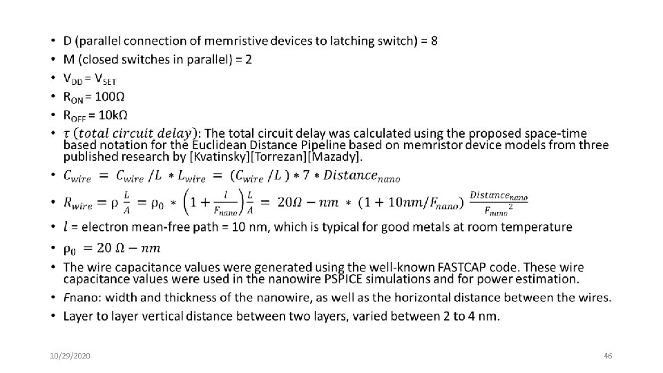
• 10/29/2020 46

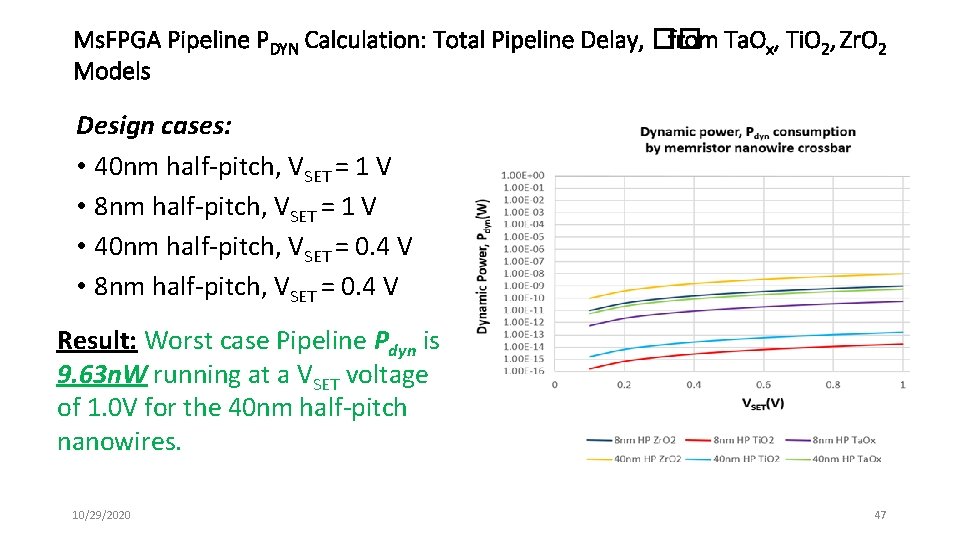
Ms. FPGA Pipeline PDYN Calculation: Total Pipeline Delay, �� from Ta. Ox, Ti. O 2, Zr. O 2 Models Design cases: • 40 nm half-pitch, VSET = 1 V • 8 nm half-pitch, VSET = 1 V • 40 nm half-pitch, VSET = 0. 4 V • 8 nm half-pitch, VSET = 0. 4 V Result: Worst case Pipeline Pdyn is 9. 63 n. W running at a VSET voltage of 1. 0 V for the 40 nm half-pitch nanowires. 10/29/2020 47

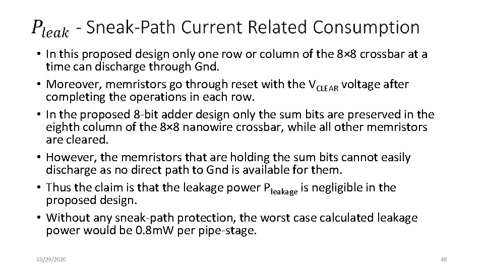
• In this proposed design only one row or column of the 8× 8 crossbar at a time can discharge through Gnd. • Moreover, memristors go through reset with the VCLEAR voltage after completing the operations in each row. • In the proposed 8 -bit adder design only the sum bits are preserved in the eighth column of the 8× 8 nanowire crossbar, while all other memristors are cleared. • However, the memristors that are holding the sum bits cannot easily discharge as no direct path to Gnd is available for them. • Thus the claim is that the leakage power Pleakage is negligible in the proposed design. • Without any sneak-path protection, the worst case calculated leakage power would be 0. 8 m. W per pipe-stage. 10/29/2020 48

PON Consumption • In proposed methodology the primary input data is copied over from storage Ms. RAM to row 1 of the 8× 8 nanowire crossbar. • Therefore, in 1 -bit FA design, the carry bit holds the memristance value for several pulses/cycles. This may cause some static power loss. However, since other protections are provided to the design, this loss is also negligible. • The calculated PON power loss is 2. 38µW per pipe-stage. 10/29/2020 49

CMOS Power Component of Ms. FPGA • The estimated total dynamic power consumption by CMOS circuitry per 8× 8 memristive nanowire crossbar (per pipe-stage) is 2. 25 m. W at 25% toggle rate • Thus, for four pipe-stages of the complete ED pipeline, it is approximately 9 m. W. • Proposed hybrid Ms. FPGA operating at 1. 0 V consumes ~9 m. W total dynamic power as the power components from memristor design is insignificant. 10/29/2020 50

CMOS Area of Ms. FPGA üCMOS circuitry in the hybrid Ms. FPGA consumes 0. 32 mm 2 area as estimated. üThe area of the hybrid Ms. FPGA design is dominated by the CMOS components. üNanowire is fabricated on top of CMOS. üAs the memristor crossbar technology matures, more components can be converted from CMOS to memristors and thus these components can be moved to the memristor layer from the CMOS layer. 10/29/2020 51

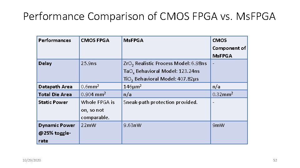
Performance Comparison of CMOS FPGA vs. Ms. FPGA Performances CMOS FPGA Ms. FPGA Delay 25. 9 ns Zr. O 2 Realistic Process Model: 6. 98 ns Ta. Ox Behavioral Model: 123. 24 ns Ti. O 2 Behavioral Model: 407. 82µs 146µm 2 n/a Sneak-path protection provided. Datapath Area Total Die Area Static Power 0. 6 mm 2 0. 904 mm 2 Whole FPGA is on, so not comparable. Dynamic Power 22 m. W @25% togglerate 10/29/2020 9. 63 n. W CMOS Component of Ms. FPGA - n/a 0. 32 mm 2 - 9 m. W 52

Contributions: Circuit Methodology • Presented optimized design for logic blocks using IMPLY-memristor. • An innovative concept of an 8 -bit iterative adder design using the Stateful IMPLY-memristor is presented. • The 8 -bit iterative adder is designed in a new type of 8 x 8 nanowire crossbar, where, each adder bit is implemented in one row of the 8 -row crossbar network. • The design is optimized for area, power and delay and has sneak-path protection for logical error. • Similarly, components of 8 -bit, 16 -bit, or any other order bit can be designed using one or multiple 8 x 8 crossbar blocks, as needed. • For this dissertation other arithmetic blocks, e. g. subtractor, comparator, multiplexer, square-operator blocks were also designed using the same design concepts. 10/29/2020 53

Contributions: Circuit Methodology Array of 8 x 8 Nanowire Crossbar Block • The innovative pipelining concept is presented for the datapath design using an array of 8 x 8 nanowire crossbar blocks. • This array of blocks can grow both horizontally as well as vertically and can act as a pipeline in either way. • Therefore, multiple arithmetic operations can simultaneously execute. • Improves overall design speed that can compensate for slowness in memristors devices. 10/29/2020 54

Contributions: Circuit Methodology • Novel ideas that are valuable to the development of memristor technology. • Proposed Ms. CMOL: Conventional CMOL cannot be conveniently used for logic design using memristors. Proposed novel Ms. CMOL can be used for Logic, Memory and Connections. • Idea of data storage Ms. RAM: Receives the image feature vectors in the data storage Ms. RAM, which later copies the data over to the Datapath. • Array of 8 x 8 nanowire crossbar blocks: Enables pipelining and parallelism, which helps speed-up the memristor based design. • Proposed row-to-row data transfer: Voltages are applied through columns to execute operations. Once data is ready in the current row and needs to move to the next row, voltages are applied through rows to copy data from current row to the next row. 10/29/2020 55

Contributions: Circuit Methodology • Proposed sneak-path protection: Major concern of all crossbar nanowire design for logical error and power loss. • Proposed design was presented with an example 8 -bit Full iterative adder design. • This design is free of dangerous logical errors and it was minimized for possible power consumption. • The power consumption for this proposed design is reduced to the lowest possible level. • This proposed sneak-path free combinatorial circuit design methodology is much more robust and simple than any other published research on similar designs with nanowire crossbars. 10/29/2020 56

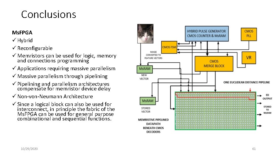
Contributions: Architecture Methodology • Dissertation presented Innovative concepts for the memristive FPGA design. • Ms. FPGA (Memristive stateful logic Field Programmable Gate Array): A novel Memristor -CMOS Hybrid Reconfigurable Architecture was proposed. • Ms. FPGA uses memristors for memory, connections programming, and combinational logic implementation as opposed to other published memristor based FPGAs, for example mr. FPGA, where memristors are reconfigured for logic connections only. • Proposes a Non-von-Neumann architecture where DP and memory does not need to be separated. • Ms. FPGA is intended for highly parallel regular architectures in which blocks are placed in abutment and in which horizontal connections are short. • Pipelining and Parallelism: The proposed Ms. FPGA is a reconfigurable system that can be designed with pipelined datapaths and massive parallelism in the datapath. • The pipelining is designed by simultaneously executing multiple operations using several 8 x 8 crossbar blocks. • The parallelism can be designed by simultaneously driving many such pipelines with one controller, using the SIMD (Single Instruction Multiple Data) concept. 10/29/2020 57

Contributions: Architecture Methodology • Proposes a novel general new architecture model, Memristive stateful Finite State Machine with Datapath (Ms. FSMD). Like conventional FSMD, this proposed system is also a digital system that includes a finite-state machine, and a datapath, but all logic is implemented with memristors, which changes timing and design methods used. • Ms. FSMD model has an additional control block called the pulse generator. The pulse generator can be defined as the brain of the proposed Ms. FPGA. • The pulse generation block contains the Memristive stateful Random Access Memory (Ms. RAM). This Ms. RAM, another innovation of this dissertation work, contains all the configuration information required to realize the virtual logic circuit in the memristive nanowire crossbar datapath. The Ms. RAM is a memory while the datapath is a fabric. 10/29/2020 58

Contributions: Hardware Realization of Euclidean Distance Calculator • Proposed the hardware implementation of the Euclidean Distance Calculator as an innovative pipelined datapath. • Presented this datapath as a CMOS FPGA design as well as a memristive FPGA design with performance analysis. • Euclidean Distance calculation used in many neural network and associative memory based software algorithms, the hardware realization of the Euclidean Distance Calculator as a pipelined datapath with memristors is an important concept. 10/29/2020 59

Contributions: Design Execution Methodology • Presented the detailed area, power and delay measurement and calculation methods -for CMOS FPGA and proposed Ms. FPGA. • Performed the performance comparisons of CMOS FPGA versus Proposed Ms. FPGA designs using the example, Euclidean Distance pipelined datapath. • A new contribution as no other published research presented such performance comparisons between the two technologies for complete systems with simulated results. 10/29/2020 60

Conclusions Ms. FPGA ü Hybrid ü Reconfigurable ü Memristors can be used for logic, memory and connections programming ü Applications requiring massive parallelism ü Massive parallelism through pipelining ü Pipelining and parallelism architectures compensate for memristor device delay ü Non-von-Neumann Architecture ü Since a logical block can also be used for interconnect, in principle the fabric of the Ms. FPGA can be used for general purpose combinational and sequential functions. 10/29/2020 61

Conclusions üMs. FPGA is particularly suited to regular designs with rectangular or square blocks (8 x 8 nanowire crossbar blocks) executed in parallel or pipelined. üSince the blocks communicate mostly by abutting, the routing is simplified. This makes architecture specifically suitable for regular SIMD, systolic and pipelined architectures, which are typical to DSP, neural network and image processing. üDatapath is a fabric. 10/29/2020 62

Conclusions üMs. FSMD: Hybrid controller & a new type of DP-memory üMs. RAM in Pulse Generator üMs. CMOL 10/29/2020 63

Conclusions üProvides Sneak-path protection - eliminates dangerous logical error - power loss 10/29/2020 64

Conclusions üEuclidean Distance Calculator üPipelined Implementation in two technology- Purely CMOS & Stateful IMPLY-memristors with CMOS, Hybrid design. üComparative Circuit Performance analysis at a system level shows significant promise of memristors to be a viable new circuit technology. 10/29/2020 65

Publications: • Journal Publication (conditionally accepted): Rahman, K. C. , Hammerstrom, D. , Li, Y. , Xiong, H. , & Perkowski, M. "Methodology and Design of a Massively Parallel Memristive Stateful IMPLY Logic based Reconfigurable Architecture. " Nanotechnology, IEEE Transactions on (2016): xx. • Patent: Rahman, K. C. , Perkowski, M. , Hammerstrom, D. , & Al-Jafar M. filed Provisional Patent Application No. 61/989, 387. 10/29/2020 66

Questions? 10/29/2020 67

Additional Slides: 10/29/2020 68

Conventional CMOL 10/29/2020 69

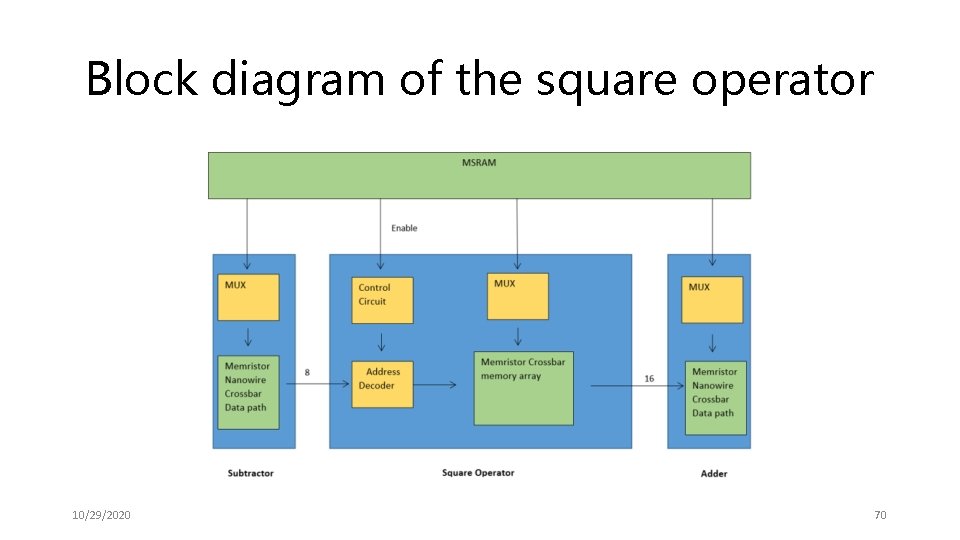
Block diagram of the square operator 10/29/2020 70

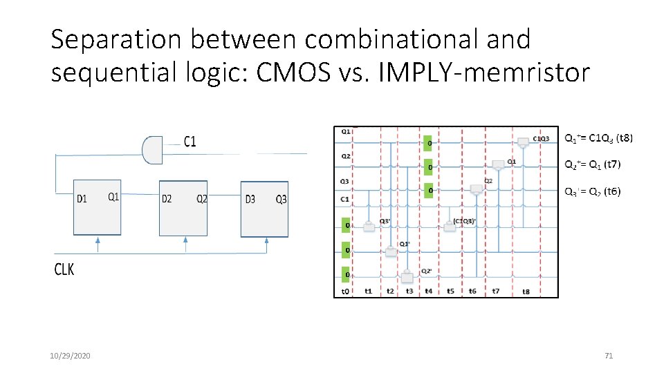
Separation between combinational and sequential logic: CMOS vs. IMPLY-memristor 10/29/2020 71