Compact modeling of advanced bulk CMOS using EKV
Compact modeling of advanced bulk CMOS using EKV 3 – linearity, RF and noise performance trends Matthias Bucher, Angelos Antonopoulos Technical University of Crete bucher@electronics. tuc. gr
Outline • Physics-based, charge-based compact MOSFET model – EKV 3 model • DC to RF modeling • IV, CV, Y-parameters • Linearity • RF figures of merit – evolution with technology • Thermal noise • Conclusions WMF: Physics-Based NL CM for mm-Wave Applications IMS 2014, Tampa, 1 -6 June, 2014 2

EKV 3 scalable model for high frequency • Scalability vs. channel length, number of fingers, bias – Gate- and substrate- parasitics scale with multi-finger layout – Layout-dependent stress effects • Non quasi-static model (NQS) – channel segmentation – consistent AC/transient • Thermal noise – Induced gate & substrate noise – Velocity saturation, CLM – Carrier heating WMF: Physics-Based NL CM for mm-Wave Applications IMS 2014, Tampa, 1 -6 June, 2014 3
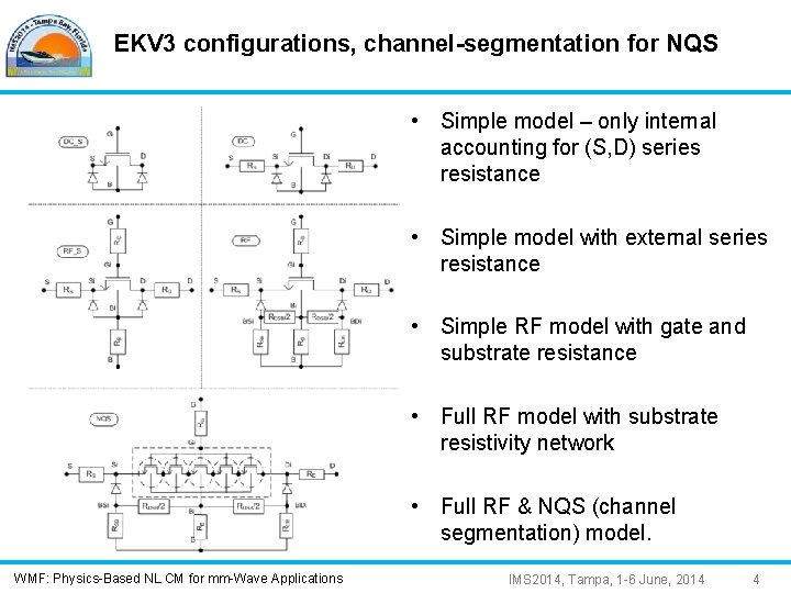
EKV 3 configurations, channel-segmentation for NQS • Simple model – only internal accounting for (S, D) series resistance • Simple model with external series resistance • Simple RF model with gate and substrate resistance • Full RF model with substrate resistivity network • Full RF & NQS (channel segmentation) model. WMF: Physics-Based NL CM for mm-Wave Applications IMS 2014, Tampa, 1 -6 June, 2014 4
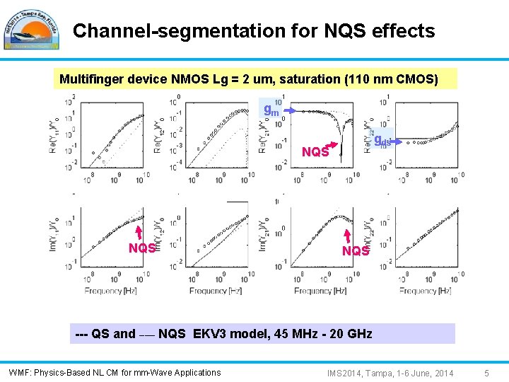
Channel-segmentation for NQS effects Multifinger device NMOS Lg = 2 um, saturation (110 nm CMOS) gm gds NQS NQS --- QS and ___ NQS EKV 3 model, 45 MHz - 20 GHz WMF: Physics-Based NL CM for mm-Wave Applications IMS 2014, Tampa, 1 -6 June, 2014 5
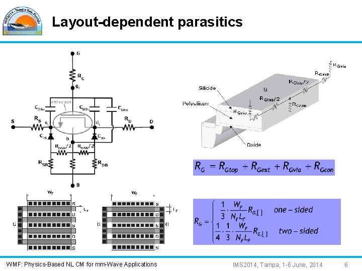
Layout-dependent parasitics WMF: Physics-Based NL CM for mm-Wave Applications IMS 2014, Tampa, 1 -6 June, 2014 6
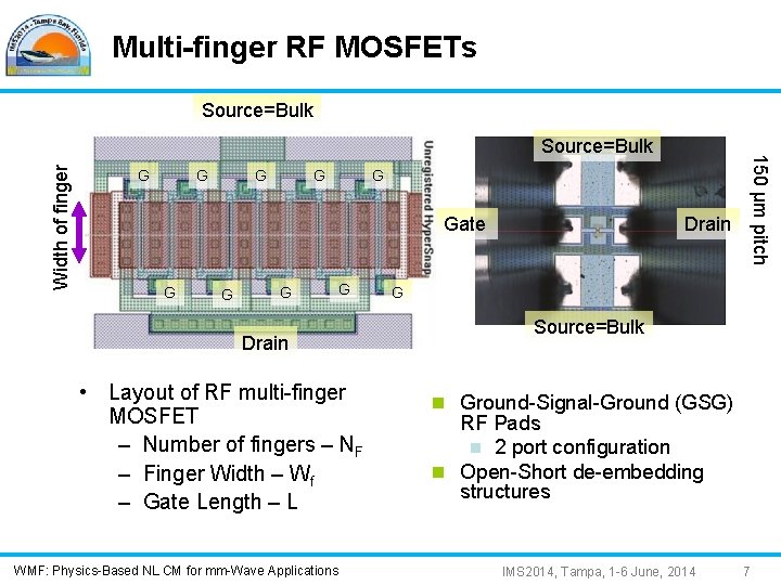
Multi-finger RF MOSFETs Source=Bulk Width of finger G G Gate G G Drain • Layout of RF multi-finger MOSFET – Number of fingers – NF – Finger Width – Wf – Gate Length – L WMF: Physics-Based NL CM for mm-Wave Applications Drain 150 μm pitch Source=Bulk G Source=Bulk n Ground-Signal-Ground (GSG) RF Pads n 2 port configuration n Open-Short de-embedding structures IMS 2014, Tampa, 1 -6 June, 2014 7
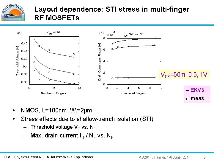
Layout dependence: STI stress in multi-finger RF MOSFETs VDS=50 m, 0. 5, 1 V – EKV 3 □ meas. • NMOS, L=180 nm, Wf=2μm • Stress effects due to shallow-trench isolation (STI) – Threshold voltage VT vs. NF – Max. drain current ID / NF vs. NF WMF: Physics-Based NL CM for mm-Wave Applications IMS 2014, Tampa, 1 -6 June, 2014 8
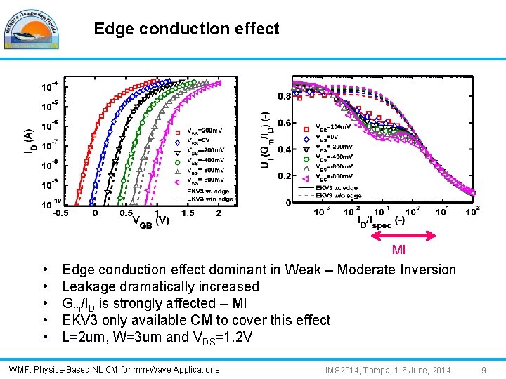
Edge conduction effect MI • • • Edge conduction effect dominant in Weak – Moderate Inversion Leakage dramatically increased Gm/ID is strongly affected – MI EKV 3 only available CM to cover this effect L=2 um, W=3 um and VDS=1. 2 V WMF: Physics-Based NL CM for mm-Wave Applications IMS 2014, Tampa, 1 -6 June, 2014 9
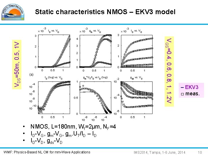
Static characteristics NMOS – EKV 3 model VDS=50 m, 0. 5, 1 V VGS=0. 4, 0. 6, 0. 8, 1, 1. 2 V – EKV 3 □ meas. • NMOS, L=180 nm, Wf=2μm, NF=4 • ID-VG, gm. UT/ID – ID • ID-VD, gds-VD WMF: Physics-Based NL CM for mm-Wave Applications IMS 2014, Tampa, 1 -6 June, 2014 10
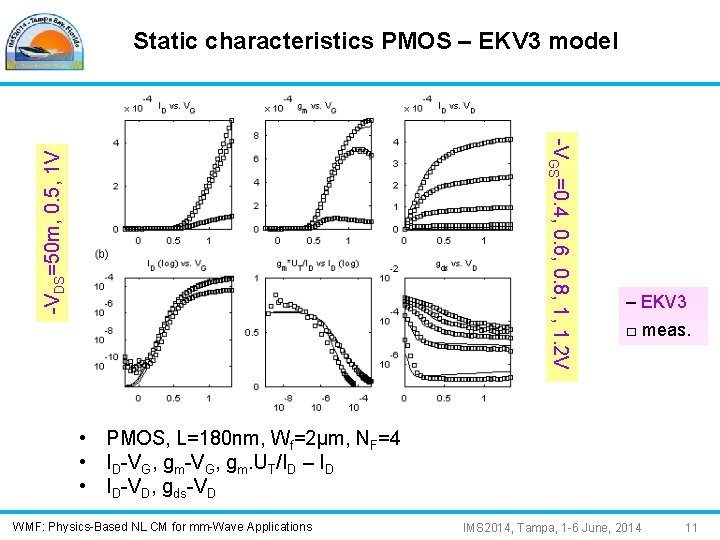
Static characteristics PMOS – EKV 3 model -VDS=50 m, 0. 5, 1 V -VGS=0. 4, 0. 6, 0. 8, 1, 1. 2 V – EKV 3 □ meas. • PMOS, L=180 nm, Wf=2μm, NF=4 • ID-VG, gm. UT/ID – ID • ID-VD, gds-VD WMF: Physics-Based NL CM for mm-Wave Applications IMS 2014, Tampa, 1 -6 June, 2014 11
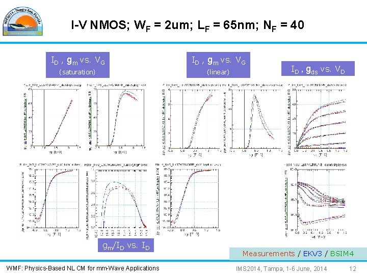
I-V NMOS; WF = 2 um; LF = 65 nm; NF = 40 ID , gm vs. VG (saturation) (linear) gm/ID vs. ID WMF: Physics-Based NL CM for mm-Wave Applications ID , gds vs. VD Measurements / EKV 3 / BSIM 4 IMS 2014, Tampa, 1 -6 June, 2014 12
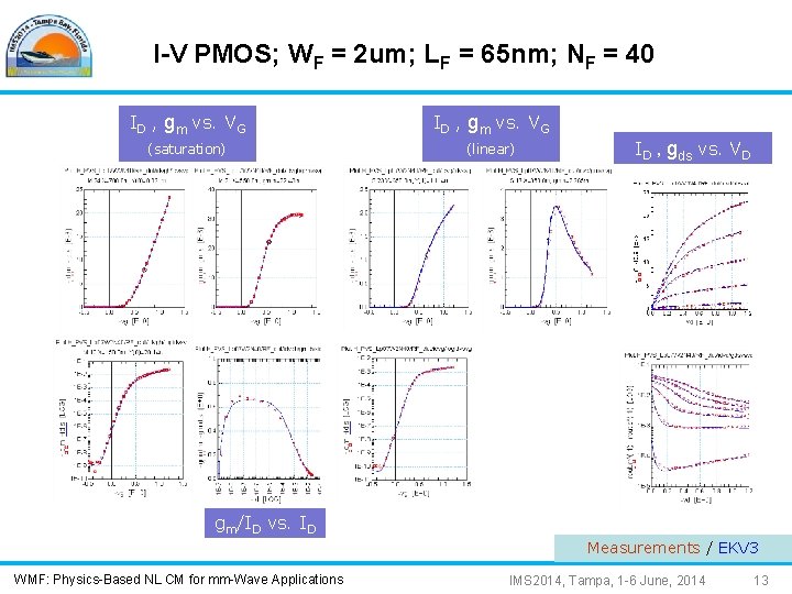
I-V PMOS; WF = 2 um; LF = 65 nm; NF = 40 ID , gm vs. VG (saturation) (linear) ID , gds vs. VD gm/ID vs. ID Measurements / EKV 3 WMF: Physics-Based NL CM for mm-Wave Applications IMS 2014, Tampa, 1 -6 June, 2014 13
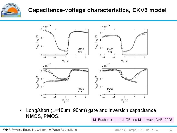
Capacitance-voltage characteristics, EKV 3 model • Long/short (L=10 um, 90 nm) gate and inversion capacitance, NMOS, PMOS. M. Bucher e. a. Int. J. RF and Microwave CAE, 2008 WMF: Physics-Based NL CM for mm-Wave Applications IMS 2014, Tampa, 1 -6 June, 2014 14
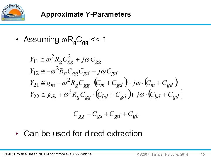
Approximate Y-Parameters • Assuming w. Rg. Cgg << 1 • Can be used for direct extraction WMF: Physics-Based NL CM for mm-Wave Applications IMS 2014, Tampa, 1 -6 June, 2014 15
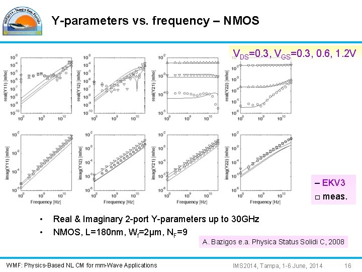
Y-parameters vs. frequency – NMOS VDS=0. 3, VGS=0. 3, 0. 6, 1. 2 V – EKV 3 □ meas. • • Real & Imaginary 2 -port Y-parameters up to 30 GHz NMOS, L=180 nm, Wf=2μm, NF=9 A. Bazigos e. a. Physica Status Solidi C, 2008 WMF: Physics-Based NL CM for mm-Wave Applications IMS 2014, Tampa, 1 -6 June, 2014 16
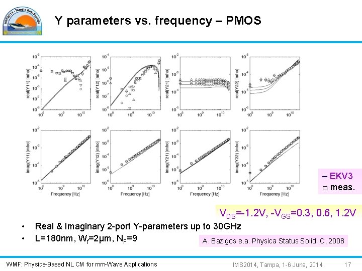
Y parameters vs. frequency – PMOS – EKV 3 □ meas. VDS=-1. 2 V, -VGS=0. 3, 0. 6, 1. 2 V • • Real & Imaginary 2 -port Y-parameters up to 30 GHz L=180 nm, Wf=2μm, NF=9 A. Bazigos e. a. Physica Status Solidi C, 2008 WMF: Physics-Based NL CM for mm-Wave Applications IMS 2014, Tampa, 1 -6 June, 2014 17
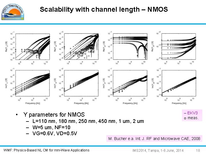
Scalability with channel length – NMOS • Y parameters for NMOS – L=110 nm, 180 nm, 250 nm, 450 nm, 1 um, 2 um – W=5 um, NF=10 – VG=0. 6 V, VD=0. 5 V – EKV 3 □ meas. M. Bucher e. a. Int. J. RF and Microwave CAE, 2008 WMF: Physics-Based NL CM for mm-Wave Applications IMS 2014, Tampa, 1 -6 June, 2014 18
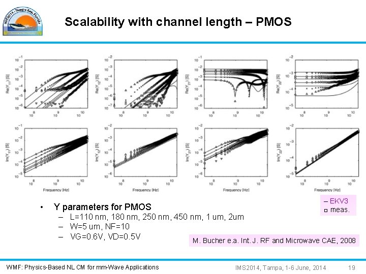
Scalability with channel length – PMOS • Y parameters for PMOS – EKV 3 □ meas. – L=110 nm, 180 nm, 250 nm, 450 nm, 1 um, 2 um – W=5 um, NF=10 – VG=0. 6 V, VD=0. 5 V M. Bucher e. a. Int. J. RF and Microwave CAE, 2008 WMF: Physics-Based NL CM for mm-Wave Applications IMS 2014, Tampa, 1 -6 June, 2014 19
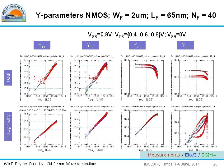
Y-parameters NMOS; WF = 2 um; LF = 65 nm; NF = 40 VGS=0. 8 V; VDS={0. 4, 0. 6, 0. 8}V; VSB=0 V Y 12 Y 21 Y 22 imaginary real Y 11 Measurements / EKV 3 / BSIM 4 WMF: Physics-Based NL CM for mm-Wave Applications IMS 2014, Tampa, 1 -6 June, 2014 20
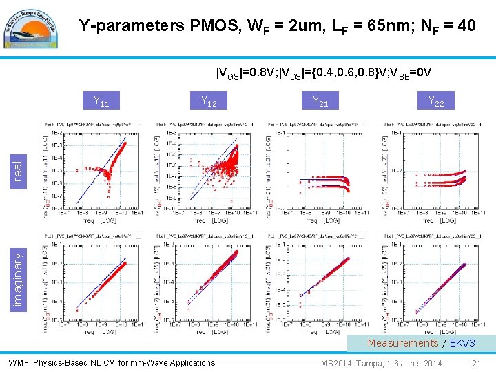
Y-parameters PMOS, WF = 2 um, LF = 65 nm; NF = 40 |VGS|=0. 8 V; |VDS|={0. 4, 0. 6, 0. 8}V; VSB=0 V Y 12 Y 21 Y 22 imaginary real Y 11 Measurements / EKV 3 WMF: Physics-Based NL CM for mm-Wave Applications IMS 2014, Tampa, 1 -6 June, 2014 21
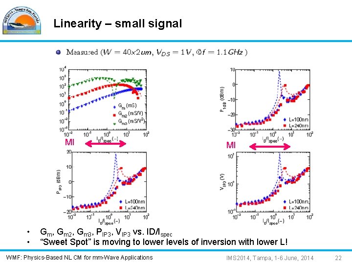
Linearity – small signal MI • • MI Gm, Gm 2, Gm 3, PIP 3, VIP 3 vs. ID/Ispec “Sweet Spot” is moving to lower levels of inversion with lower L! WMF: Physics-Based NL CM for mm-Wave Applications IMS 2014, Tampa, 1 -6 June, 2014 22
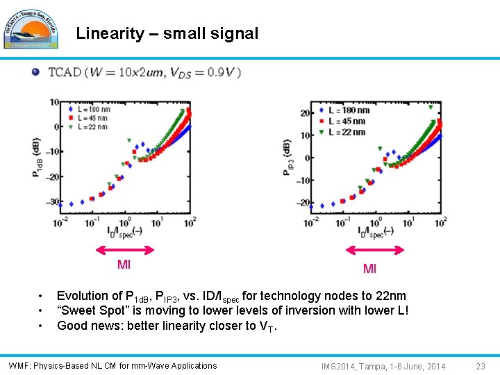
Linearity – small signal MI • • • MI Evolution of P 1 d. B, PIP 3, vs. ID/Ispec for technology nodes to 22 nm “Sweet Spot” is moving to lower levels of inversion with lower L! Good news: better linearity closer to VT. WMF: Physics-Based NL CM for mm-Wave Applications IMS 2014, Tampa, 1 -6 June, 2014 23
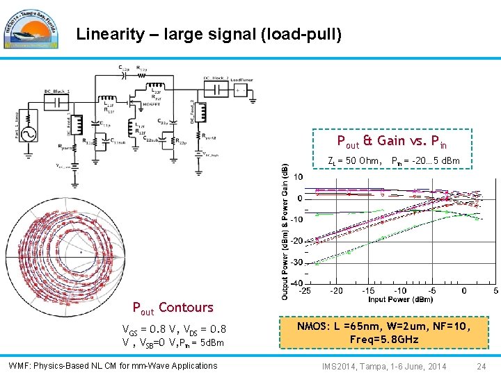
Linearity – large signal (load-pull) Pout & Gain vs. Pin ZL = 50 Ohm, Pin = -20… 5 d. Bm Pout Contours VGS = 0. 8 V, VDS = 0. 8 V , VSB=0 V, Pin = 5 d. Bm WMF: Physics-Based NL CM for mm-Wave Applications NMOS: L =65 nm, W=2 um, NF=10, Freq=5. 8 GHz IMS 2014, Tampa, 1 -6 June, 2014 24
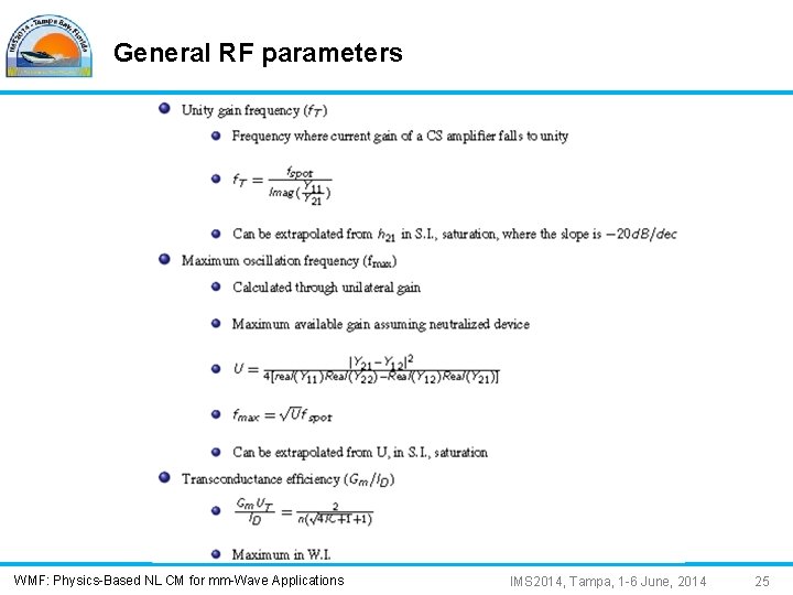
General RF parameters WMF: Physics-Based NL CM for mm-Wave Applications IMS 2014, Tampa, 1 -6 June, 2014 25
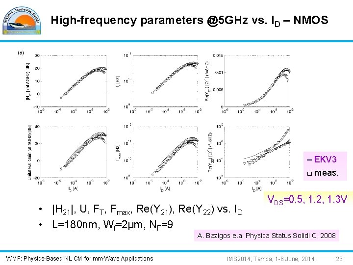
High-frequency parameters @5 GHz vs. ID – NMOS – EKV 3 □ meas. • |H 21|, U, FT, Fmax, Re(Y 21), Re(Y 22) vs. ID • L=180 nm, Wf=2μm, NF=9 VDS=0. 5, 1. 2, 1. 3 V A. Bazigos e. a. Physica Status Solidi C, 2008 WMF: Physics-Based NL CM for mm-Wave Applications IMS 2014, Tampa, 1 -6 June, 2014 26
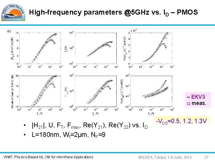
High-frequency parameters @5 GHz vs. ID – PMOS – EKV 3 □ meas. • |H 21|, U, FT, Fmax, Re(Y 21), Re(Y 22) vs. ID • L=180 nm, Wf=2μm, NF=9 WMF: Physics-Based NL CM for mm-Wave Applications -VDS=0. 5, 1. 2, 1. 3 V IMS 2014, Tampa, 1 -6 June, 2014 27
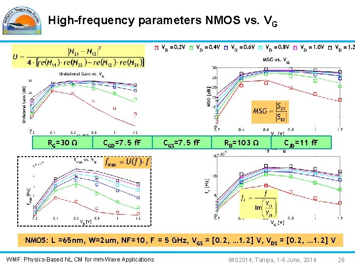
High-frequency parameters NMOS vs. VG RG=30 Ω CGD=7. 5 f. F CGS=7. 5 f. F RB=103 Ω CJD=11 f. F NMOS: L =65 nm, W=2 um, NF=10, F = 5 GHz, VGS = [0. 2, … 1. 2] V, VDS = [0. 2, … 1. 2] V WMF: Physics-Based NL CM for mm-Wave Applications IMS 2014, Tampa, 1 -6 June, 2014 28
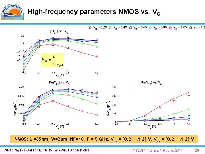
High-frequency parameters NMOS vs. VG NMOS: L =65 nm, W=2 um, NF=10, F = 5 GHz, VGS = [0. 2, … 1. 2] V, VDS = [0. 2, … 1. 2] V WMF: Physics-Based NL CM for mm-Wave Applications IMS 2014, Tampa, 1 -6 June, 2014 29
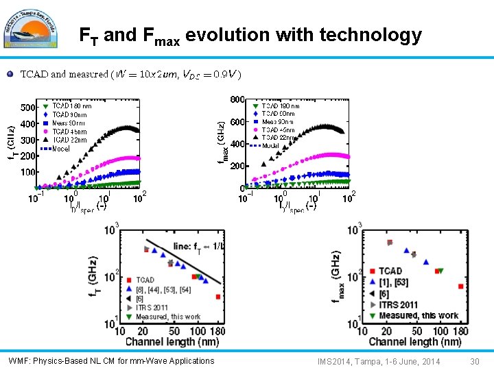
FT and Fmax evolution with technology WMF: Physics-Based NL CM for mm-Wave Applications IMS 2014, Tampa, 1 -6 June, 2014 30
![GM /ID·FT, GM 2/ID and [GM /GDS·GM /ID FT] The different Fo. Ms behave GM /ID·FT, GM 2/ID and [GM /GDS·GM /ID FT] The different Fo. Ms behave](http://slidetodoc.com/presentation_image_h2/8b228cfef22a53e5b473f09e32a8f9ad/image-31.jpg)
GM /ID·FT, GM 2/ID and [GM /GDS·GM /ID FT] The different Fo. Ms behave in a similar way Maximum in moderate inversion! Trend towards lower levels (within moderate inversion) WMF: Physics-Based NL CM for mm-Wave Applications IMS 2014, Tampa, 1 -6 June, 2014 31
![GM /ID·FT and [GM /GDS·GM /ID FT] evolution WMF: Physics-Based NL CM for mm-Wave GM /ID·FT and [GM /GDS·GM /ID FT] evolution WMF: Physics-Based NL CM for mm-Wave](http://slidetodoc.com/presentation_image_h2/8b228cfef22a53e5b473f09e32a8f9ad/image-32.jpg)
GM /ID·FT and [GM /GDS·GM /ID FT] evolution WMF: Physics-Based NL CM for mm-Wave Applications IMS 2014, Tampa, 1 -6 June, 2014 32
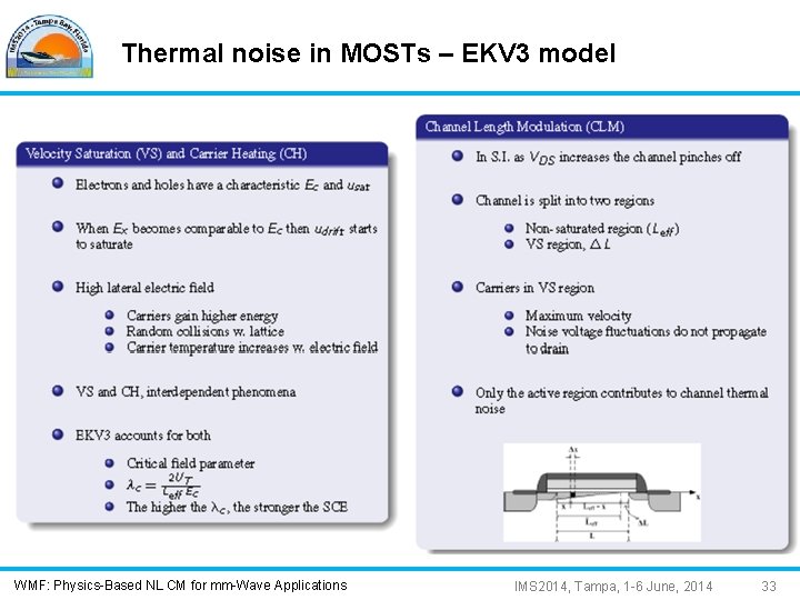
Thermal noise in MOSTs – EKV 3 model WMF: Physics-Based NL CM for mm-Wave Applications IMS 2014, Tampa, 1 -6 June, 2014 33
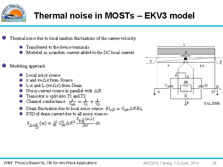
Thermal noise in MOSTs – EKV 3 model WMF: Physics-Based NL CM for mm-Wave Applications IMS 2014, Tampa, 1 -6 June, 2014 34
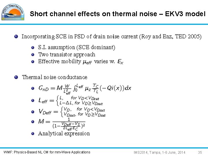
Short channel effects on thermal noise – EKV 3 model WMF: Physics-Based NL CM for mm-Wave Applications IMS 2014, Tampa, 1 -6 June, 2014 35
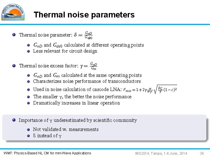
Thermal noise parameters WMF: Physics-Based NL CM for mm-Wave Applications IMS 2014, Tampa, 1 -6 June, 2014 36
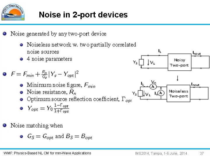
Noise in 2 -port devices WMF: Physics-Based NL CM for mm-Wave Applications IMS 2014, Tampa, 1 -6 June, 2014 37
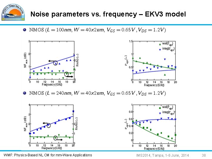
Noise parameters vs. frequency – EKV 3 model WMF: Physics-Based NL CM for mm-Wave Applications IMS 2014, Tampa, 1 -6 June, 2014 38
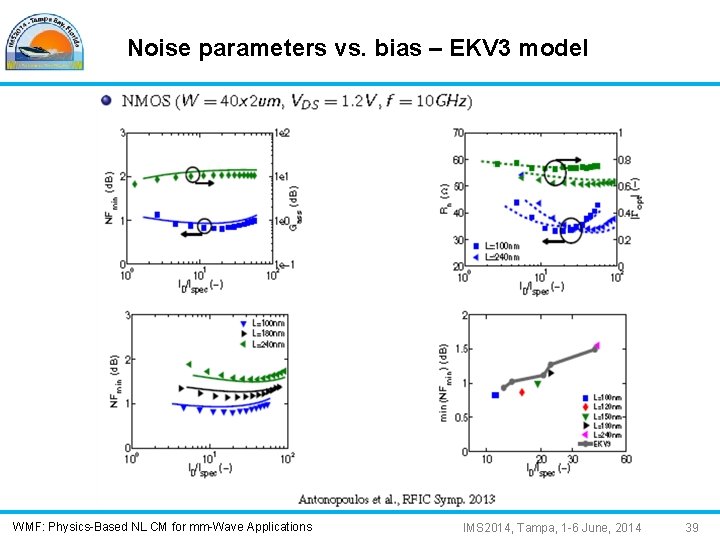
Noise parameters vs. bias – EKV 3 model WMF: Physics-Based NL CM for mm-Wave Applications IMS 2014, Tampa, 1 -6 June, 2014 39
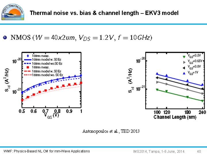
Thermal noise vs. bias & channel length – EKV 3 model WMF: Physics-Based NL CM for mm-Wave Applications IMS 2014, Tampa, 1 -6 June, 2014 40
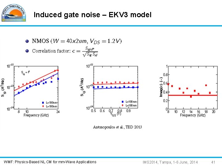
Induced gate noise – EKV 3 model WMF: Physics-Based NL CM for mm-Wave Applications IMS 2014, Tampa, 1 -6 June, 2014 41
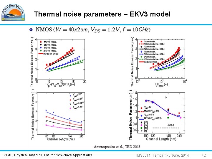
Thermal noise parameters – EKV 3 model WMF: Physics-Based NL CM for mm-Wave Applications IMS 2014, Tampa, 1 -6 June, 2014 42
Conclusions • EKV 3: analog/RF IC design-oriented, charge-based, compact model • Model covers all aspects from DC to RF – – Fully scalable with L, W, NF, bias, f, technology Small/large signal including NQS Noise Simple model structure & parameter extraction • RF model validations – Vs. measurements in 180 – 110 – 90 – 65 nm CMOS. – Vs. TCAD to 22 nm CMOS. – Implementations in: Spectre, ELDO, Smash, HSPICE (underway) WMF: Physics-Based NL CM for mm-Wave Applications IMS 2014, Tampa, 1 -6 June, 2014 43
Conclusions • Relation to advanced analog/RF IC design – Trend towards moderate inversion: optimum Gm/ID. FT, best noise/gain/linearity performance • Optimal RF CMOS (for LV-LP RFIC) performance shifted to lower levels of inversion (near-threshold) with CMOS technology approaching 22 nm. • EKV 3 model incorporates all necessary short-channel effects for correct RF Noise at mm-waves. WMF: Physics-Based NL CM for mm-Wave Applications IMS 2014, Tampa, 1 -6 June, 2014 44
EKV 3 publications EKV 3 model, RFCMOS papers – A. Antonopoulos, M. Bucher, K. Papathanasiou, N. Mavredakis, N. Makris, R. K. Sharma, P. Sakalas, M. Schroter, Small-Signal and Thermal Noise Compact Modelling at High Frequencies, IEEE Trans. Electron Devices, Vol. 60, N° 11, pp. 3726 -3733, Nov. 2013. – A. Antonopoulos, M. Bucher, K. Papathanasiou, N. Makris, N. Mavredakis, R. K. Sharma, P. Sakalas, M. Schroter, Modeling of High Frequency Noise of Silicon CMOS Transistors for RFIC Design, International Journal of Numerical Modelling, 2014. – A. Antonopoulos, M. Bucher, K. Papathanasiou, N. Makris, R. K. Sharma, P. Sakalas, M. Schroter, CMOS RF Noise, Scaling, and Compact Modeling for RFIC Design, Proc. IEEE Radio Frequency Integrated Circuits Symposium (RFIC), Seattle, Washington, June 2 -4, 2013. – S. Yoshitomi, A. Bazigos, M. Bucher, The EKV 3 Model Parameter Extraction and Characterization of 90 nm RF-CMOS Technology, 14 th Int. Conf. on Mixed Design of Integrated Circuits and Systems (MIXDES), pp. 74 -79, Ciechocinek, Poland, June 21 -23, 2007. – M. Bucher, A. Bazigos, S. Yoshitomi, N. Itoh, A Scalable Advanced RF IC Design-Oriented MOSFET Model, Int. Journal of RF and Microwave Computer Aided Engineering, Vol. 18, N° 4, pp. 314 -325, 2008. – M. Bucher, A. Bazigos, An Efficient Channel Segmentation Approach for a Large-Signal NQS MOSFET Model, Solid-State Electronics, Vol. 52, N° 2, pp. 275 -281, Feb. 2008. WMF: Physics-Based NL CM for mm-Wave Applications IMS 2014, Tampa, 1 -6 June, 2014 45
EKV 3 publications EKV 3 model, general papers – K. Papathanasiou, N. Makris, A. Antonopoulos, M. Bucher, Moderate inversion: analogue and RF benchmarking of the EKV 3 compact model, 29 th Int. Conf. on Microelectronics (MIEL), Belgrade, Serbia, May 12 -15, 2014. – C. Enz, E. Vittoz, Charge-based MOS Transistor Modeling, The EKV model for lowpower and RF IC design, Wiley, 2006. – J. -M. Sallese, M. Bucher, F. Krummenacher, P. Fazan, Inversion Charge Linearization in MOSFET Modeling and Rigorous Derivation of the EKV Compact Model, Solid-State Electronics, Vol. 47, N° 4, pp. 677 -683, Apr. 2003 WMF: Physics-Based NL CM for mm-Wave Applications IMS 2014, Tampa, 1 -6 June, 2014 46
Thank you for your attention • Acknowledgments: • Contact: bucher@electronics. tuc. gr Electonic and Computer Engineering Technical University of Crete Chania 73100, Greece WMF: Physics-Based NL CM for mm-Wave Applications IMS 2014, Tampa, 1 -6 June, 2014 47
- Slides: 47