
COMP 411 Computer Organization Transistors and Logic Part
- Slides: 38
COMP 411: Computer Organization Transistors and Logic, Part 1 Don Porter 1
COMP 411: Computer Organization Today’s Topics • Where are we in this course? • Today’s topics – Why go digital? – Encoding bits using voltages – Digital design primitives • transistors and gates 2
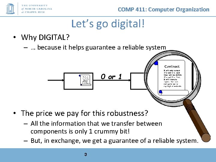
COMP 411: Computer Organization Let’s go digital! • Why DIGITAL? – … because it helps guarantee a reliable system 0 or 1 • The price we pay for this robustness? – All the information that we transfer between components is only 1 crummy bit! – But, in exchange, we get a guarantee of a reliable system. 3
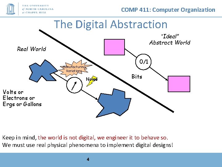
COMP 411: Computer Organization The Digital Abstraction “Ideal” Abstract World Real World 0/1 Manufacturing Variations Noise Bits Volts or Electrons or Ergs or Gallons Keep in mind, the world is not digital, we engineer it to behave so. We must use real physical phenomena to implement digital designs! 4
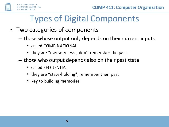
COMP 411: Computer Organization Types of Digital Components • Two categories of components – those whose output only depends on their current inputs • called COMBINATIONAL • they are “memory-less”, don’t remember the past – those who output depends also on their past state • called SEQUENTIAL • they are “state-holding”, remember their past • key to building memories 5
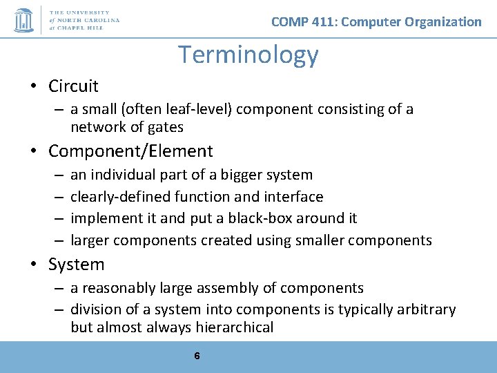
COMP 411: Computer Organization Terminology • Circuit – a small (often leaf-level) component consisting of a network of gates • Component/Element – – an individual part of a bigger system clearly-defined function and interface implement it and put a black-box around it larger components created using smaller components • System – a reasonably large assembly of components – division of a system into components is typically arbitrary but almost always hierarchical 6
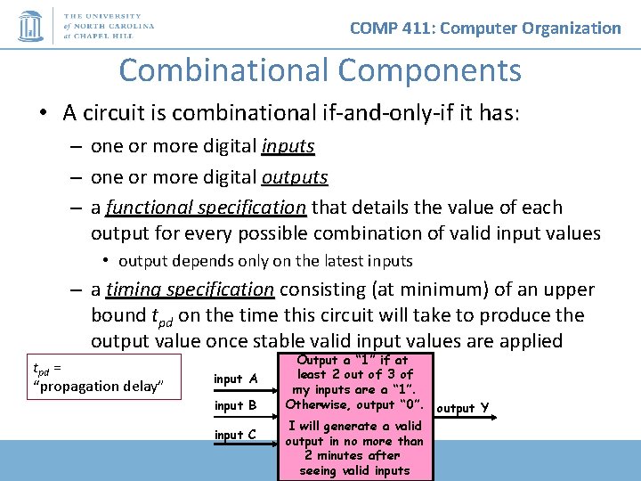
COMP 411: Computer Organization Combinational Components • A circuit is combinational if-and-only-if it has: – – – one or more digital inputs one or more digital outputs a functional specification that details the value of each output for every possible combination of valid input values • output depends only on the latest inputs – a timing specification consisting (at minimum) of an upper bound tpd on the time this circuit will take to produce the output value once stable valid input values are applied tpd = “propagation delay” input A input B input C Output a “ 1” if at least 2 out of 3 of my inputs are a “ 1”. Otherwise, output “ 0”. I will generate a valid output in no more than 2 minutes after seeing valid inputs output Y
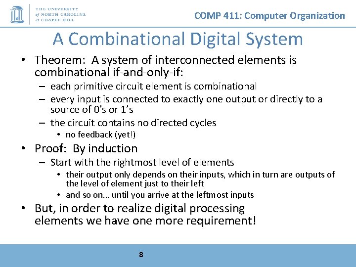
COMP 411: Computer Organization A Combinational Digital System • Theorem: A system of interconnected elements is combinational if-and-only-if: – each primitive circuit element is combinational – every input is connected to exactly one output or directly to a source of 0’s or 1’s – the circuit contains no directed cycles • no feedback (yet!) • Proof: By induction – Start with the rightmost level of elements • their output only depends on their inputs, which in turn are outputs of the level of element just to their left • and so on… until you arrive at the leftmost inputs • But, in order to realize digital processing elements we have one more requirement! 8
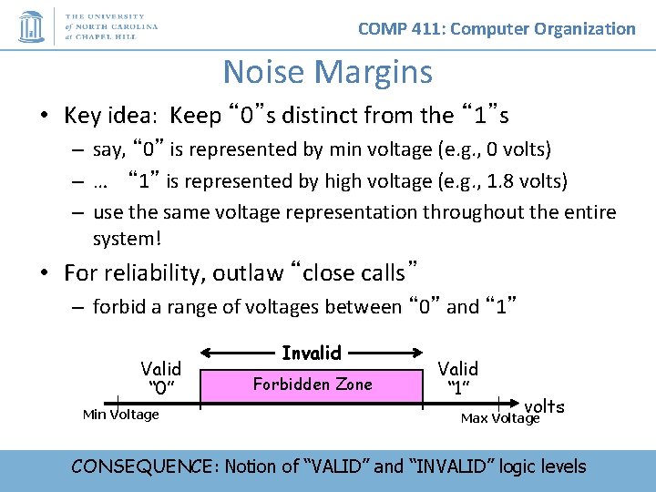
COMP 411: Computer Organization Noise Margins • Key idea: Keep “ 0”s distinct from the “ 1”s – – – say, “ 0” is represented by min voltage (e. g. , 0 volts) … “ 1” is represented by high voltage (e. g. , 1. 8 volts) use the same voltage representation throughout the entire system! • For reliability, outlaw “close calls” – forbid a range of voltages between “ 0” and “ 1” Valid “ 0” Min Voltage Invalid Forbidden Zone Valid “ 1” volts Max Voltage CONSEQUENCE: Notion of “VALID” and “INVALID” logic levels
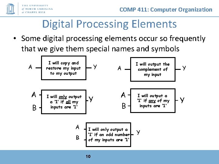
COMP 411: Computer Organization Digital Processing Elements • Some digital processing elements occur so frequently that we give them special names and symbols A A B I will copy and restore my input tobuffer my output I will only output a ‘ 1’AND if all my inputs are ‘ 1’ A B Y A I will output the complement of my input Y inverter Y A B I will only output a ‘ 1’ if an XOR odd number of my inputs are ‘ 1’ 10 I will output a ‘ 1’ if any OR of my inputs are ‘ 1’ Y Y
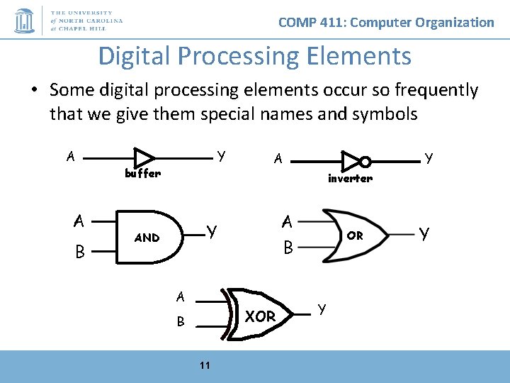
COMP 411: Computer Organization Digital Processing Elements • Some digital processing elements occur so frequently that we give them special names and symbols A Y buffer A B A Y inverter A B Y AND A XOR B 11 OR Y Y
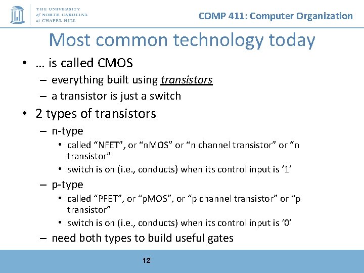
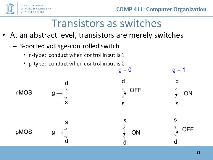
COMP 411: Computer Organization Most common technology today • … is called CMOS – everything built using transistors – a transistor is just a switch • 2 types of transistors – n-type • called “NFET”, or “n. MOS” or “n channel transistor” or “n transistor” • switch is on (i. e. , conducts) when its control input is ‘ 1’ – p-type • called “PFET”, or “p. MOS”, or “p channel transistor” or “p transistor” • switch is on (i. e. , conducts) when its control input is ‘ 0’ – need both types to build useful gates 12
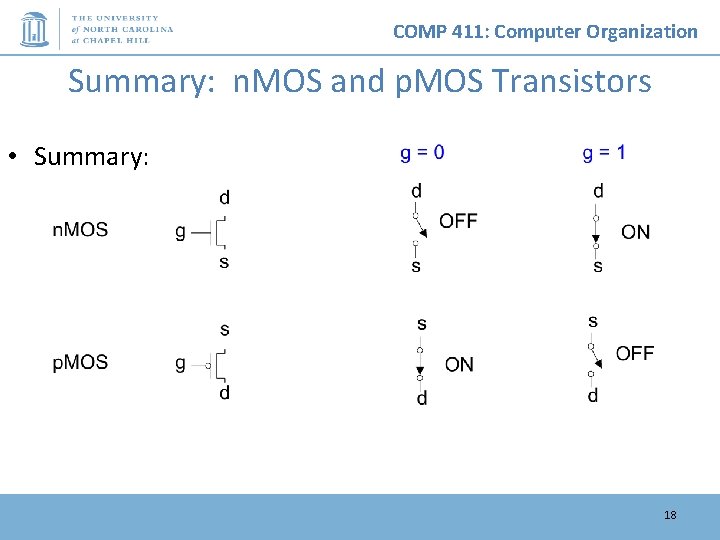
COMP 411: Computer Organization Transistors as switches • At an abstract level, transistors are merely switches – 3 -ported voltage-controlled switch • n-type: conduct when control input is 1 • p-type: conduct when control input is 0 13
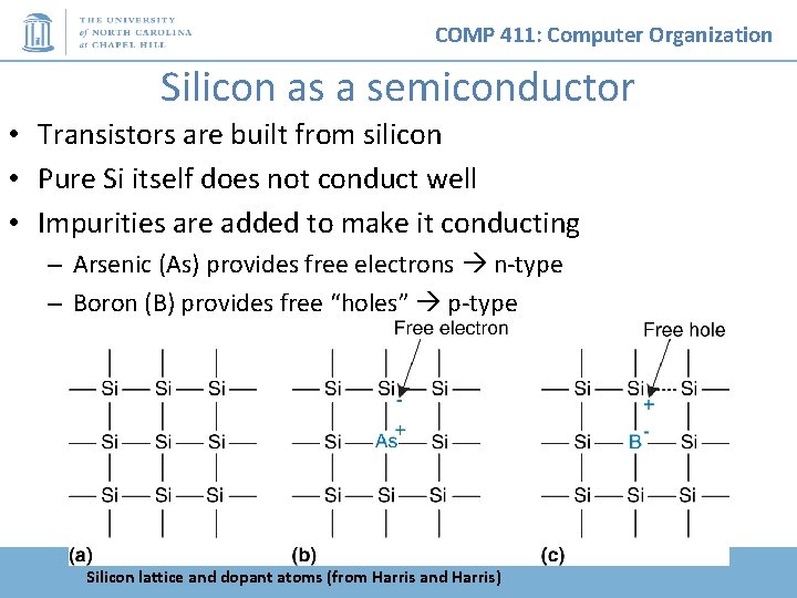
COMP 411: Computer Organization Silicon as a semiconductor • Transistors are built from silicon • Pure Si itself does not conduct well • Impurities are added to make it conducting – Arsenic (As) provides free electrons n-type – Boron (B) provides free “holes” p-type Silicon lattice and dopant atoms (from Harris and Harris)
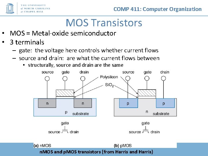
COMP 411: Computer Organization MOS Transistors • MOS = Metal-oxide semiconductor • 3 terminals – gate: the voltage here controls whether current flows – source and drain: are what the current flows between • structurally, source and drain are the same n. MOS and p. MOS transistors (from Harris and Harris)
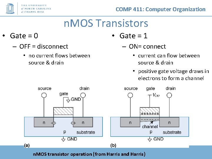
COMP 411: Computer Organization n. MOS Transistors • Gate = 0 – OFF = disconnect • no current flows between source & drain • Gate = 1 – ON= connect • current can flow between source & drain • positive gate voltage draws in electrons to form a channel n. MOS transistor operation (from Harris and Harris)
COMP 411: Computer Organization p. MOS Transistors • Just the opposite – Gate = 1 disconnect – Gate = 0 connect 17
COMP 411: Computer Organization Summary: n. MOS and p. MOS Transistors • Summary: 18
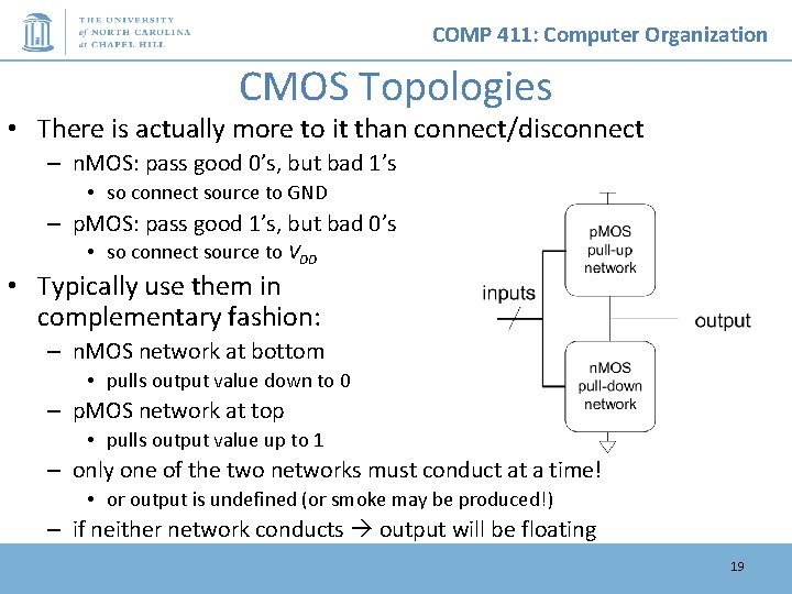
COMP 411: Computer Organization CMOS Topologies • There is actually more to it than connect/disconnect – n. MOS: pass good 0’s, but bad 1’s • so connect source to GND – p. MOS: pass good 1’s, but bad 0’s • so connect source to VDD • Typically use them in complementary fashion: – n. MOS network at bottom • pulls output value down to 0 – p. MOS network at top • pulls output value up to 1 – only one of the two networks must conduct at a time! • or output is undefined (or smoke may be produced!) – if neither network conducts output will be floating 19
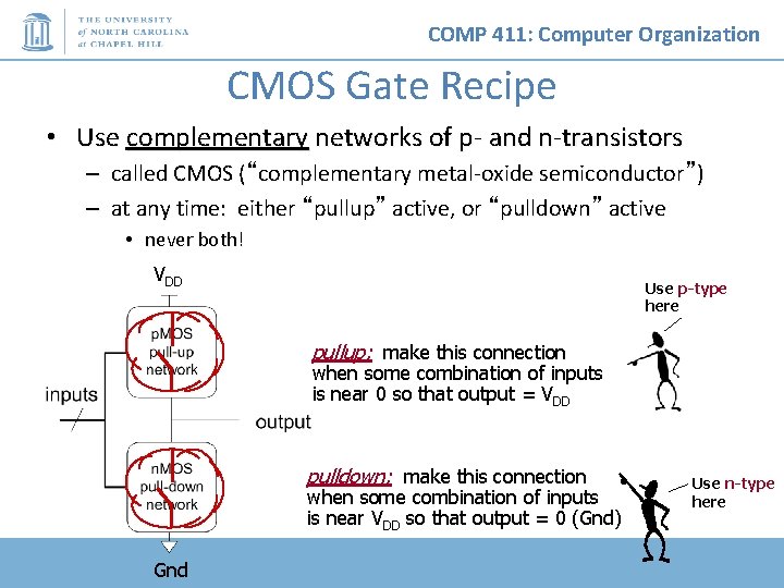
COMP 411: Computer Organization CMOS Gate Recipe • Use complementary networks of p- and n-transistors – called CMOS (“complementary metal-oxide semiconductor”) – at any time: either “pullup” active, or “pulldown” active • never both! VDD Use p-type here pullup: make this connection when some combination of inputs is near 0 so that output = VDD pulldown: make this connection when some combination of inputs is near VDD so that output = 0 (Gnd) Gnd Use n-type here
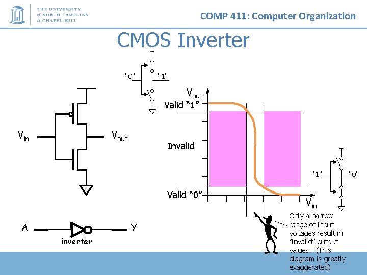
COMP 411: Computer Organization CMOS Inverter “ 0” “ 1” Vout Valid “ 1” Vin Vout Invalid “ 1” Valid “ 0” A Y inverter Vin Only a narrow range of input voltages result in “invalid” output values. (This diagram is greatly exaggerated) “ 0”
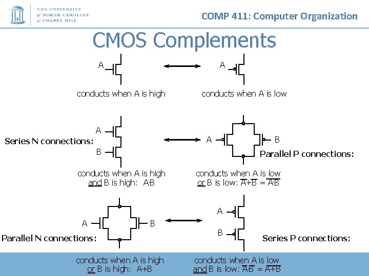
COMP 411: Computer Organization CMOS Complements A A conducts when A is high A conducts when A is low A Series N connections: B B Parallel P connections: conducts when A is high and B is high: A. B conducts when A is low or B is low: A+B = A. B A A B Parallel N connections: conducts when A is high or B is high: A+B B Series P connections: conducts when A is low and B is low: A. B = A+B
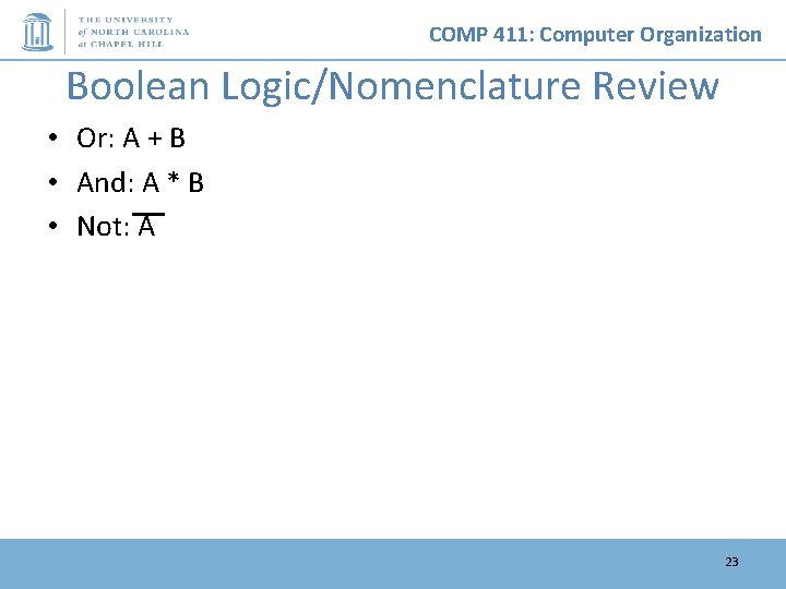
COMP 411: Computer Organization Boolean Logic/Nomenclature Review • Or: A + B • And: A * B • Not: A 23
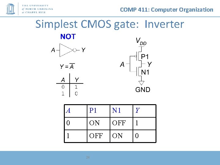
COMP 411: Computer Organization Simplest CMOS gate: Inverter A P 1 N 1 Y 0 ON OFF 1 1 OFF ON 0 24
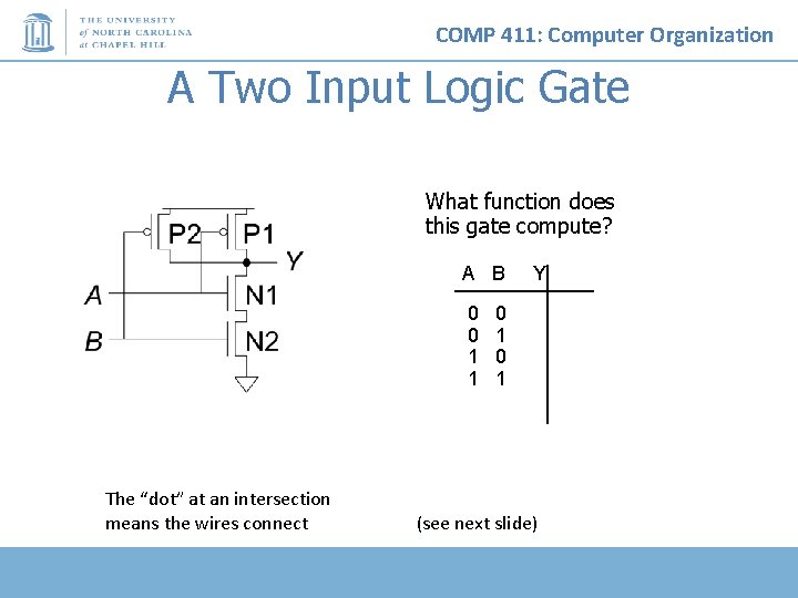
COMP 411: Computer Organization A Two Input Logic Gate What function does this gate compute? A B 0 0 1 1 The “dot” at an intersection means the wires connect Y 0 1 (see next slide)
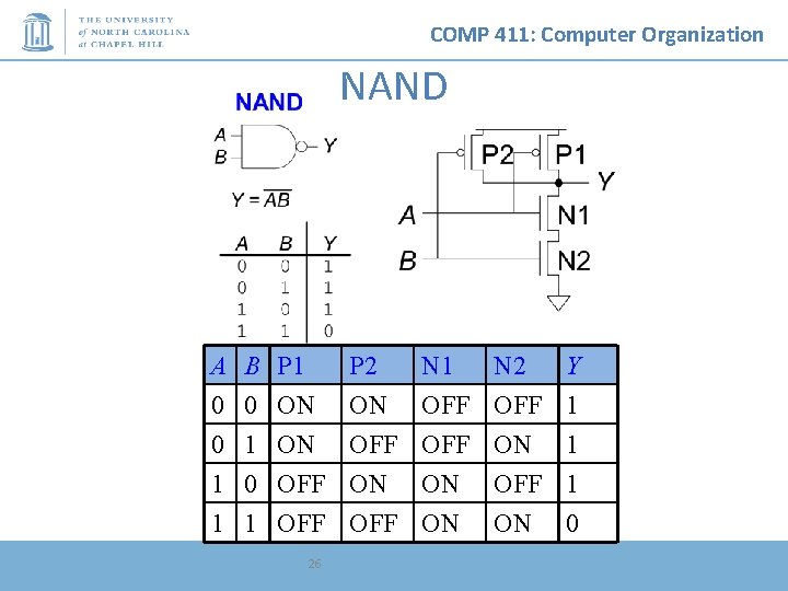
COMP 411: Computer Organization NAND A 0 0 1 B 0 1 0 P 1 ON ON OFF P 2 ON OFF ON N 1 OFF ON 1 1 OFF ON 26 N 2 OFF ON OFF Y 1 1 1 ON 0
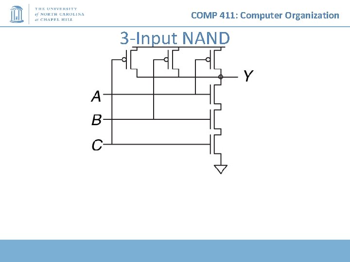
COMP 411: Computer Organization 3 -Input NAND
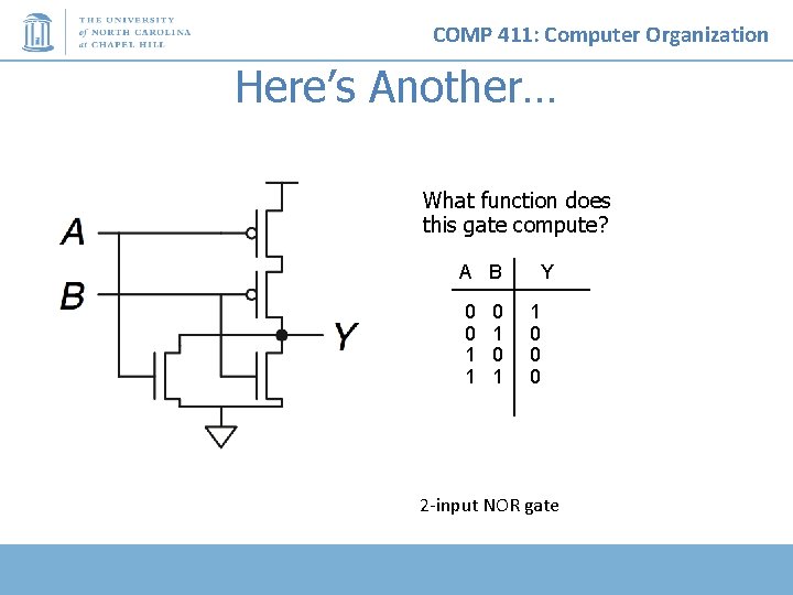
COMP 411: Computer Organization Here’s Another… What function does this gate compute? A B 0 0 1 1 0 1 Y 1 0 0 0 2 -input NOR gate
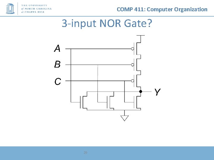
COMP 411: Computer Organization 3 -input NOR Gate? 29
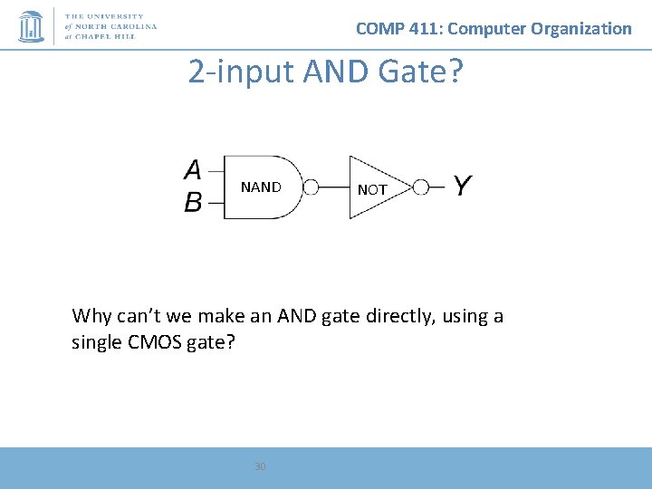
COMP 411: Computer Organization 2 -input AND Gate? NAND NOT Why can’t we make an AND gate directly, using a single CMOS gate? 30
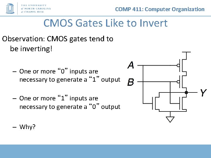
COMP 411: Computer Organization CMOS Gates Like to Invert Observation: CMOS gates tend to be inverting! – One or more “ 0” inputs are necessary to generate a “ 1” output – One or more “ 1” inputs are necessary to generate a “ 0” output – Why?
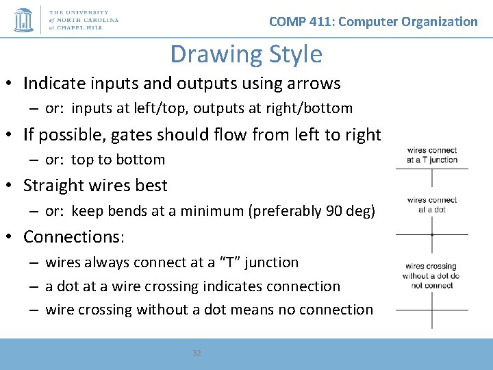
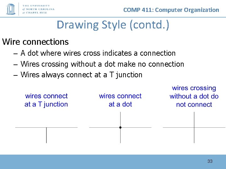
COMP 411: Computer Organization Drawing Style • Indicate inputs and outputs using arrows – or: inputs at left/top, outputs at right/bottom • If possible, gates should flow from left to right – or: top to bottom • Straight wires best – or: keep bends at a minimum (preferably 90 deg) • Connections: – wires always connect at a “T” junction – a dot at a wire crossing indicates connection – wire crossing without a dot means no connection 32
COMP 411: Computer Organization Drawing Style (contd. ) Wire connections – A dot where wires cross indicates a connection – Wires crossing without a dot make no connection – Wires always connect at a T junction 33
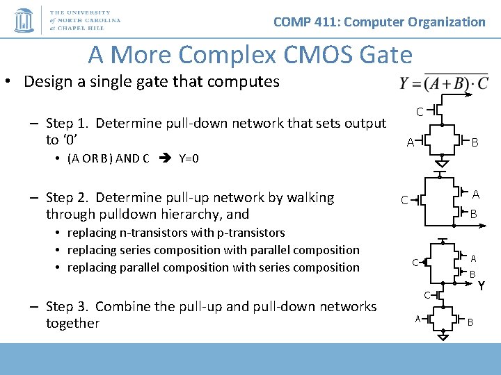
COMP 411: Computer Organization A More Complex CMOS Gate • Design a single gate that computes – Step 1. Determine pull-down network that sets output to ‘ 0’ C A B • (A OR B) AND C Y=0 – Step 2. Determine pull-up network by walking through pulldown hierarchy, and • replacing n-transistors with p-transistors • replacing series composition with parallel composition • replacing parallel composition with series composition – Step 3. Combine the pull-up and pull-down networks together A C B C A B Y
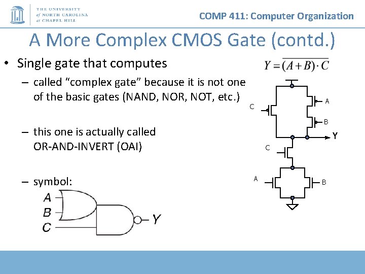
COMP 411: Computer Organization A More Complex CMOS Gate (contd. ) • Single gate that computes – called “complex gate” because it is not one of the basic gates (NAND, NOR, NOT, etc. ) B – this one is actually called OR-AND-INVERT (OAI) – symbol: A C Y C A B
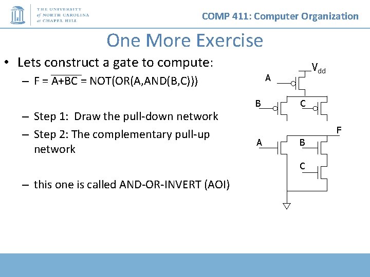
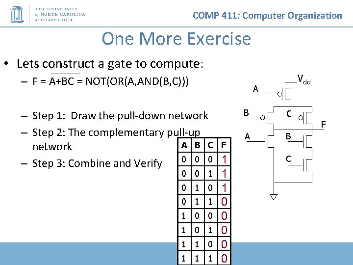
COMP 411: Computer Organization One More Exercise • Lets construct a gate to compute: A – F = A+BC = NOT(OR(A, AND(B, C))) B – Step 1: Draw the pull-down network – Step 2: The complementary pull-up network Vdd C F A B C – this one is called AND-OR-INVERT (AOI)
COMP 411: Computer Organization One More Exercise • Lets construct a gate to compute: – F = A+BC = NOT(OR(A, AND(B, C))) – Step 1: Draw the pull-down network – Step 2: The complementary pull-up A B C F network 0 0 0 1 – Step 3: Combine and Verify 0 0 1 1 0 1 0 1 0 0 0 1 0 1 1 0 0 1 1 1 0 Vdd A B C F A B C
COMP 411: Computer Organization Next • This lecture – basics of transistors – CMOS gates • Next lecture – Boolean algebra – gate-level design 38