COMP 2121 Microprocessors and Interfacing Interrupts http www

- Slides: 86

COMP 2121: Microprocessors and Interfacing Interrupts http: //www. cse. unsw. edu. au/~cs 2121 Lecturer: Hui Wu Session 2, 2017

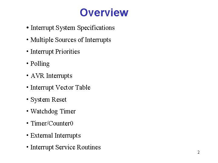
Overview • Interrupt System Specifications • Multiple Sources of Interrupts • Interrupt Priorities • Polling • AVR Interrupts • Interrupt Vector Table • System Reset • Watchdog Timer • Timer/Counter 0 • External Interrupts • Interrupt Service Routines 2

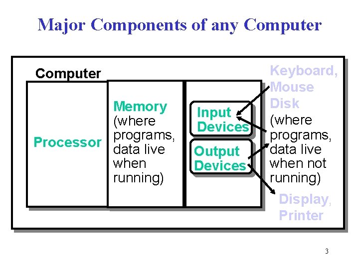
Major Components of any Computer Memory (where programs, Processor data live when running) Input Devices Output Devices Keyboard, Mouse Disk (where programs, data live when not running) Display, Printer 3

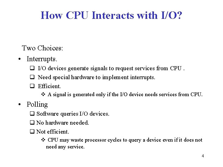
How CPU Interacts with I/O? Two Choices: • Interrupts. q I/O devices generate signals to request services from CPU. q Need special hardware to implement interrupts. q Efficient. v A signal is generated only if the I/O device needs services from CPU. • Polling q Software queries I/O devices. q No hardware needed. q Not efficient. v CPU may waste processor cycles to query a device even if it does not need any service. 4

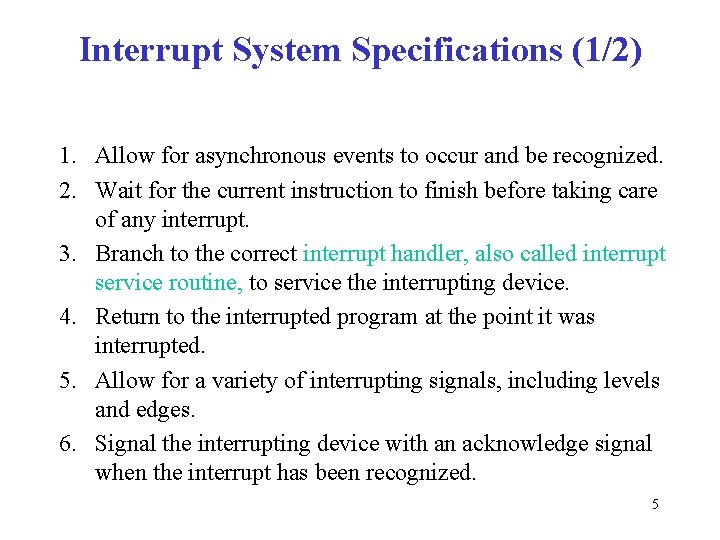
Interrupt System Specifications (1/2) 1. Allow for asynchronous events to occur and be recognized. 2. Wait for the current instruction to finish before taking care of any interrupt. 3. Branch to the correct interrupt handler, also called interrupt service routine, to service the interrupting device. 4. Return to the interrupted program at the point it was interrupted. 5. Allow for a variety of interrupting signals, including levels and edges. 6. Signal the interrupting device with an acknowledge signal when the interrupt has been recognized. 5

Interrupt System Specifications (2/2) 7. Allow programmers to selectively enable and disable all interrupts. 8. Allow programmers to enable and disable selected interrupts. 9. Disable further interrupts while the first is being serviced 10. Deal with multiple sources of interrupts. 11. Deal with multiple, simultaneous interrupts. 6

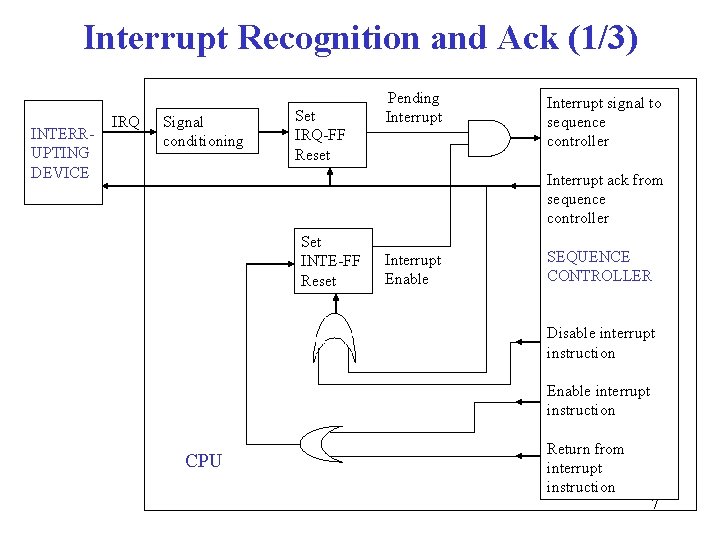
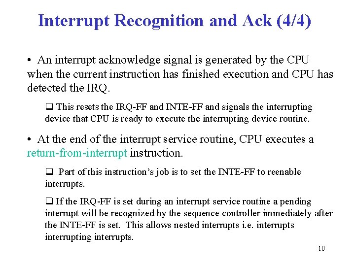
Interrupt Recognition and Ack (1/3) INTERRUPTING DEVICE IRQ Signal conditioning Set IRQ-FF Reset Pending Interrupt signal to sequence controller Interrupt ack from sequence controller Set INTE-FF Reset Interrupt Enable SEQUENCE CONTROLLER Disable interrupt instruction Enable interrupt instruction CPU Return from interrupt instruction 7

Interrupt Recognition and Ack (2/4) • An Interrupt Request (IRQ) may occur at any time. q It may have rising or falling edges or high or low levels. q Frequently it is a active-low signal and multiple devices are wire. ORed together. • Signal Conditioning Circuit detects these different types of signals. • Interrupt Request Flip-Flop (IRQ-FF) remembers that an interrupt request has been generated until it is acknowledged. q When IRQ-FF is set, it generates a pending interrupt signal that goes towards the Sequence Controller. q IRQ-FF is reset when CPU acknowledges the interrupt with INTA signal. 8

Interrupt Recognition and Ack (3/4) • The programmer has control over interrupting process by enabling and disabling interrupts with explicit instructions q The hardware that allows this is Interrupt Enable Flip-Flop (INTE-FF). q When the INTE-FF is set, all interrupts are enabled and the pending interrupt is allowed through the AND gate to the sequence controller. q The INTE-FF is reset in the following cases. v CPU acknowledges the interrupt. v CPU is reset. v Disable interrupt instruction is executed. 9

Interrupt Recognition and Ack (4/4) • An interrupt acknowledge signal is generated by the CPU when the current instruction has finished execution and CPU has detected the IRQ. q This resets the IRQ-FF and INTE-FF and signals the interrupting device that CPU is ready to execute the interrupting device routine. • At the end of the interrupt service routine, CPU executes a return-from-interrupt instruction. q Part of this instruction’s job is to set the INTE-FF to reenable interrupts. q If the IRQ-FF is set during an interrupt service routine a pending interrupt will be recognized by the sequence controller immediately after the INTE-FF is set. This allows nested interrupts i. e. interrupts interrupting interrupts. 10

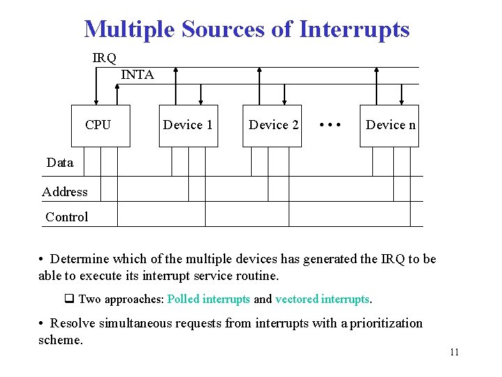
Multiple Sources of Interrupts IRQ INTA CPU Device 1 Device 2 • • • Device n Data Address Control • Determine which of the multiple devices has generated the IRQ to be able to execute its interrupt service routine. q Two approaches: Polled interrupts and vectored interrupts. • Resolve simultaneous requests from interrupts with a prioritization scheme. 11

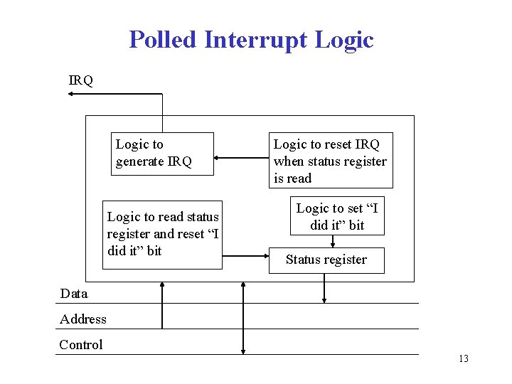
Polled Interrupts • Software, instead of hardware, is responsible for determining the interrupting device. q The device must have logic to generate the IRQ signal and to set an “I did it” bit in a status register that is read by CPU. q The bit is reset after the register has been read. • IRQ signals the sequence controller to start executing an interrupt service routine that first polls the device then branches to the correct service routine. 12

Polled Interrupt Logic IRQ Logic to generate IRQ Logic to read status register and reset “I did it” bit Logic to reset IRQ when status register is read Logic to set “I did it” bit Status register Data Address Control 13

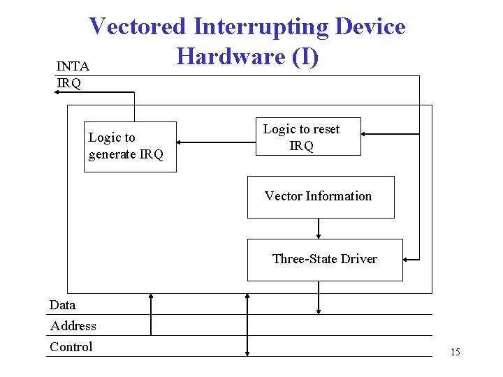
Vectored Interrupts (I) • CPU’s response to IRQ is to assert INTA. • The interrupting device uses INTA to place information that identifies itself, called vector, onto the data bus for CPU to read. q An vector is the address of an interrupt service routine. • CPU uses the vector to execute the interrupt service routine. 14

Vectored Interrupting Device Hardware (I) INTA IRQ Logic to generate IRQ Logic to reset IRQ Vector Information Three-State Driver Data Address Control 15

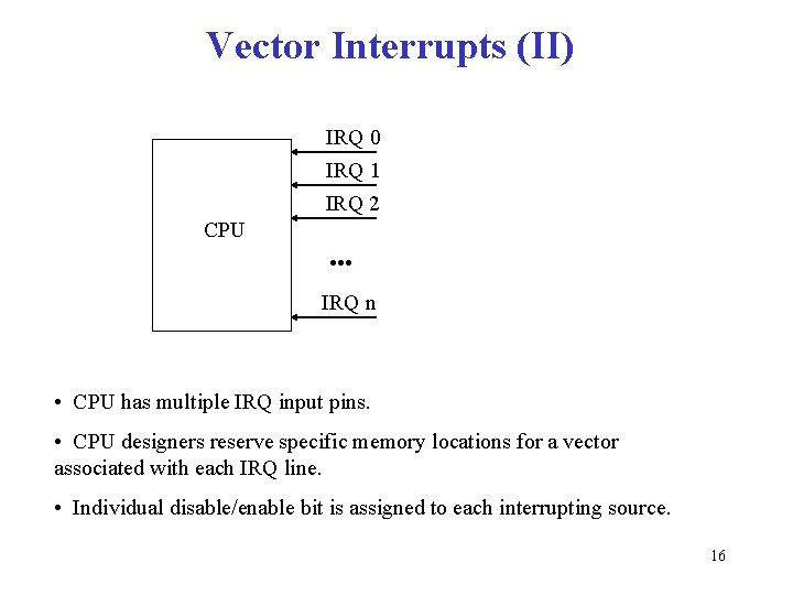
Vector Interrupts (II) IRQ 0 IRQ 1 IRQ 2 CPU • • • IRQ n • CPU has multiple IRQ input pins. • CPU designers reserve specific memory locations for a vector associated with each IRQ line. • Individual disable/enable bit is assigned to each interrupting source. 16

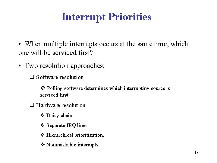
Interrupt Priorities • When multiple interrupts occurs at the same time, which one will be serviced first? • Two resolution approaches: q Software resolution v Polling software determines which interrupting source is serviced first. q Hardware resolution v Daisy chain. v Separate IRQ lines. v Hierarchical prioritization. v Nonmaskable interrupts. 17

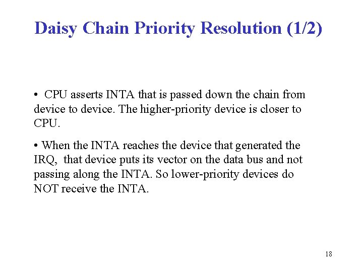
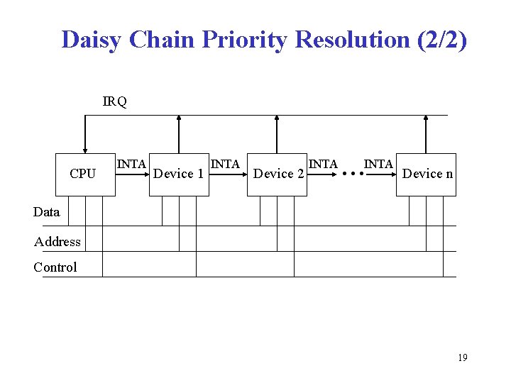
Daisy Chain Priority Resolution (1/2) • CPU asserts INTA that is passed down the chain from device to device. The higher-priority device is closer to CPU. • When the INTA reaches the device that generated the IRQ, that device puts its vector on the data bus and not passing along the INTA. So lower-priority devices do NOT receive the INTA. 18

Daisy Chain Priority Resolution (2/2) IRQ CPU INTA Device 1 INTA Device 2 INTA • • • Device n Data Address Control 19

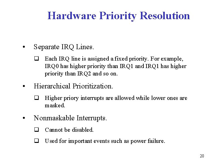
Hardware Priority Resolution • Separate IRQ Lines. q Each IRQ line is assigned a fixed priority. For example, IRQ 0 has higher priority than IRQ 1 and IRQ 1 has higher priority than IRQ 2 and so on. • Hierarchical Prioritization. q Higher priory interrupts are allowed while lower ones are masked. • Nonmaskable Interrupts. q Cannot be disabled. q Used for important events such as power failure. 20

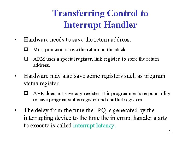
Transferring Control to Interrupt Handler • Hardware needs to save the return address. q Most processors save the return on the stack. q ARM uses a special register, link register, to store the return address. • Hardware may also save some registers such as program status register. q AVR does not save any register. It is programmer’s responsibility to save program status register and conflict registers. • The delay from the time the IRQ is generated by the interrupting device to the time the interrupt handler starts to execute is called interrupt latency. 21

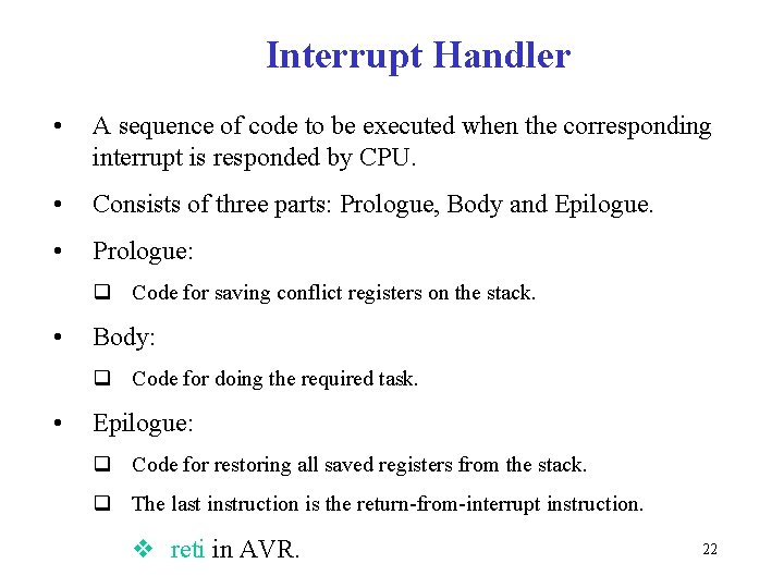
Interrupt Handler • A sequence of code to be executed when the corresponding interrupt is responded by CPU. • Consists of three parts: Prologue, Body and Epilogue. • Prologue: q Code for saving conflict registers on the stack. • Body: q Code for doing the required task. • Epilogue: q Code for restoring all saved registers from the stack. q The last instruction is the return-from-interrupt instruction. v reti in AVR. 22

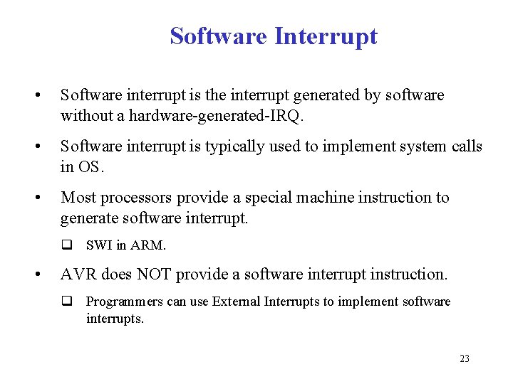
Software Interrupt • Software interrupt is the interrupt generated by software without a hardware-generated-IRQ. • Software interrupt is typically used to implement system calls in OS. • Most processors provide a special machine instruction to generate software interrupt. q SWI in ARM. • AVR does NOT provide a software interrupt instruction. q Programmers can use External Interrupts to implement software interrupts. 23

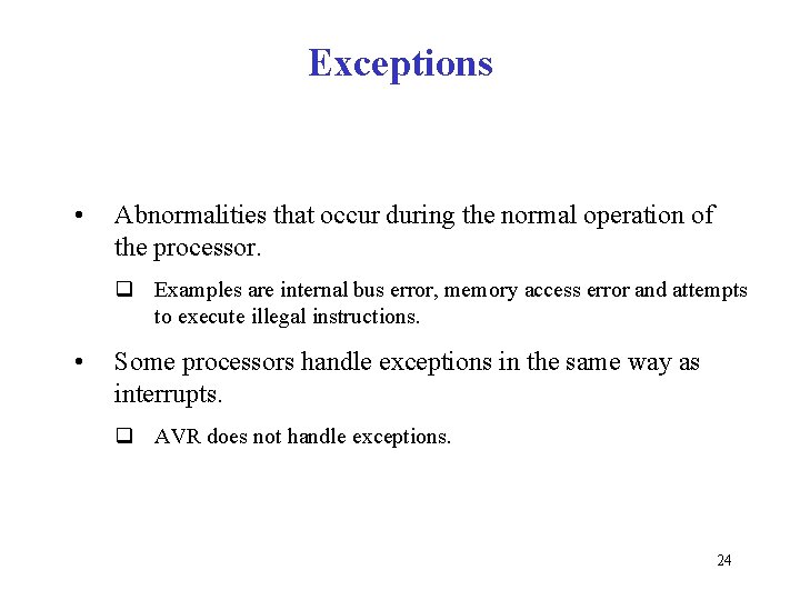
Exceptions • Abnormalities that occur during the normal operation of the processor. q Examples are internal bus error, memory access error and attempts to execute illegal instructions. • Some processors handle exceptions in the same way as interrupts. q AVR does not handle exceptions. 24

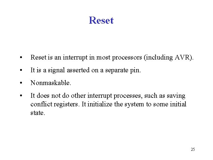
Reset • Reset is an interrupt in most processors (including AVR). • It is a signal asserted on a separate pin. • Nonmaskable. • It does not do other interrupt processes, such as saving conflict registers. It initialize the system to some initial state. 25

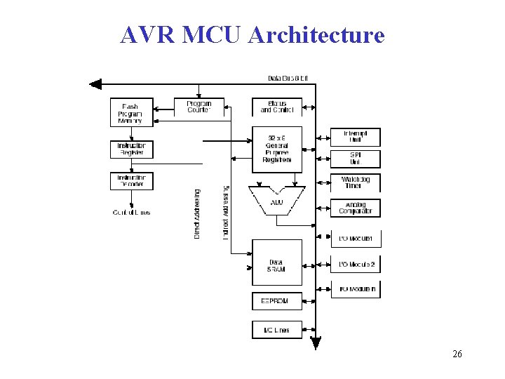
AVR MCU Architecture 26

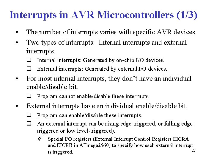
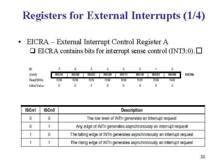
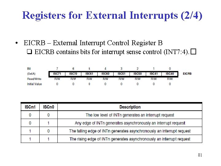
Interrupts in AVR Microcontrollers (1/3) • • The number of interrupts varies with specific AVR devices. Two types of interrupts: Internal interrupts and external interrupts. q Internal interrupts: Generated by on-chip I/O devices. q External interrupts: Generated by external I/O devices. • For most internal interrupts, they don’t have an individual enable/disable bit. q Program cannot enable/disable these interrupts. • External interrupts have an individual enable/disable bit. q Program can enable/disable these interrupts. q An external interrupt can be rising edge-triggered, or falling edgetriggered or low level-triggered). v Special I/O registers (External Interrupt Control Registers EICRA and EICRB in ATmega 2560) to specify how each external interrupt 27 is triggered.

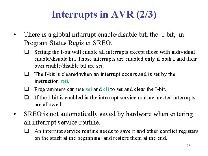
Interrupts in AVR (2/3) • There is a global interrupt enable/disable bit, the I-bit, in Program Status Register SREG. q Setting the I-bit will enable all interrupts except those with individual enable/disable bit. Those interrupts are enabled only if both I and their own enable/disable bit are set. q The I-bit is cleared when an interrupt occurs and is set by the instruction reti. q Programmers can use sei and cli to set and clear the I-bit. q If the I-bit is enabled in the interrupt service routine, nested interrupts are allowed. • SREG is not automatically saved by hardware when entering an interrupt service routine. q An interrupt service routine needs to save it and other conflict registers on the stack at the beginning and restore them at the end. 28

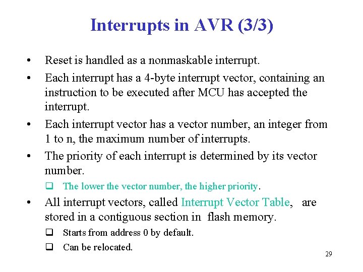
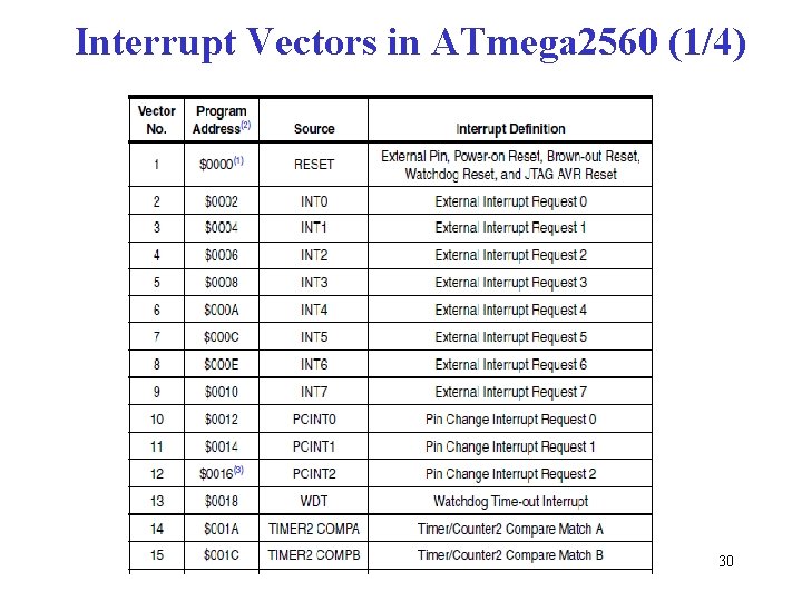
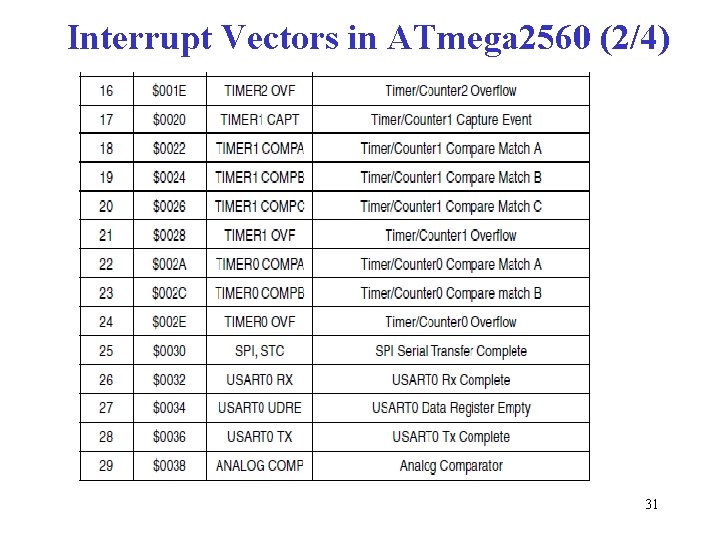
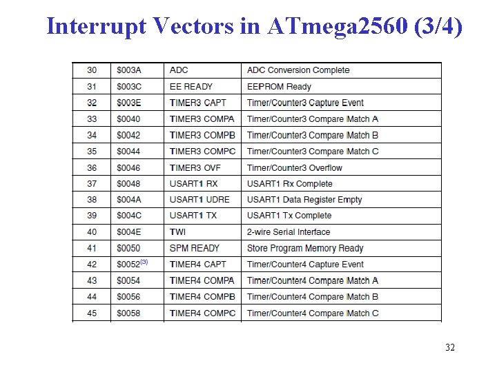
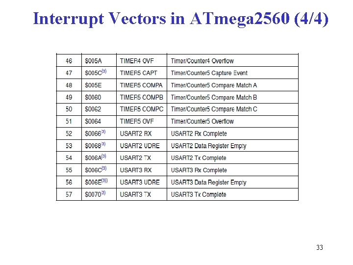
Interrupts in AVR (3/3) • • Reset is handled as a nonmaskable interrupt. Each interrupt has a 4 -byte interrupt vector, containing an instruction to be executed after MCU has accepted the interrupt. Each interrupt vector has a vector number, an integer from 1 to n, the maximum number of interrupts. The priority of each interrupt is determined by its vector number. q The lower the vector number, the higher priority. • All interrupt vectors, called Interrupt Vector Table, are stored in a contiguous section in flash memory. q Starts from address 0 by default. q Can be relocated. 29

Interrupt Vectors in ATmega 2560 (1/4) 30

Interrupt Vectors in ATmega 2560 (2/4) 31

Interrupt Vectors in ATmega 2560 (3/4) 32

Interrupt Vectors in ATmega 2560 (4/4) 33

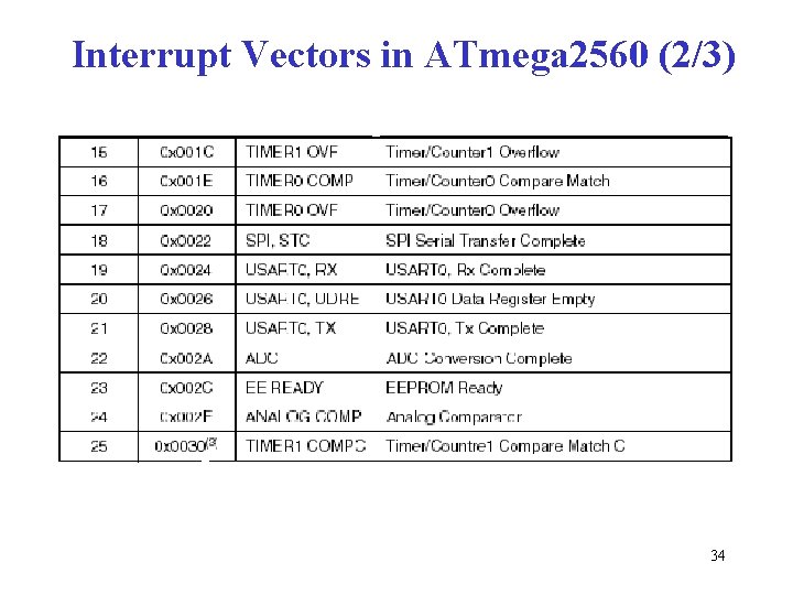
Interrupt Vectors in ATmega 2560 (2/3) 34

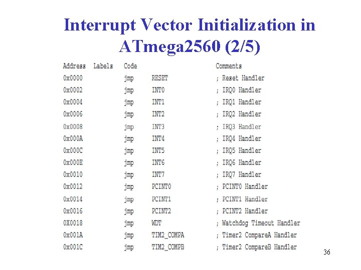
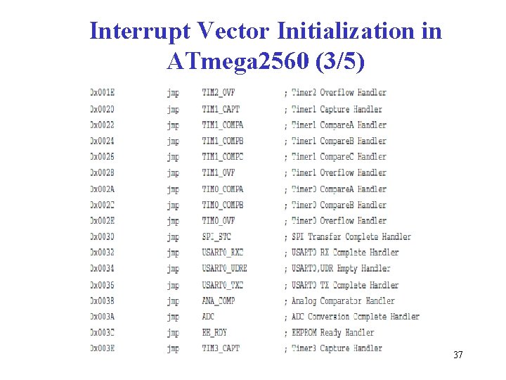
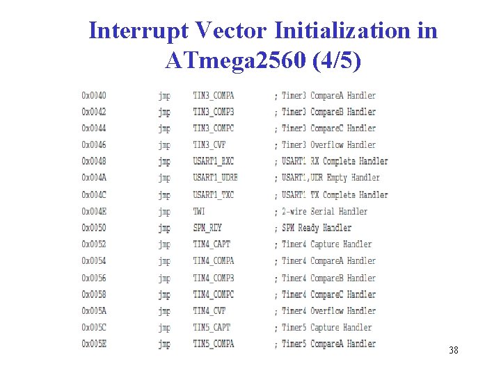
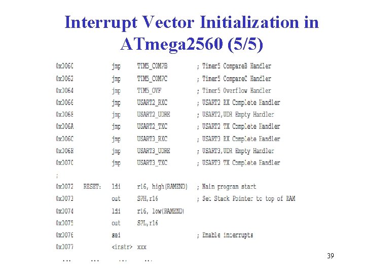
Interrupt Vector Initialization in ATmega 2560 (1/5) • Typically an interrupt vector contains a branch instruction (jmp) that branches to the first instruction of the interrupt handler, or reti (return from interrupt), indicating that this interrupt is not handled. 35

Interrupt Vector Initialization in ATmega 2560 (2/5) 36

Interrupt Vector Initialization in ATmega 2560 (3/5) 37

Interrupt Vector Initialization in ATmega 2560 (4/5) 38

Interrupt Vector Initialization in ATmega 2560 (5/5) 39

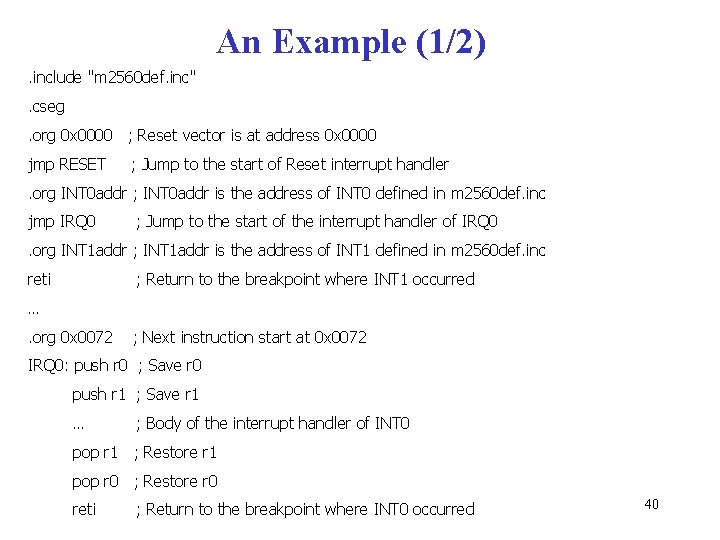
An Example (1/2). include "m 2560 def. inc". cseg. org 0 x 0000 ; Reset vector is at address 0 x 0000 jmp RESET ; Jump to the start of Reset interrupt handler . org INT 0 addr ; INT 0 addr is the address of INT 0 defined in m 2560 def. inc jmp IRQ 0 ; Jump to the start of the interrupt handler of IRQ 0 . org INT 1 addr ; INT 1 addr is the address of INT 1 defined in m 2560 def. inc reti ; Return to the breakpoint where INT 1 occurred …. org 0 x 0072 ; Next instruction start at 0 x 0072 IRQ 0: push r 0 ; Save r 0 push r 1 ; Save r 1 … ; Body of the interrupt handler of INT 0 pop r 1 ; Restore r 1 pop r 0 ; Restore r 0 reti ; Return to the breakpoint where INT 0 occurred 40

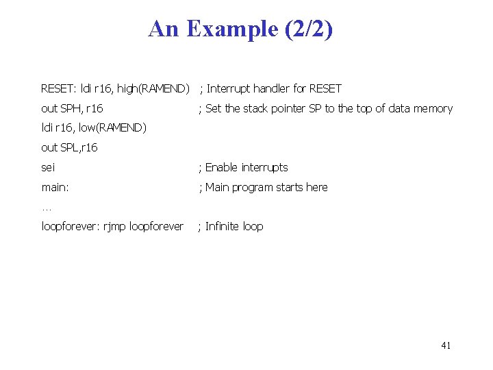
An Example (2/2) RESET: ldi r 16, high(RAMEND) ; Interrupt handler for RESET out SPH, r 16 ; Set the stack pointer SP to the top of data memory ldi r 16, low(RAMEND) out SPL, r 16 sei ; Enable interrupts main: ; Main program starts here … loopforever: rjmp loopforever ; Infinite loop 41

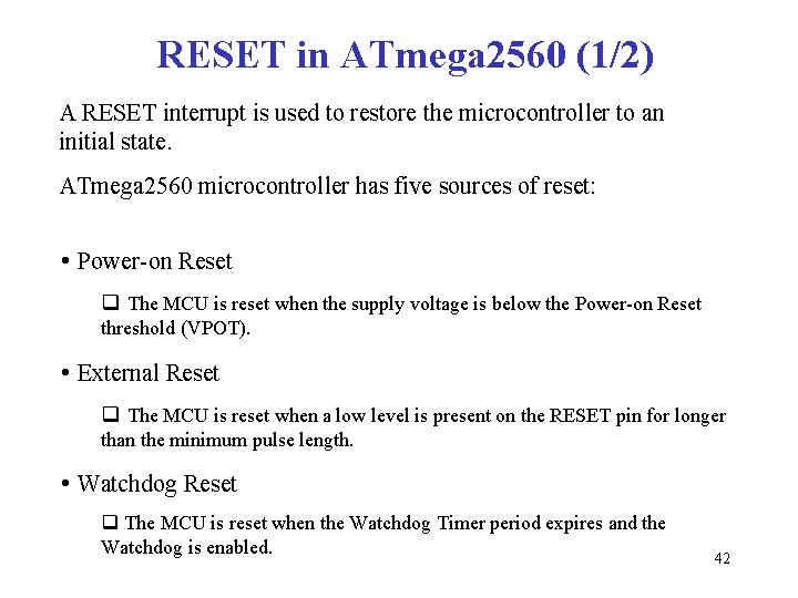
RESET in ATmega 2560 (1/2) A RESET interrupt is used to restore the microcontroller to an initial state. ATmega 2560 microcontroller has five sources of reset: • Power-on Reset q The MCU is reset when the supply voltage is below the Power-on Reset threshold (VPOT). • External Reset q The MCU is reset when a low level is present on the RESET pin for longer than the minimum pulse length. • Watchdog Reset q The MCU is reset when the Watchdog Timer period expires and the Watchdog is enabled. 42

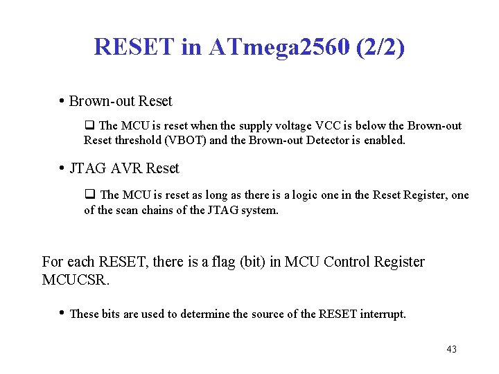
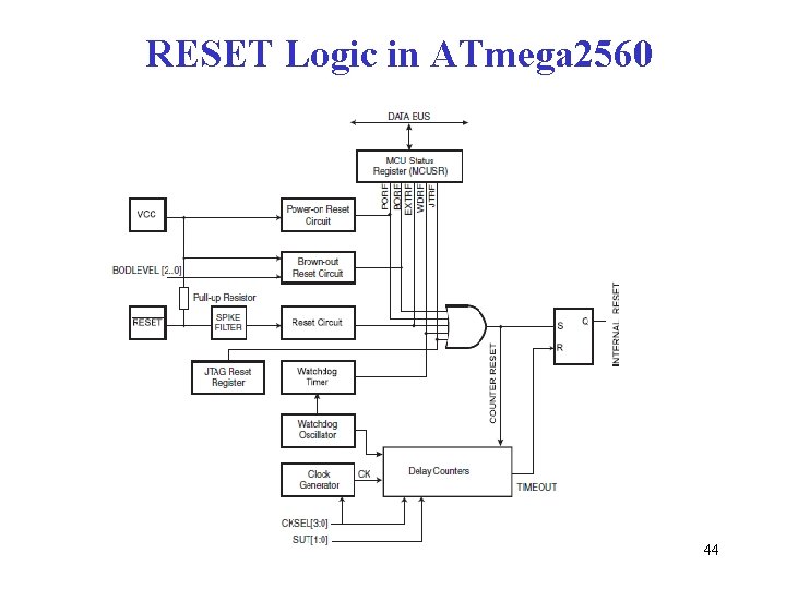
RESET in ATmega 2560 (2/2) • Brown-out Reset q The MCU is reset when the supply voltage VCC is below the Brown-out Reset threshold (VBOT) and the Brown-out Detector is enabled. • JTAG AVR Reset q The MCU is reset as long as there is a logic one in the Reset Register, one of the scan chains of the JTAG system. For each RESET, there is a flag (bit) in MCU Control Register MCUCSR. • These bits are used to determine the source of the RESET interrupt. 43

RESET Logic in ATmega 2560 44

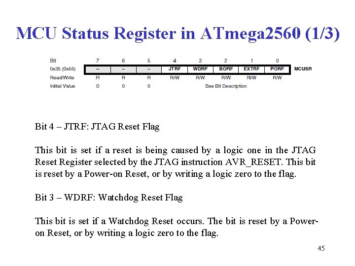
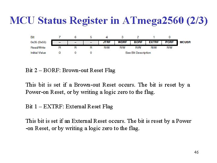
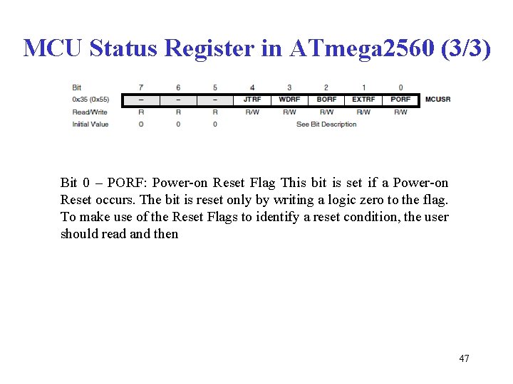
MCU Status Register in ATmega 2560 (1/3) Bit 4 – JTRF: JTAG Reset Flag This bit is set if a reset is being caused by a logic one in the JTAG Reset Register selected by the JTAG instruction AVR_RESET. This bit is reset by a Power-on Reset, or by writing a logic zero to the flag. Bit 3 – WDRF: Watchdog Reset Flag This bit is set if a Watchdog Reset occurs. The bit is reset by a Poweron Reset, or by writing a logic zero to the flag. 45

MCU Status Register in ATmega 2560 (2/3) Bit 2 – BORF: Brown-out Reset Flag This bit is set if a Brown-out Reset occurs. The bit is reset by a Power-on Reset, or by writing a logic zero to the flag. Bit 1 – EXTRF: External Reset Flag This bit is set if an External Reset occurs. The bit is reset by a Power -on Reset, or by writing a logic zero to the flag. 46

MCU Status Register in ATmega 2560 (3/3) Bit 0 – PORF: Power-on Reset Flag This bit is set if a Power-on Reset occurs. The bit is reset only by writing a logic zero to the flag. To make use of the Reset Flags to identify a reset condition, the user should read and then 47

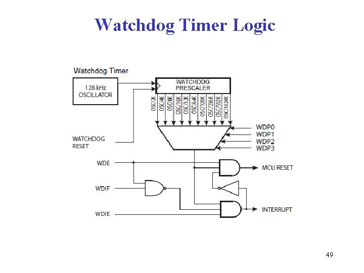
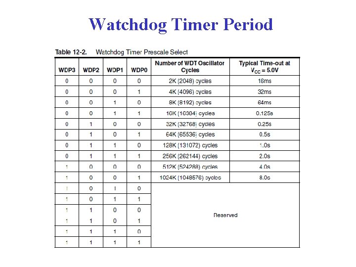
Watchdog Timer in ATmega 2560 • Used to detect software crash. • Can be enabled or disabled by properly updating WDCE bit and WDE bit in Watchdog Timer Control Register WDTCR. • 10 different periods determined by WDP 3, WDP 2, WDP 1 and WDP 0 bits in WDTCR. • If enabled, it generates a Watchdog Reset interrupt when its period expires. • So program needs to reset it before its period expires by executing instruction WDR. • When its period expires, Watchdog Reset Flag WDRF in MCU Control Register MCUCSR is set. q This flag is used to determine if the watchdog timer has generated a RESET interrupt. 48

Watchdog Timer Logic 49

Watchdog Timer Period 50

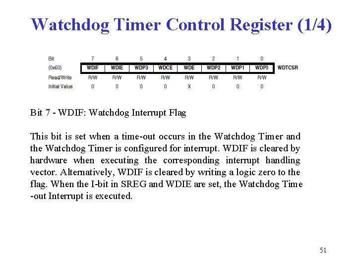
Watchdog Timer Control Register (1/4) Bit 7 - WDIF: Watchdog Interrupt Flag This bit is set when a time-out occurs in the Watchdog Timer and the Watchdog Timer is configured for interrupt. WDIF is cleared by hardware when executing the corresponding interrupt handling vector. Alternatively, WDIF is cleared by writing a logic zero to the flag. When the I-bit in SREG and WDIE are set, the Watchdog Time -out Interrupt is executed. 51

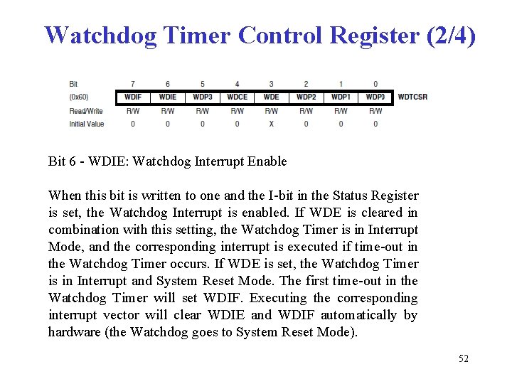
Watchdog Timer Control Register (2/4) Bit 6 - WDIE: Watchdog Interrupt Enable When this bit is written to one and the I-bit in the Status Register is set, the Watchdog Interrupt is enabled. If WDE is cleared in combination with this setting, the Watchdog Timer is in Interrupt Mode, and the corresponding interrupt is executed if time-out in the Watchdog Timer occurs. If WDE is set, the Watchdog Timer is in Interrupt and System Reset Mode. The first time-out in the Watchdog Timer will set WDIF. Executing the corresponding interrupt vector will clear WDIE and WDIF automatically by hardware (the Watchdog goes to System Reset Mode). 52

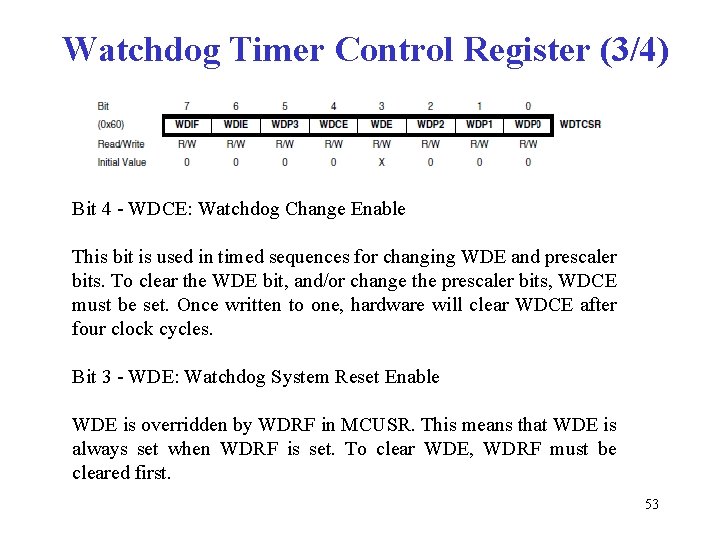
Watchdog Timer Control Register (3/4) Bit 4 - WDCE: Watchdog Change Enable This bit is used in timed sequences for changing WDE and prescaler bits. To clear the WDE bit, and/or change the prescaler bits, WDCE must be set. Once written to one, hardware will clear WDCE after four clock cycles. Bit 3 - WDE: Watchdog System Reset Enable WDE is overridden by WDRF in MCUSR. This means that WDE is always set when WDRF is set. To clear WDE, WDRF must be cleared first. 53

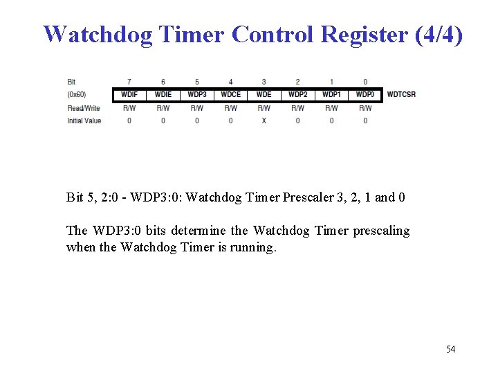
Watchdog Timer Control Register (4/4) Bit 5, 2: 0 - WDP 3: 0: Watchdog Timer Prescaler 3, 2, 1 and 0 The WDP 3: 0 bits determine the Watchdog Timer prescaling when the Watchdog Timer is running. 54

Timer Interrupt (1/2) Timer interrupt has many applications: • Used to schedule (real-time) tasks (threads) q Round-Robin scheduling v All tasks take turn to execute for some fixed period. q Real-time scheduling v Some tasks must be started at a particular time and finished by a deadline. v Some tasks must be periodically executed. • Used to implement a clock q How much time has passed since the system started? 55

Timer Interrupt (2/2) • Used to synchronize tasks. q Task A can be started only if a certain amount of time has passed since the completion of task B. • Can be coupled with a wave-form generator to support Pulse-Width Modulation (PWM). q Details to be covered in the lecture about Analog Input and Output. 56

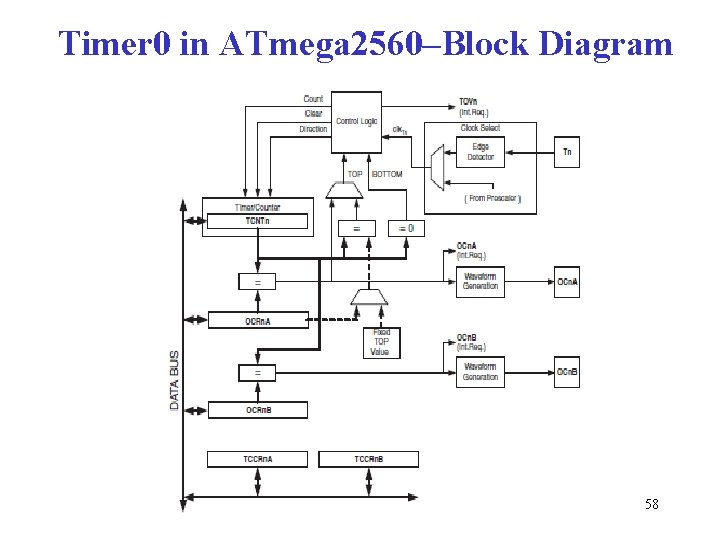
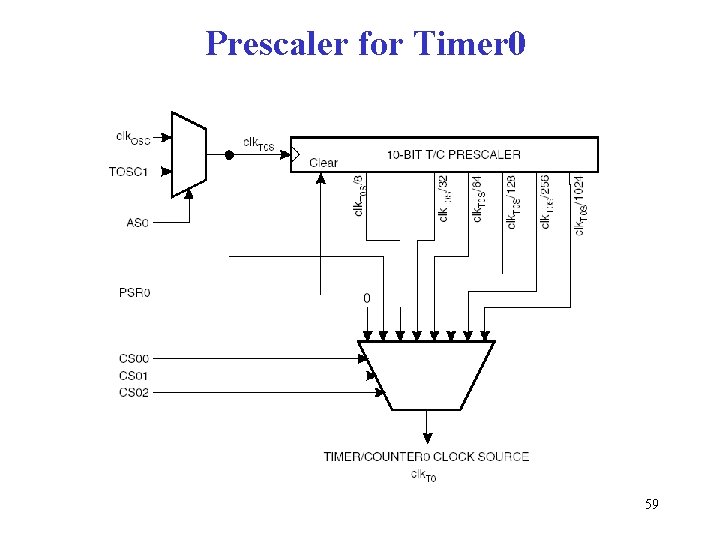
Timer 0 in ATmega 2560 The 8 -bit timer has the following features: • Glitch-free, Phase Correct Pulse Width Modulators (PWM). • 10 -bit Clock Prescaler. • The counter can count up or count down depending on the specific operation mode. • One Overflow Interrupt source (TOV 0) and two Compare Match Interrupt sources (OC 0 A and OC 0 B). q The timer can generate a Timer 0 Overflow Interrupt TOV 0 when the counter TCNT 0 overflows. q The timer can generate two Timer/Counter 0 Output Match Interrupts: Timer/Counter Compare Match A interrupt and Timer/Counter Compare Match B interrupt when TCNT 0 contains the same value as in Output Compare Registers (OCR 0 A and OCR 0 B) q TOV 0 and two Timer/Counter 0 Output Match Interrupts can be individually enabled/disabled. 57

Timer 0 in ATmega 2560–Block Diagram 58

Prescaler for Timer 0 59

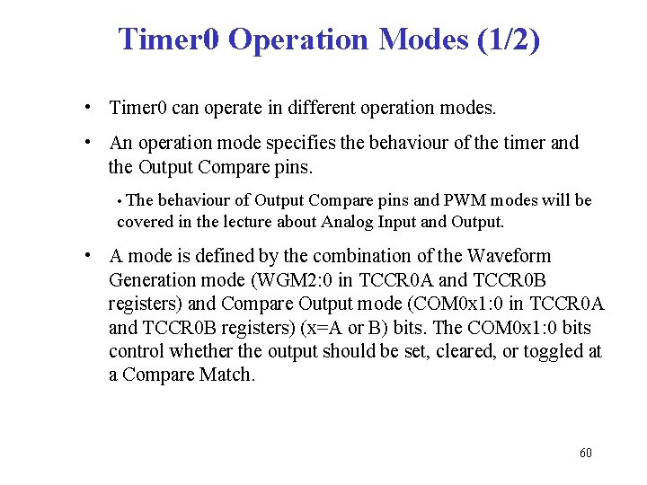
Timer 0 Operation Modes (1/2) • Timer 0 can operate in different operation modes. • An operation mode specifies the behaviour of the timer and the Output Compare pins. • The behaviour of Output Compare pins and PWM modes will be covered in the lecture about Analog Input and Output. • A mode is defined by the combination of the Waveform Generation mode (WGM 2: 0 in TCCR 0 A and TCCR 0 B registers) and Compare Output mode (COM 0 x 1: 0 in TCCR 0 A and TCCR 0 B registers) (x=A or B) bits. The COM 0 x 1: 0 bits control whether the output should be set, cleared, or toggled at a Compare Match. 60

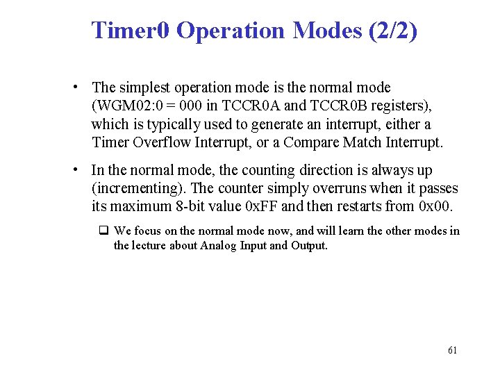
Timer 0 Operation Modes (2/2) • The simplest operation mode is the normal mode (WGM 02: 0 = 000 in TCCR 0 A and TCCR 0 B registers), which is typically used to generate an interrupt, either a Timer Overflow Interrupt, or a Compare Match Interrupt. • In the normal mode, the counting direction is always up (incrementing). The counter simply overruns when it passes its maximum 8 -bit value 0 x. FF and then restarts from 0 x 00. q We focus on the normal mode now, and will learn the other modes in the lecture about Analog Input and Output. 61

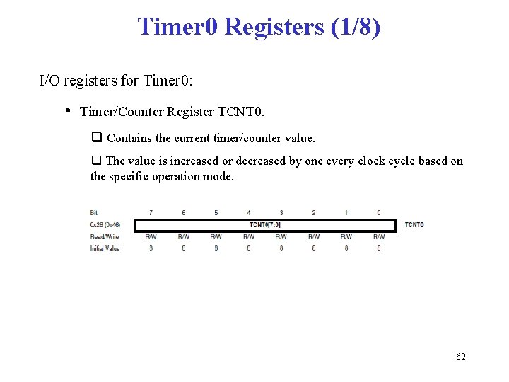
Timer 0 Registers (1/8) I/O registers for Timer 0: • Timer/Counter Register TCNT 0. q Contains the current timer/counter value. q The value is increased or decreased by one every clock cycle based on the specific operation mode. 62

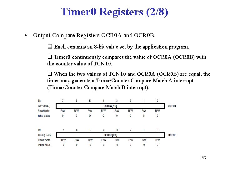
Timer 0 Registers (2/8) • Output Compare Registers OCR 0 A and OCR 0 B. q Each contains an 8 -bit value set by the application program. q Timer 0 continuously compares the value of OCR 0 A (OCR 0 B) with the counter value of TCNT 0. q When the two values of TCNT 0 and OCR 0 A (OCR 0 B) are equal, the timer may generate a Timer/Counter Compare Match A interrupt (Timer/Counter Compare Match B interrupt). 63

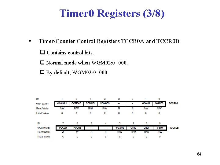
Timer 0 Registers (3/8) • Timer/Counter Control Registers TCCR 0 A and TCCR 0 B. q Contains control bits. q Normal mode when WGM 02: 0=000. q By default, WGM 02: 0=000. 64

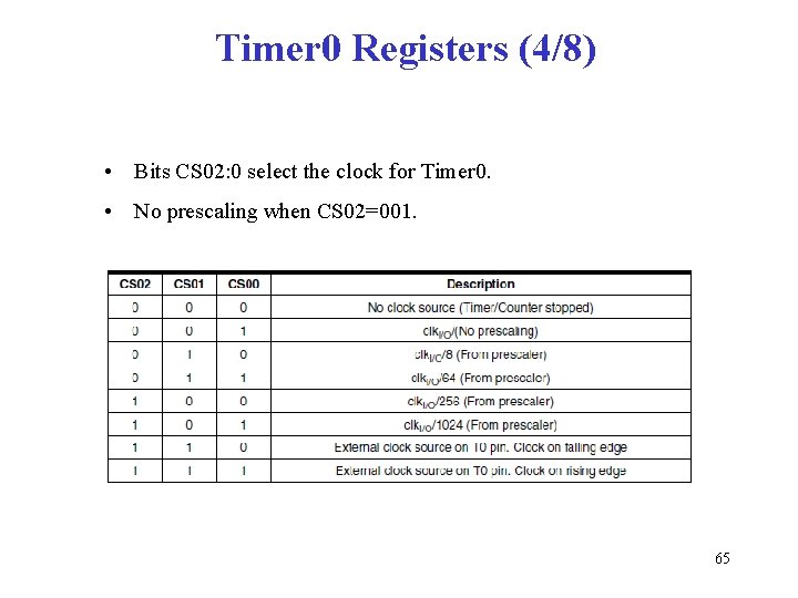
Timer 0 Registers (4/8) • Bits CS 02: 0 select the clock for Timer 0. • No prescaling when CS 02=001. 65

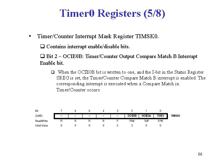
Timer 0 Registers (5/8) • Timer/Counter Interrupt Mask Register TIMSK 0. q Contains interrupt enable/disable bits. q Bit 2 – OCIE 0 B: Timer/Counter Output Compare Match B Interrupt Enable bit. q When the OCIE 0 B bit is written to one, and the I-bit in the Status Register SREG is set, the Timer/Counter Compare Match B interrupt is enabled. The corresponding interrupt is executed when a Compare Match in Timer/Counter occurs. 66

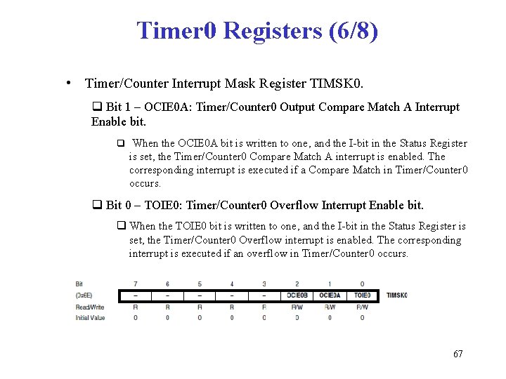
Timer 0 Registers (6/8) • Timer/Counter Interrupt Mask Register TIMSK 0. q Bit 1 – OCIE 0 A: Timer/Counter 0 Output Compare Match A Interrupt Enable bit. q When the OCIE 0 A bit is written to one, and the I-bit in the Status Register is set, the Timer/Counter 0 Compare Match A interrupt is enabled. The corresponding interrupt is executed if a Compare Match in Timer/Counter 0 occurs. q Bit 0 – TOIE 0: Timer/Counter 0 Overflow Interrupt Enable bit. q When the TOIE 0 bit is written to one, and the I-bit in the Status Register is set, the Timer/Counter 0 Overflow interrupt is enabled. The corresponding interrupt is executed if an overflow in Timer/Counter 0 occurs. 67

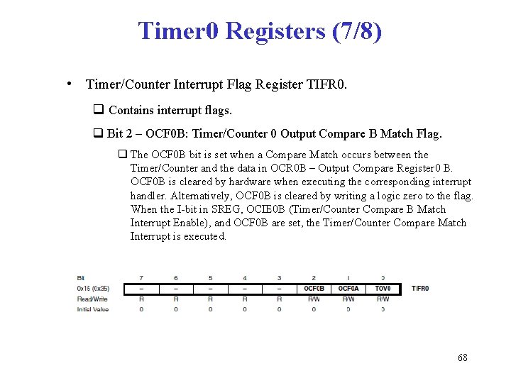
Timer 0 Registers (7/8) • Timer/Counter Interrupt Flag Register TIFR 0. q Contains interrupt flags. q Bit 2 – OCF 0 B: Timer/Counter 0 Output Compare B Match Flag. q The OCF 0 B bit is set when a Compare Match occurs between the Timer/Counter and the data in OCR 0 B – Output Compare Register 0 B. OCF 0 B is cleared by hardware when executing the corresponding interrupt handler. Alternatively, OCF 0 B is cleared by writing a logic zero to the flag. When the I-bit in SREG, OCIE 0 B (Timer/Counter Compare B Match Interrupt Enable), and OCF 0 B are set, the Timer/Counter Compare Match Interrupt is executed. 68

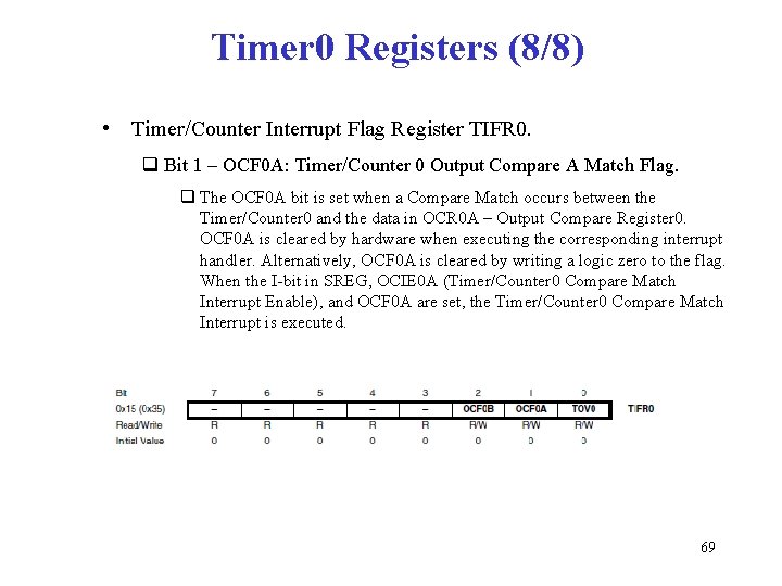
Timer 0 Registers (8/8) • Timer/Counter Interrupt Flag Register TIFR 0. q Bit 1 – OCF 0 A: Timer/Counter 0 Output Compare A Match Flag. q The OCF 0 A bit is set when a Compare Match occurs between the Timer/Counter 0 and the data in OCR 0 A – Output Compare Register 0. OCF 0 A is cleared by hardware when executing the corresponding interrupt handler. Alternatively, OCF 0 A is cleared by writing a logic zero to the flag. When the I-bit in SREG, OCIE 0 A (Timer/Counter 0 Compare Match Interrupt Enable), and OCF 0 A are set, the Timer/Counter 0 Compare Match Interrupt is executed. 69

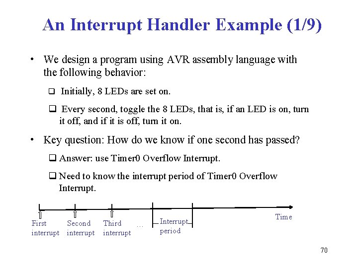
An Interrupt Handler Example (1/9) • We design a program using AVR assembly language with the following behavior: q Initially, 8 LEDs are set on. q Every second, toggle the 8 LEDs, that is, if an LED is on, turn it off, and if it is off, turn it on. • Key question: How do we know if one second has passed? q Answer: use Timer 0 Overflow Interrupt. q Need to know the interrupt period of Timer 0 Overflow Interrupt. First Second interrupt Third … interrupt Interrupt period Time 70

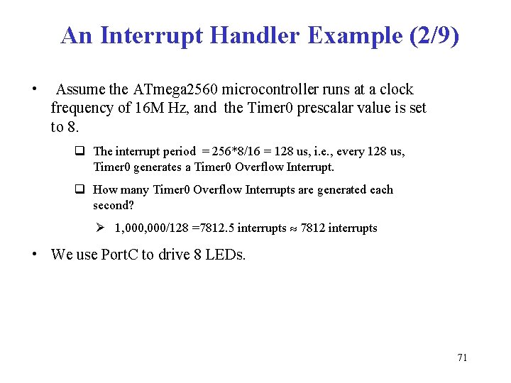
An Interrupt Handler Example (2/9) • Assume the ATmega 2560 microcontroller runs at a clock frequency of 16 M Hz, and the Timer 0 prescalar value is set to 8. q The interrupt period = 256*8/16 = 128 us, i. e. , every 128 us, Timer 0 generates a Timer 0 Overflow Interrupt. q How many Timer 0 Overflow Interrupts are generated each second? Ø 1, 000/128 =7812. 5 interrupts 7812 interrupts • We use Port. C to drive 8 LEDs. 71

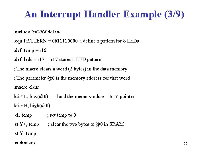
An Interrupt Handler Example (3/9). include "m 2560 def. inc". equ PATTERN = 0 b 11110000 ; define a pattern for 8 LEDs. def temp = r 16. def leds = r 17 ; r 17 stores a LED pattern ; The macro clears a word (2 bytes) in the data memory ; The parameter @0 is the memory address for that word. macro clear ldi YL, low(@0) ; load the memory address to Y pointer ldi YH, high(@0) clr temp ; set temp to 0 st Y+, temp ; clear the two bytes at @0 in SRAM st Y, temp. endmacro 72

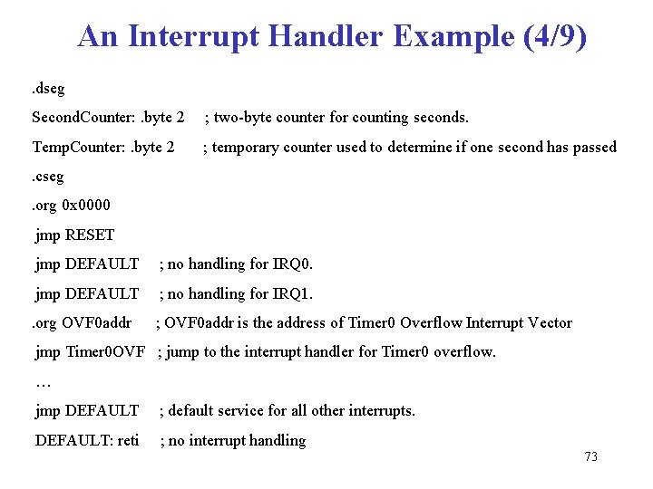
An Interrupt Handler Example (4/9). dseg Second. Counter: . byte 2 ; two-byte counter for counting seconds. Temp. Counter: . byte 2 ; temporary counter used to determine if one second has passed . cseg. org 0 x 0000 jmp RESET jmp DEFAULT ; no handling for IRQ 0. jmp DEFAULT ; no handling for IRQ 1. . org OVF 0 addr ; OVF 0 addr is the address of Timer 0 Overflow Interrupt Vector jmp Timer 0 OVF ; jump to the interrupt handler for Timer 0 overflow. … jmp DEFAULT ; default service for all other interrupts. DEFAULT: reti ; no interrupt handling 73

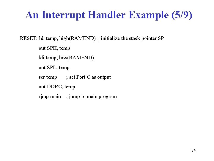
An Interrupt Handler Example (5/9) RESET: ldi temp, high(RAMEND) ; initialize the stack pointer SP out SPH, temp ldi temp, low(RAMEND) out SPL, temp ser temp ; set Port C as output out DDRC, temp rjmp main ; jump to main program 74

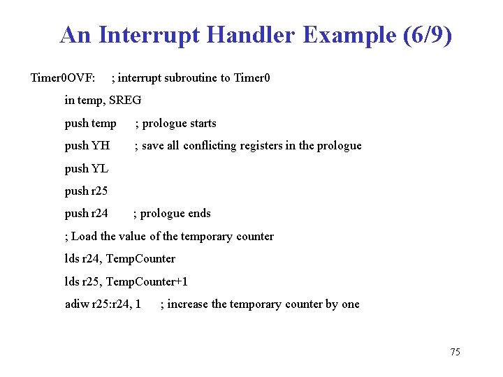
An Interrupt Handler Example (6/9) Timer 0 OVF: ; interrupt subroutine to Timer 0 in temp, SREG push temp ; prologue starts push YH ; save all conflicting registers in the prologue push YL push r 25 push r 24 ; prologue ends ; Load the value of the temporary counter lds r 24, Temp. Counter lds r 25, Temp. Counter+1 adiw r 25: r 24, 1 ; increase the temporary counter by one 75

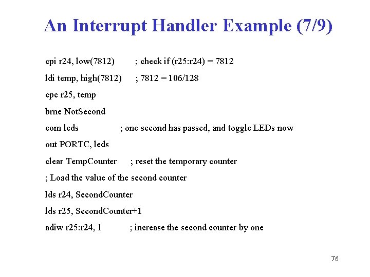
An Interrupt Handler Example (7/9) cpi r 24, low(7812) ; check if (r 25: r 24) = 7812 ldi temp, high(7812) ; 7812 = 106/128 cpc r 25, temp brne Not. Second com leds ; one second has passed, and toggle LEDs now out PORTC, leds clear Temp. Counter ; reset the temporary counter ; Load the value of the second counter lds r 24, Second. Counter lds r 25, Second. Counter+1 adiw r 25: r 24, 1 ; increase the second counter by one 76

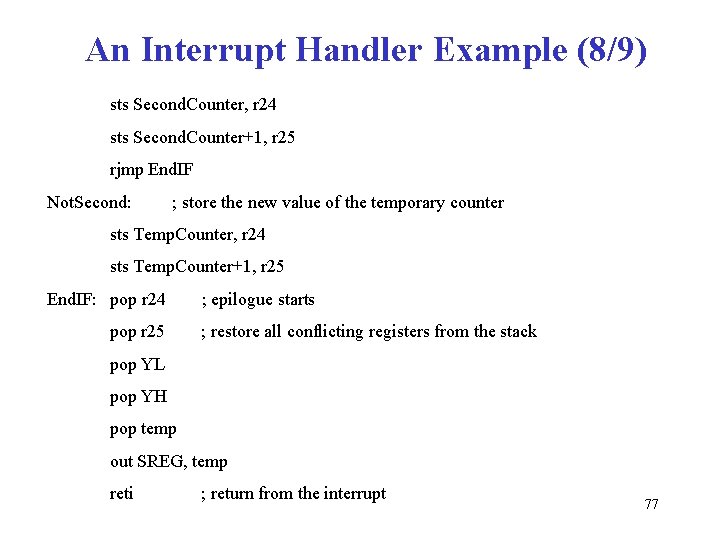
An Interrupt Handler Example (8/9) sts Second. Counter, r 24 sts Second. Counter+1, r 25 rjmp End. IF Not. Second: ; store the new value of the temporary counter sts Temp. Counter, r 24 sts Temp. Counter+1, r 25 End. IF: pop r 24 pop r 25 ; epilogue starts ; restore all conflicting registers from the stack pop YL pop YH pop temp out SREG, temp reti ; return from the interrupt 77

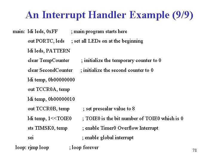
An Interrupt Handler Example (9/9) main: ldi leds, 0 x. FF ; main program starts here out PORTC, leds ; set all LEDs on at the beginning ldi leds, PATTERN clear Temp. Counter ; initialize the temporary counter to 0 clear Second. Counter ; initialize the second counter to 0 ldi temp, 0 b 0000 out TCCR 0 A, temp ldi temp, 0 b 00000010 out TCCR 0 B, temp ; set prescalar value to 8 ldi temp, 1<<TOIE 0 ; TOIE 0 is the bit number of TOIE 0 which is 0 sts TIMSK 0, temp ; enable Timer 0 Overflow Interrupt sei ; enable global interrupt loop: rjmp loop ; loop forever 78

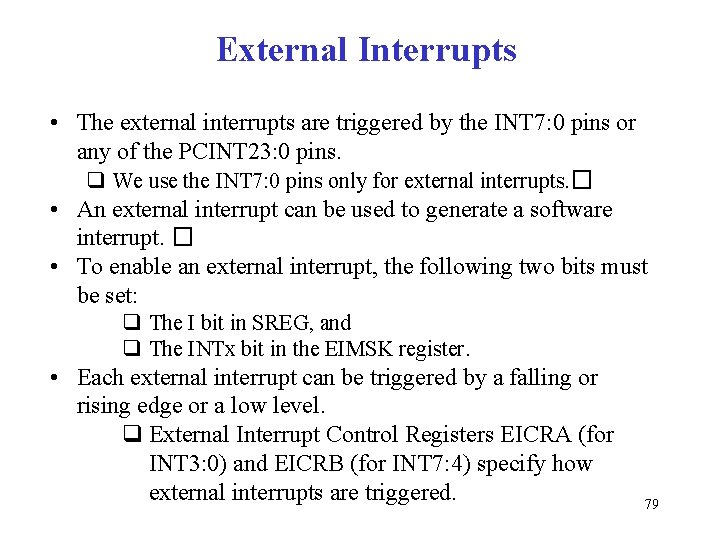
External Interrupts • The external interrupts are triggered by the INT 7: 0 pins or any of the PCINT 23: 0 pins. q We use the INT 7: 0 pins only for external interrupts. � • An external interrupt can be used to generate a software interrupt. � • To enable an external interrupt, the following two bits must be set: q The I bit in SREG, and q The INTx bit in the EIMSK register. • Each external interrupt can be triggered by a falling or rising edge or a low level. q External Interrupt Control Registers EICRA (for INT 3: 0) and EICRB (for INT 7: 4) specify how external interrupts are triggered. 79

Registers for External Interrupts (1/4) • EICRA – External Interrupt Control Register A q EICRA contains bits for interrupt sense control (INT 3: 0). � 80

Registers for External Interrupts (2/4) • EICRB – External Interrupt Control Register B q EICRB contains bits for interrupt sense control (INT 7: 4). � 81

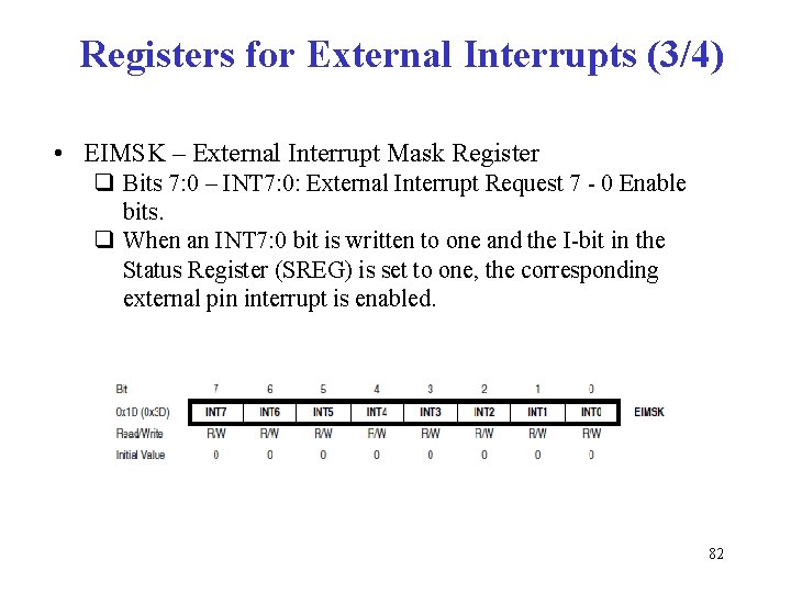
Registers for External Interrupts (3/4) • EIMSK – External Interrupt Mask Register q Bits 7: 0 – INT 7: 0: External Interrupt Request 7 - 0 Enable bits. q When an INT 7: 0 bit is written to one and the I-bit in the Status Register (SREG) is set to one, the corresponding external pin interrupt is enabled. 82

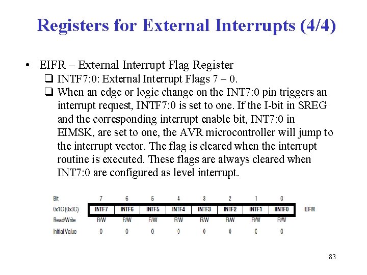
Registers for External Interrupts (4/4) • EIFR – External Interrupt Flag Register q INTF 7: 0: External Interrupt Flags 7 – 0. q When an edge or logic change on the INT 7: 0 pin triggers an interrupt request, INTF 7: 0 is set to one. If the I-bit in SREG and the corresponding interrupt enable bit, INT 7: 0 in EIMSK, are set to one, the AVR microcontroller will jump to the interrupt vector. The flag is cleared when the interrupt routine is executed. These flags are always cleared when INT 7: 0 are configured as level interrupt. 83

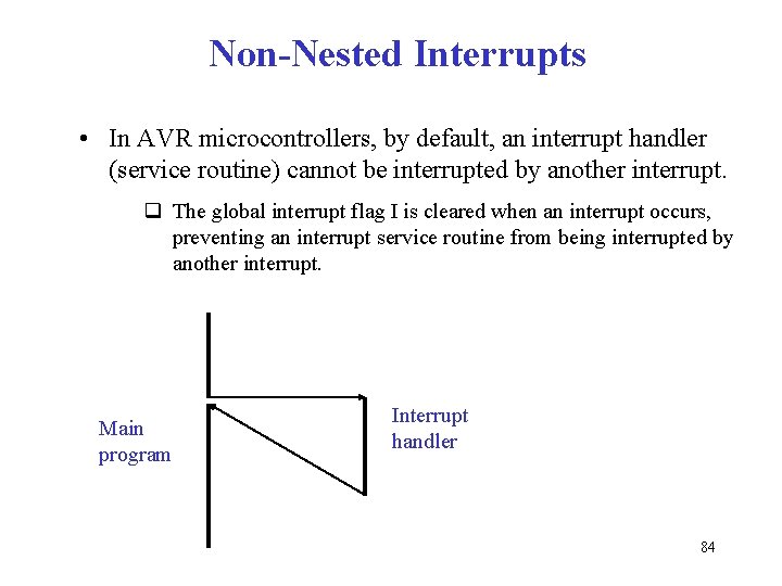
Non-Nested Interrupts • In AVR microcontrollers, by default, an interrupt handler (service routine) cannot be interrupted by another interrupt. q The global interrupt flag I is cleared when an interrupt occurs, preventing an interrupt service routine from being interrupted by another interrupt. Main program Interrupt handler 84

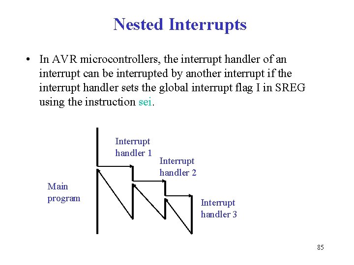
Nested Interrupts • In AVR microcontrollers, the interrupt handler of an interrupt can be interrupted by another interrupt if the interrupt handler sets the global interrupt flag I in SREG using the instruction sei. Interrupt handler 1 Main program Interrupt handler 2 Interrupt handler 3 85

Reading Material 1. Chapter 8. Microcontrollers and Microcomputers. 2. Read the following sections in ATmega 2560 Data Sheet: a. Overview b. System Control and Reset. c. Watchdog Timer. d. Interrupts. e. External Interrupts. f. 8 -bit Time/Counter 0 86