COMP 211 Computer Logic Design Lecture 6 Memory


- Slides: 30

COMP 211 Computer Logic Design Lecture 6. Memory Prof. Taeweon Suh Computer Science Education Korea University

Memory • Digital systems including computer systems require memories § Memory is used to store instructions and data • Registers (made from flip-flops) are kind of memory § But, how many transistors need to build a 1 -bit register (that is, to store 1 -bit) with a flip-flop? • Here we study memory arrays that can efficiently store large amounts of data § RAM and ROM 2 Korea Univ

Memory • Random Access Memory (RAM) § Static Random Access Memory (SRAM) • • Data stored so long as power is applied 6 -transistors per cell Faster Differential § Dynamic Random Access Memory (DRAM) • • Require periodic refresh Smaller (can be implemented with 1 or 3 transistors) Slower Single-Ended § Can be read and written • Read-Only Memory (ROM) Modified from Prof Sean Lee’s Slide, Georgia Tech 3 Korea Univ

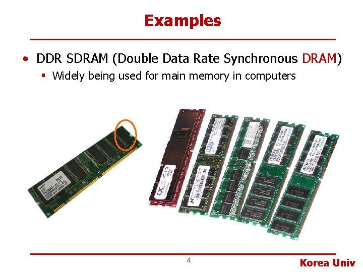
Examples • DDR SDRAM (Double Data Rate Synchronous DRAM) § Widely being used for main memory in computers 4 Korea Univ

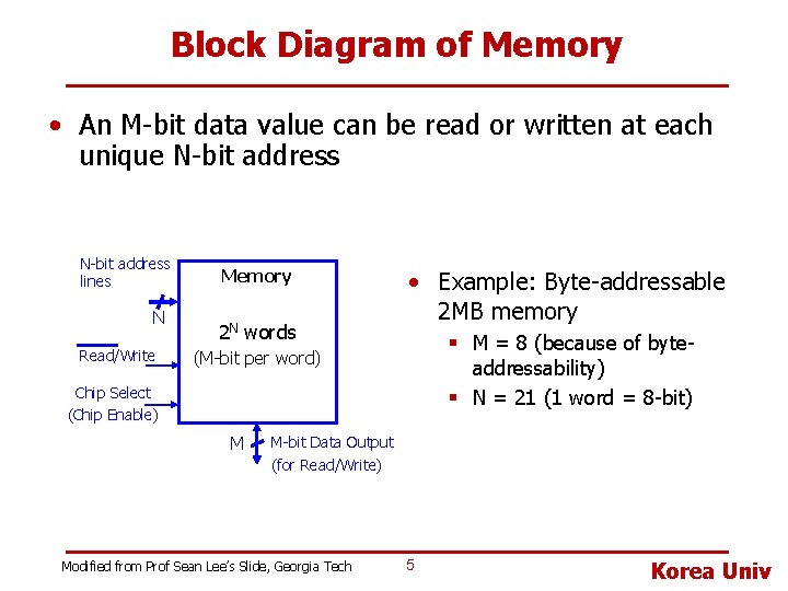
Block Diagram of Memory • An M-bit data value can be read or written at each unique N-bit address lines N Read/Write Memory 2 N words • Example: Byte-addressable 2 MB memory § M = 8 (because of byteaddressability) § N = 21 (1 word = 8 -bit) (M-bit per word) Chip Select (Chip Enable) M M-bit Data Output (for Read/Write) Modified from Prof Sean Lee’s Slide, Georgia Tech 5 Korea Univ

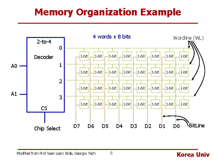
Memory Organization Example 2 -to-4 4 words x 8 bits Wordline (WL) 0 Decoder 1 -bit 1 -bit 1 -bit 1 -bit 1 -bit 1 -bit 1 -bit 1 -bit 1 A 0 2 A 1 3 CS Chip Select D 7 D 6 Modified from Prof Sean Lee’s Slide, Georgia Tech D 4 D 5 6 D 3 D 2 D 1 D 0 Bit. Line Korea Univ

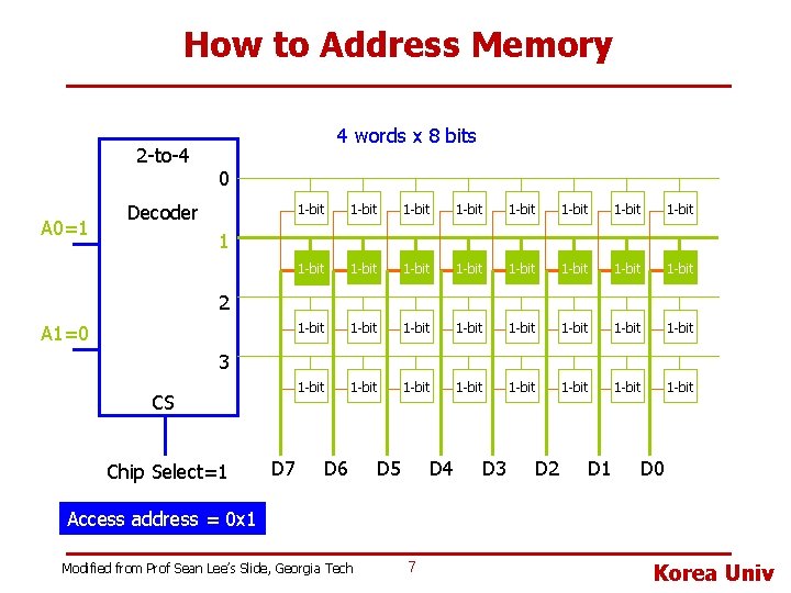
How to Address Memory 2 -to-4 A 0=1 4 words x 8 bits 0 Decoder 1 -bit 1 -bit 1 -bit 1 -bit 1 -bit 1 -bit 1 -bit 1 -bit 1 2 A 1=0 3 CS Chip Select=1 D 7 D 6 D 4 D 5 D 3 D 2 D 1 D 0 Access address = 0 x 1 Modified from Prof Sean Lee’s Slide, Georgia Tech 7 Korea Univ

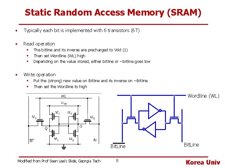
Static Random Access Memory (SRAM) • Typically each bit is implemented with 6 transistors (6 T) • Read operation § § § • The bitline and its inverse are precharged to Vdd (1) Then set Wordline (WL) high Depending on the value stored, either bitline or ~bitline goes low Write operation § § Put the (strong) new value on Bitline and its inverse on ~Bitline Then set the Wordline to high Wordline (WL) Bit. Line Modified from Prof Sean Lee’s Slide, Georgia Tech 8 Bit. Line Korea Univ

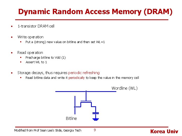
Dynamic Random Access Memory (DRAM) • 1 -transistor DRAM cell • Write operation § • Read operation § § • Put a (strong) new value on bitline and then set WL=1 Precharge bitline to Vdd (1) Assert WL to 1 Storage decays, thus requires periodic refreshing § Read bitline data and write it periodically to keep the value in the memory cell Wordline (WL) Bitline Modified from Prof Sean Lee’s Slide, Georgia Tech 9 Korea Univ

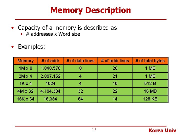
Memory Description • Capacity of a memory is described as § # addresses x Word size • Examples: Memory # of addr # of data lines # of addr lines # of total bytes 1 M x 8 1, 048, 576 8 20 1 MB 2 M x 4 2, 097, 152 4 21 1 MB 1 K x 4 1024 4 10 512 B 4 M x 32 4, 194, 304 32 22 16 MB 16 K x 64 16, 384 64 14 128 KB 10 Korea Univ

Example 11 Korea Univ

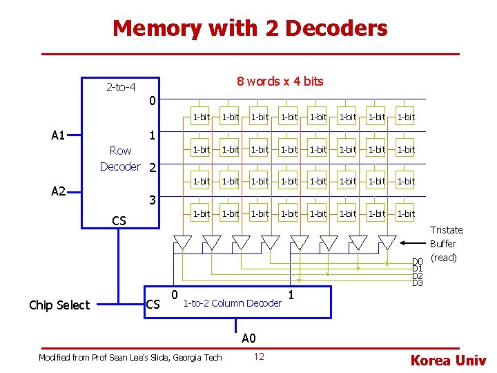
Memory with 2 Decoders 2 -to-4 8 words x 4 bits 0 1 -bit 1 -bit 1 -bit 1 -bit 1 -bit 1 -bit 1 -bit 1 -bit 1 A 1 Row Decoder 2 A 2 3 CS Chip Select 1 -bit Tristate Buffer D 0 (read) CS 0 1 -to-2 Column Decoder 1 D 2 D 3 A 0 Modified from Prof Sean Lee’s Slide, Georgia Tech 12 Korea Univ

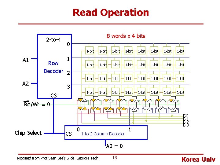
Read Operation 2 -to-4 A 1 8 words x 4 bits 0 1 -bit 1 -bit 1 -bit 1 -bit 1 -bit 1 -bit 1 -bit 1 -bit 1 Row Decoder 2 A 2 3 CS Rd/Wr = 0 Chip Select CS 0 1 -to-2 Column Decoder 1 D 0 D 1 D 2 D 3 A 0 = 0 Modified from Prof Sean Lee’s Slide, Georgia Tech 13 Korea Univ

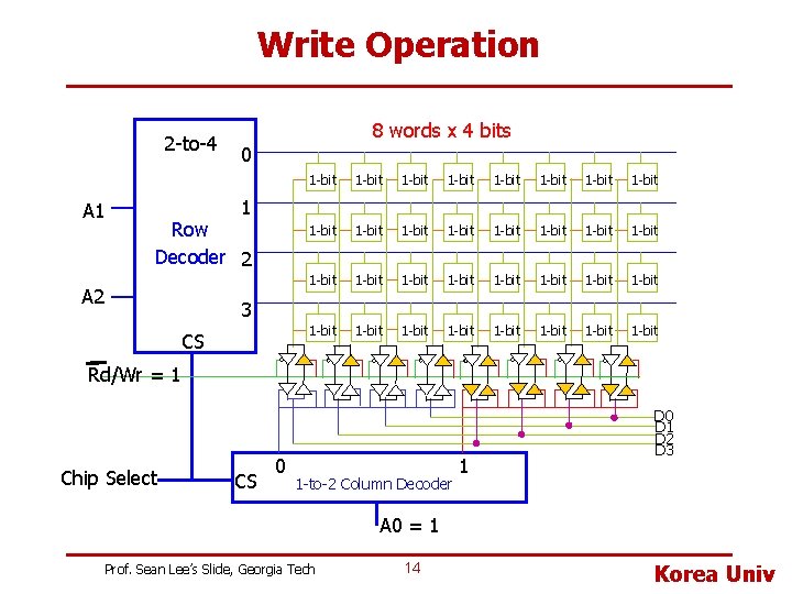
Write Operation 2 -to-4 A 1 8 words x 4 bits 0 1 -bit 1 -bit 1 -bit 1 -bit 1 -bit 1 -bit 1 -bit 1 -bit 1 Row Decoder 2 A 2 3 CS Rd/Wr = 1 Chip Select CS 0 1 -to-2 Column Decoder 1 D 0 D 1 D 2 D 3 A 0 = 1 Prof. Sean Lee’s Slide, Georgia Tech 14 Korea Univ

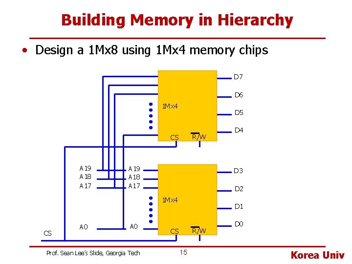
Building Memory in Hierarchy • Design a 1 Mx 8 using 1 Mx 4 memory chips D 7 D 6 1 Mx 4 D 5 R/W CS A 19 A 18 A 17 D 3 D 2 1 Mx 4 CS A 0 Prof. Sean Lee’s Slide, Georgia Tech D 4 D 1 R/W CS 15 D 0 Korea Univ

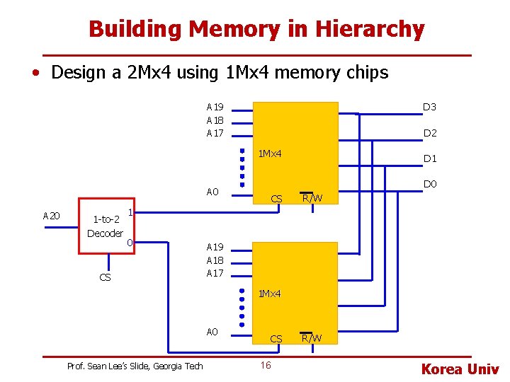
Building Memory in Hierarchy • Design a 2 Mx 4 using 1 Mx 4 memory chips A 19 A 18 A 17 D 3 D 2 1 Mx 4 D 0 A 20 1 -to-2 Decoder D 1 CS R/W 1 0 CS A 19 A 18 A 17 1 Mx 4 A 0 Prof. Sean Lee’s Slide, Georgia Tech CS 16 R/W Korea Univ

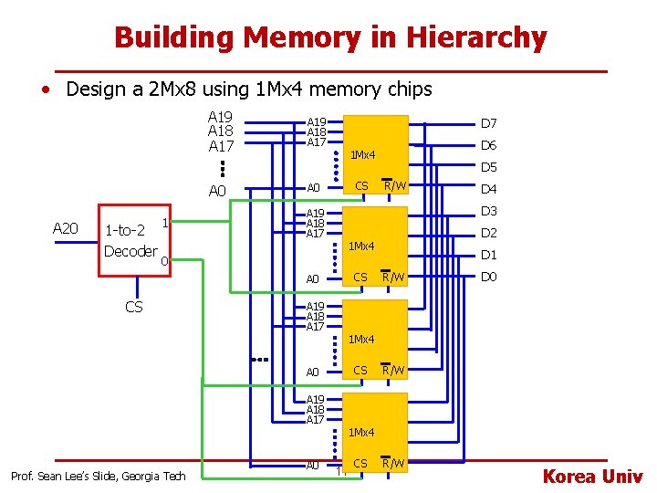
Building Memory in Hierarchy • Design a 2 Mx 8 using 1 Mx 4 memory chips A 19 A 18 A 17 A 0 A 20 1 -to-2 Decoder 1 D 7 A 19 A 18 A 17 CS A 0 A 19 A 18 A 17 Prof. Sean Lee’s Slide, Georgia Tech A 0 R/W D 4 D 2 1 Mx 4 CS D 1 R/W D 0 1 Mx 4 CS A 0 A 19 A 18 A 17 D 5 D 3 A 0 CS D 6 1 Mx 4 R/W 1 Mx 4 17 CS R/W Korea Univ

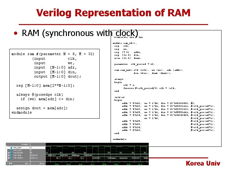
Verilog Representation of RAM • RAM (synchronous with clock) `timescale 1 ns / 1 ns module ram #(parameter N (input [N-1: 0] input [M-1: 0] output [M-1: 0] = 8, M = 32) clk, we, adr, din, dout); reg [M-1: 0] mem[2**N-1: 0]; always @(posedge clk) if (we) mem[adr] <= din; assign dout = mem[adr]; endmodule ram_tb(); reg clk; reg we; reg [7: 0] addr; reg [31: 0] din; wire [31: 0] dout; parameter clk_period = 10; ram_uut(. clk (clk), . we (we), . adr (addr), . din (din), . dout (dout)); always begin clk = 1; forever #(clk_period/2) clk = ~clk; end initial begin addr addr = = = 4'h 00; 4'h 02; 4'h 09; 4'h 34; addr = = 4'h 09; 4'h 02; 4'h 34; 4'h 00; we we we = = = 1'b 0; 1'b 1; 1'b 0; din din din = = = 32'h 0000; 32'h 00001111; 32'h 22223333; 32'h 9999 AAAA; 32'h 3434; #3; #(clk_period*1); #(clk_period*1); #(clk_period*1); endmodule 18 Korea Univ

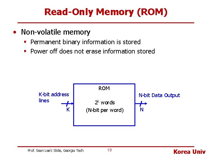
Read-Only Memory (ROM) • Non-volatile memory § Permanent binary information is stored § Power off does not erase information stored K-bit address lines K Prof. Sean Lee’s Slide, Georgia Tech ROM N-bit Data Output 2 k words (N-bit per word) 19 N Korea Univ

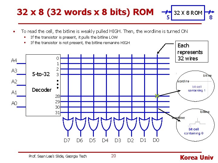
32 x 8 (32 words x 8 bits) ROM • 8 To read the cell, the bitline is weakly pulled HIGH. Then, the wordline is turned ON § § If the transistor is present, it pulls the bitline LOW If the transistor is not present, the bitline remanins HIGH A 4 A 3 5 32 X 8 ROM 5 -to-32 Each represents 32 wires 0 1 2 3 A 2 A 1 A 0 Decoder 28 29 30 31 D 7 D 6 Prof. Sean Lee’s Slide, Georgia Tech D 5 D 4 D 3 20 D 2 D 1 D 0 Korea Univ

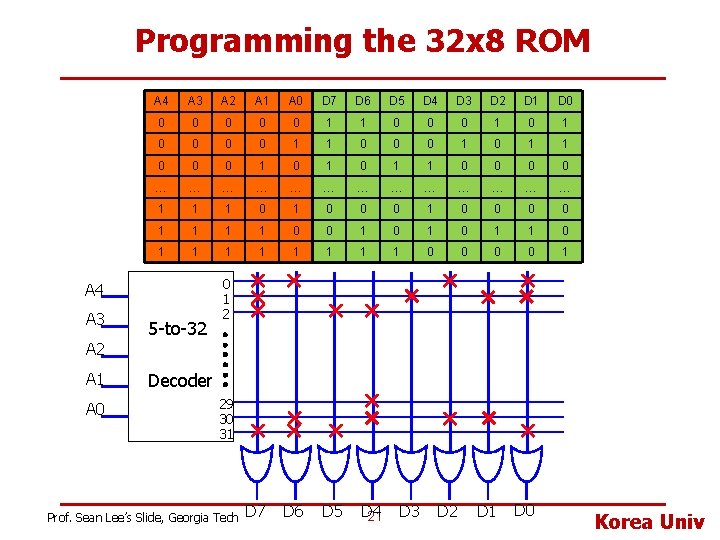
Programming the 32 x 8 ROM A 4 A 3 A 2 A 1 A 0 D 7 D 6 D 5 D 4 D 3 D 2 D 1 D 0 0 0 1 1 0 0 0 1 0 1 0 1 1 0 0 … … … … 1 1 1 0 0 0 1 1 0 0 1 0 1 1 1 1 1 0 0 1 D 6 D 5 D 4 21 A 4 A 3 A 2 A 1 A 0 5 -to-32 0 1 2 Decoder 29 30 31 Prof. Sean Lee’s Slide, Georgia Tech D 7 D 3 D 2 D 1 D 0 Korea Univ

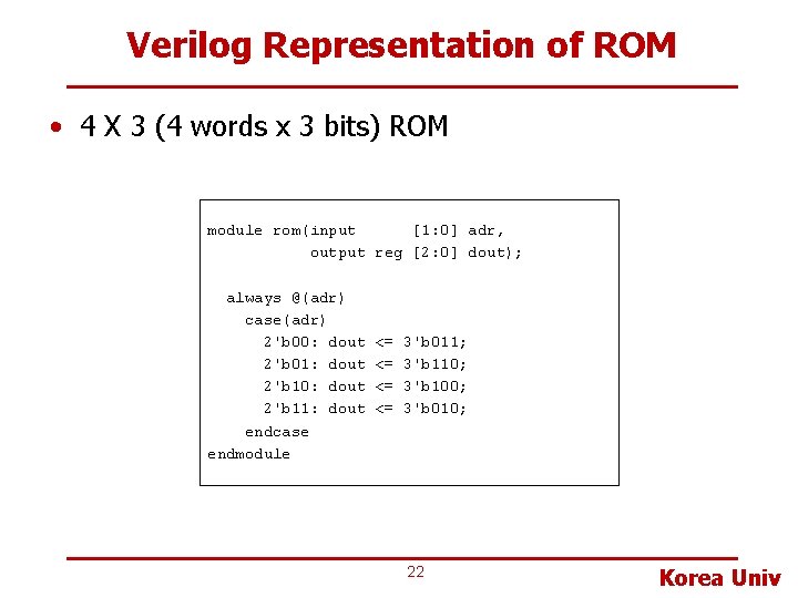
Verilog Representation of ROM • 4 X 3 (4 words x 3 bits) ROM module rom(input [1: 0] adr, output reg [2: 0] dout); always @(adr) case(adr) 2'b 00: dout 2'b 01: dout 2'b 10: dout 2'b 11: dout endcase endmodule <= <= 3'b 011; 3'b 110; 3'b 100; 3'b 010; 22 Korea Univ

Other Flavors of ROMs • Reprogrammable ROMs § EPROM (Erasable Programmable ROM) • Use UV (Ultra Violet) light for erasing § EEPROM (Electrically Erasable Programmable ROM) • Flash memory § Read and Writable § Non-volatile • Power off does not erase information stored • Modern ROMs are not really read-only § They can be reprogrammed as well • Flash memory has become extremely popular to store large amounts of data in portable systems such as cameras and music players 23 Korea Univ

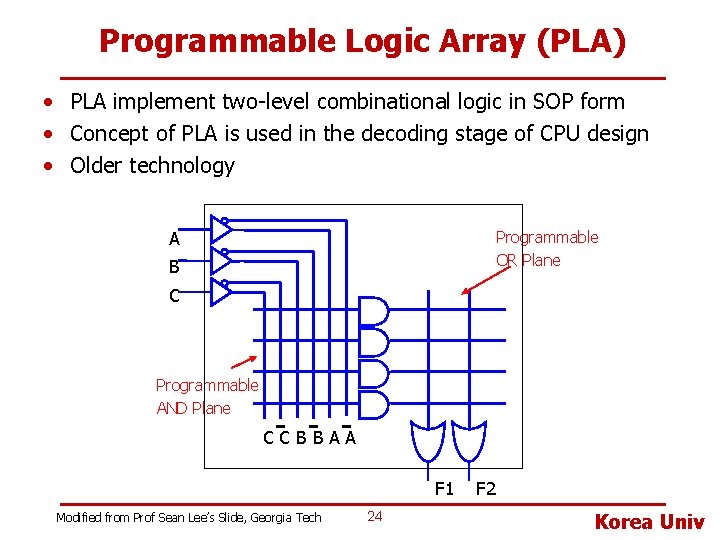
Programmable Logic Array (PLA) • PLA implement two-level combinational logic in SOP form • Concept of PLA is used in the decoding stage of CPU design • Older technology A Programmable OR Plane B C Programmable AND Plane CCBBAA F 1 Modified from Prof Sean Lee’s Slide, Georgia Tech 24 F 2 Korea Univ

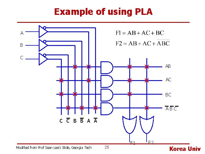
Example of using PLA A B C AB AC BC ABC C C B B A A Modified from Prof Sean Lee’s Slide, Georgia Tech 25 F 1 F 2 Korea Univ

FPGA • Field Programmable Gate Array (FPGA) can implement both combinational and sequential logic § PLA can implement only combinational logic • Using CAD tools, a user can implement designs on the FPGA using either HDL or schematic • It is programmable in the field § FPGA is reprogrammable (reconfigurable) after a system is deployed • 2 Major FPGA companies § Xilinx: www. xilinx. com § Altera: www. altera. com 26 Korea Univ

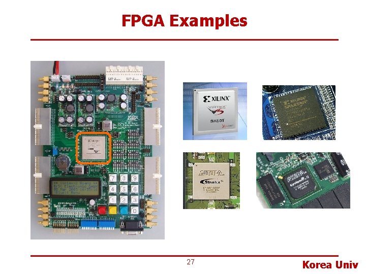
FPGA Examples 27 Korea Univ

The End • That’s it! Folks • I hope you have enjoyed this class • You just got one step closer to understanding computers • See you next semester in the computer architecture class 28 Korea Univ

Backup Slides 29 Korea Univ

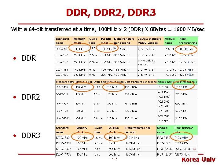
DDR, DDR 2, DDR 3 With a 64 -bit transferred at a time, 100 MHz x 2 (DDR) X 8 Bytes = 1600 MB/sec • DDR 2 • DDR 3 30 Korea Univ