Common source output stage Vxx When Vo 1

- Slides: 23

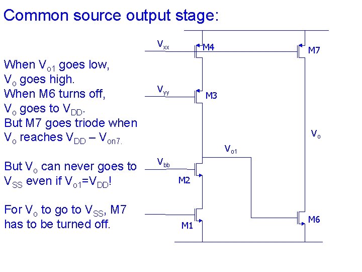
Common source output stage: Vxx When Vo 1 goes low, Vo goes high. When M 6 turns off, Vo goes to VDD. But M 7 goes triode when Vo reaches VDD – Von 7. But Vo can never goes to VSS even if Vo 1=VDD! For Vo to go to VSS, M 7 has to be turned off. M 4 Vyy M 7 M 3 Vo Vo 1 Vbb M 2 M 1 M 6

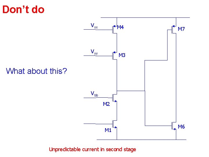
Don’t do Vxx M 4 Vyy M 7 M 3 What about this? Vbb M 2 M 1 Unpredictable current in second stage M 6

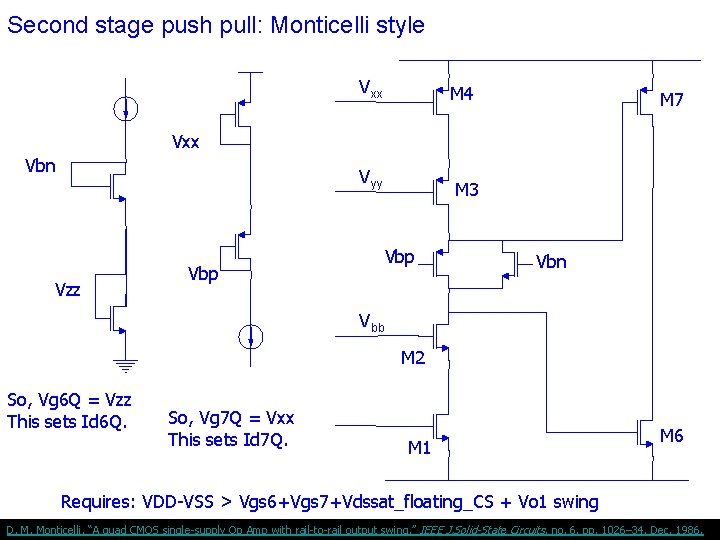
Second stage push pull: Monticelli style Vxx M 4 M 7 Vxx Vbn Vyy Vzz Vbp M 3 Vbp Vbn Vbb M 2 So, Vg 6 Q = Vzz This sets Id 6 Q. So, Vg 7 Q = Vxx This sets Id 7 Q. M 1 M 6 Requires: VDD-VSS > Vgs 6+Vgs 7+Vdssat_floating_CS + Vo 1 swing D. M. Monticelli, “A quad CMOS single-supply Op Amp with rail-to-rail output swing, ” IEEE J. Solid-State Circuits, no. 6, pp. 1026– 34, Dec. 1986.

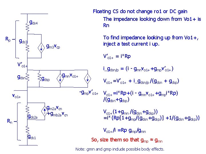
Floating CS do not change ro 1 or DC gain The impedance looking down from Vo 1+ is Rn gds 4 Rp gds 3 To find impedance looking up from Vo 1+, inject a test current i up. gm 3 vcp V’o 1+ = i*Rp V’o 1+ gdsn gdsp gmnvo 1+ Vo 1+=V’o 1+ + i_gdsn/p /(gdsn + gdsp) -gmpv’o 1+ V =i*Rp+(i - g v +g i*Rp) o 1+ mn o 1+ mp /(gdsn+gdsp) vo 1+ Rn i_gdsn/p = (i - gmnvo 1++gmpv’o 1+) gds 2 a gds 1 gm 2 avcn +gmb 2 avcn Vo 1+(1+gmn /(gdsn+gdsp)) =i*{Rp[1+gmp/(gdsn+gdsp)] +1/(gdsn+gdsp)} Vo 1+/i =Rp gmp/gmn So, size them so that gmp ≈ gmn Note: gmn and gmp include possible body effects.

To the two gate terminals of M 6 and M 7, the two floating CS appears as a voltage source providing a voltage offset between the gates. The impedance seen by the two gate terminals can be calculated by: Rs = (Vgp – Vgn)/(current through the floating CS) = (Vgp – Vgn)/(gmp*Vgp – gmn*Vgn + (Vgp – Vgn)*(gdsn+gdsp)) ≈ 1/(gmp + gdsn+gdsp) ≈ 1/gmp The above assumed that the NMOS and PMOS are sized to have the same gm. Also, the calculation is only valid when both NMOS and PMOS are fully on and both in saturation. When Vo is experiencing large swings, these conditions are not met. And the voltage difference between the two gate terminals no longer remain constant.

HW: summarize the above discussion into a design procedure for given desired bias currents in output stage Io and the cascade stage Ic. Suppose a Iref is given. HW: find Vo swing range, if all transistors remain in saturation. Find io range if all transistors remain in saturation, where io = i 7 – i 6. When the floating current source transistors are allowed to go into triode but all other transistors need to remain in saturation, what is the io range?

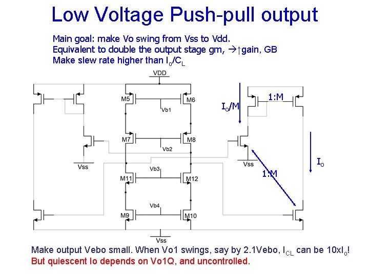
Low Voltage Push-pull output Main goal: make Vo swing from Vss to Vdd. Equivalent to double the output stage gm, ↑gain, GB Make slew rate higher than Io/CL Io/M 1: M Io Make output Vebo small. When Vo 1 swings, say by 2. 1 Vebo, ICL can be 10 x. Io! But quiescent Io depends on Vo 1 Q, and uncontrolled.

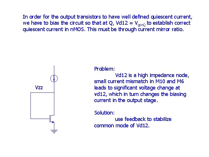
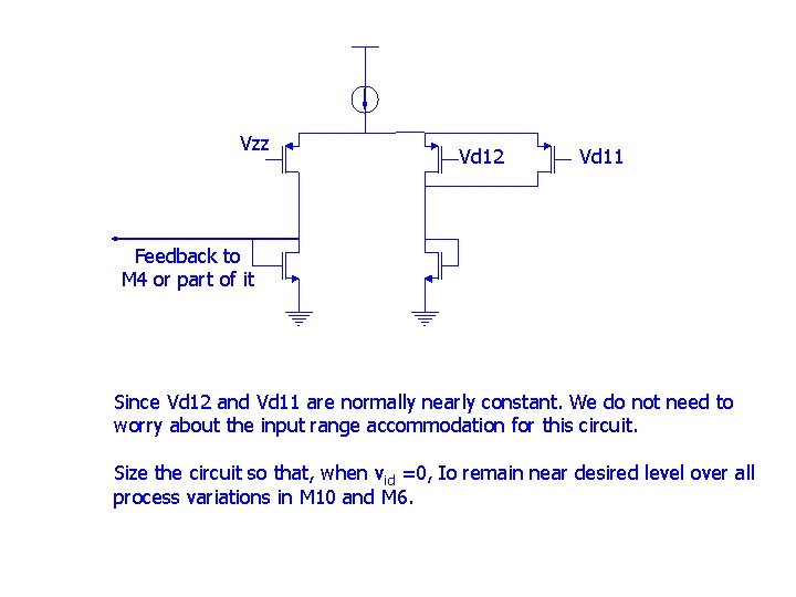
In order for the output transistors to have well defined quiescent current, we have to bias the circuit so that at Q, Vd 12 = Vgsn. Q to establish correct quiescent current in n. MOS. This must be through current mirror ratio. Problem: Vzz Vd 12 is a high impedance node, small current mismatch in M 10 and M 6 leads to significant voltage change at vd 12, which in turn changes the biasing current in the output stage. Solution: use feedback to stabilize common mode of Vd 12.

Vzz Vd 12 Vd 11 Feedback to M 4 or part of it Since Vd 12 and Vd 11 are normally nearly constant. We do not need to worry about the input range accommodation for this circuit. Size the circuit so that, when vid =0, Io remain near desired level over all process variations in M 10 and M 6.

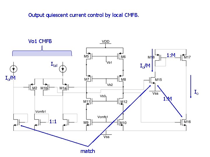
Output quiescent current control by local CMFB. Vo 1 CMFB 1: M Itail Io/M 1: 1 match Io

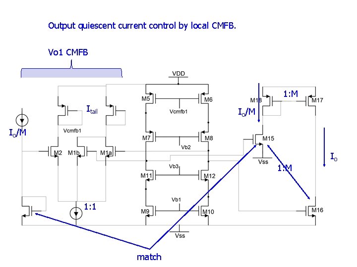
Output quiescent current control by local CMFB. Vo 1 CMFB 1: M Itail Io/M 1: 1 match Io

Can passive CM detector be use?

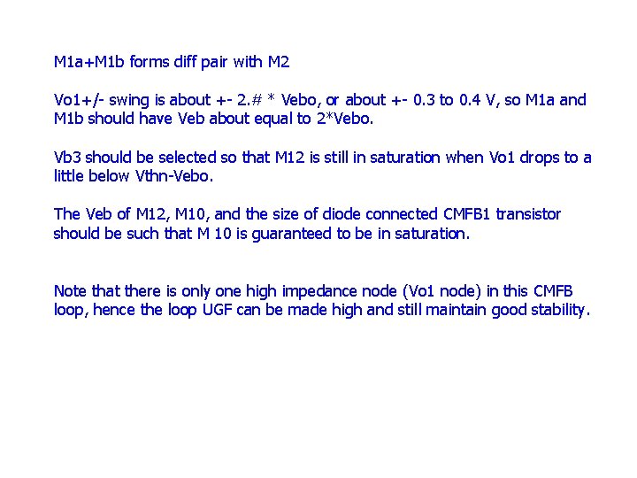
M 1 a+M 1 b forms diff pair with M 2 Vo 1+/- swing is about +- 2. # * Vebo, or about +- 0. 3 to 0. 4 V, so M 1 a and M 1 b should have Veb about equal to 2*Vebo. Vb 3 should be selected so that M 12 is still in saturation when Vo 1 drops to a little below Vthn-Vebo. The Veb of M 12, M 10, and the size of diode connected CMFB 1 transistor should be such that M 10 is guaranteed to be in saturation. Note that there is only one high impedance node (Vo 1 node) in this CMFB loop, hence the loop UGF can be made high and still maintain good stability.

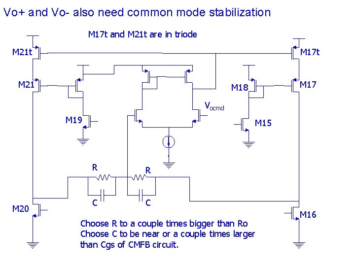
Vo+ and Vo- also need common mode stabilization M 17 t and M 21 t are in triode M 21 t M 17 t M 21 M 17 M 18 Vocmd M 19 M 20 M 15 R R C C Choose R to a couple times bigger than Ro Choose C to be near or a couple times larger than Cgs of CMFB circuit. M 16

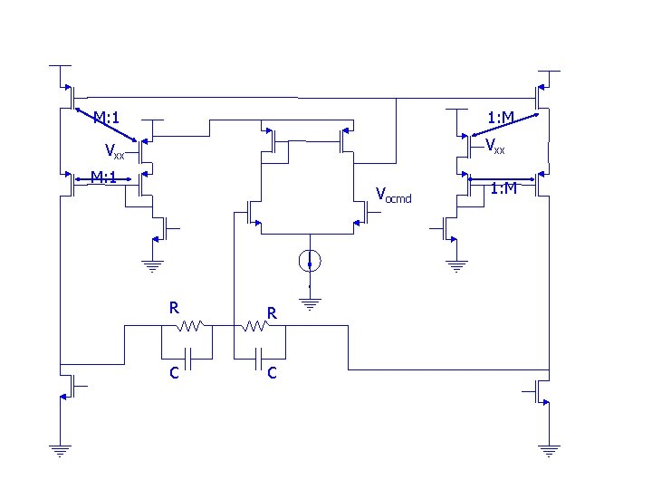
M: 1 1: M Vxx M: 1 Vocmd R R C C 1: M

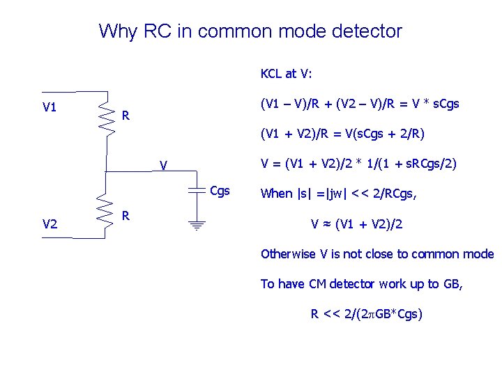
Why RC in common mode detector KCL at V: V 1 (V 1 – V)/R + (V 2 – V)/R = V * s. Cgs R (V 1 + V 2)/R = V(s. Cgs + 2/R) V = (V 1 + V 2)/2 * 1/(1 + s. RCgs/2) V Cgs V 2 R When |s| =|jw| << 2/RCgs, V ≈ (V 1 + V 2)/2 Otherwise V is not close to common mode To have CM detector work up to GB, R << 2/(2 p. GB*Cgs)

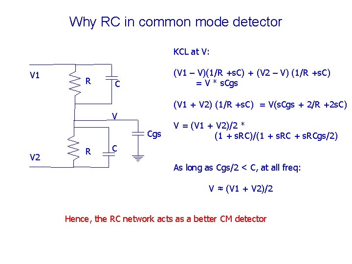
Why RC in common mode detector KCL at V: V 1 R (V 1 – V)(1/R +s. C) + (V 2 – V) (1/R +s. C) = V * s. Cgs C (V 1 + V 2) (1/R +s. C) = V(s. Cgs + 2/R +2 s. C) V Cgs V 2 R V = (V 1 + V 2)/2 * (1 + s. RC)/(1 + s. RCgs/2) C As long as Cgs/2 < C, at all freq: V ≈ (V 1 + V 2)/2 Hence, the RC network acts as a better CM detector

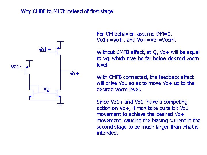
Why CMBF to M 17 t instead of first stage: For CM behavior, assume DM=0. Vo 1+=Vo 1 -, and Vo+=Vo-=Vocm. Vo 1+ Without CMFB effect, at Q, Vo+ will be equal to Vg, which may be far below desired Vocm level. Vo 1 Vo+ Vg With CMFB connected, the feedback effect will drive Vo 1 so as to move Vo+ up to the desired Vocm level. Since Vo 1+ and Vo 1 - have a competing action on Vo+, it may take quite bit Vo 1 movement to achieve the desired Vo+ movement, causing the biasing current in the second stage to be much larger than what is intended.

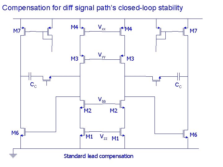
Compensation for diff signal path’s closed-loop stability M 4 M 7 Vxx M 4 Vyy M 3 M 7 M 3 CC CC Vbb M 2 M 6 M 1 M 2 Vzz M 1 Standard lead compensation M 6

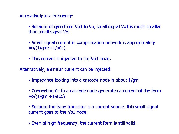
At relatively low frequency: • Because of gain from Vo 1 to Vo, small signal Vo 1 is much smaller than small signal Vo. • Small signal current in compensation network is approximately Vo/(1/gmz+1/s. Cc). • This current is injected to the Vo 1 node. Alternatively, a similar current can be injected: • Impedance looking into a cascode node is about 1/gm • Connecting Cc to a cascode node generates a current of the form Vo/(1/gm +1/s. Cc) • Because the base transistor is a current source, this small signal current goes to the Vo 1 node • Even at high frequency, the current form is still valid.

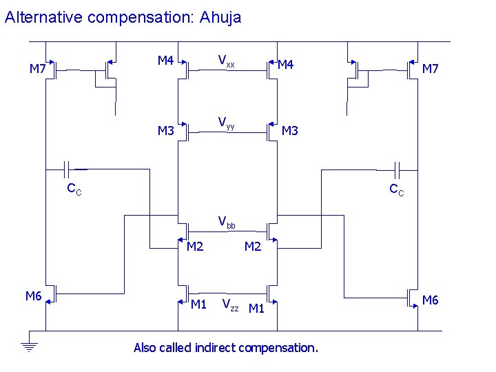
Alternative compensation: Ahuja M 4 M 7 Vxx M 4 Vyy M 3 M 7 M 3 CC CC Vbb M 2 M 6 M 1 M 2 Vzz M 1 Also called indirect compensation. M 6

In the Cc+Mz connection, • Bias voltage of Mz can be matched to track bias voltage of M 6 robustness to process and temperature variations • Size of Mz can be parameter scanned so as to place zero to cancel the secondary pole of the amplifier In the Cc to cascode connection, • Bias voltage can still be derived using current mirrors from a single current source, still have process and temperature tracking • But size of cascode transistor is determined based on folded cascode stage design • Cannot arbitrarily choose its size without considerations for output impedance at Vo 1, gain of op amp, and so on.

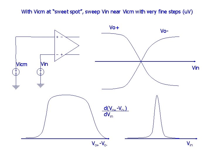
With Vicm at “sweet spot”, sweep Vin near Vicm with very fine steps (u. V) Vo+ Vicm Vin Vo- Vin d(Vo+-Vo-) d. Vin Vo+-Vo- Vin