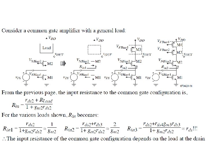
Common Gate Amplifiers Low Rin amplifier For input


, we can consider an Rs")


<<Vov If Vosp=Vosn=0")


DVo ÞDVGS 2= ro 1(gm")

- Slides: 34
Common Gate Amplifiers • Low Rin amplifier – For input impedance matching • Cascode amplifier – For I/O isolation (reducing effective Cgd) – For ro and Av enhancement
Common Gate Amplifier Ideal voltage source input
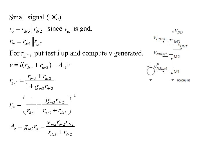
Questions: • All Vin’s have internal resistance Rs. What conditions must Rs satisfy in order for Vin to be treated as a voltage source? • What conditions must Rs satisfy if we want to use a current source input? • Which way is easier to satisfy? • With Rs, calculate ro for the third case. What conditions must Rs satisfy in order for ro to be large? When can we ignore the Rs effect?
Frequency Response
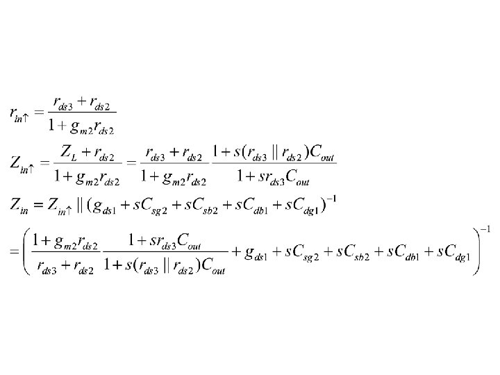
Questions • If the input has internal impedance Zs(s), we can consider an Rs in parallel with Cs. The parasitic caps at D 1 can no longer be ignored. Re-derive the transfer function from either Vin or Iin to Vout. • To obtain a general result, and to simplify, consider a general load from Vout looking up as RL and CL.
CMOS CASCODE AMPLIFIERS VDD Rb Rb Vin CL M 1 Vbb Vin M 2 M 1 CL Vout-min increase by VON 2 Vout-max decreased if a Cascoded source used Output swing is a big Problem in low voltage Applications
Cascoded current source load VDD Vyy Vxx Vbb Vin M 4 M 3 M 2 M 1 Q: How should you set the bias? Q: what is Vout-max? ro = AV = CL ro at D 1? v. D 1 = vin
Gain bandwidth product • If |p 1| << |p 2|, |p 3|, …, |p 1| << |z 1|, |z 2|, … – BW ≈ |p 1| – GBW ≈ gm 1/Co • Otherwise – AV(s) ≈ AV/(s/p 1+s/p 2…-s/z 1 -s/z 2… - 1) – 1/BW ≈ 1/p 1+2/p 2…-1/z 1 -2/z 2… = RC 1 + RC 2 + …
Any enhancement? Note: rds 2, Rb 1/ID 2 VDD gm 2 √ID 2 Effects on: Rb Vbb Vin ro, AV M 2 M 1 CL Co, GBW Slew rate
Folded cascoding Which I source should be cascoded? VDD ro, AV? M 1 Vin M 1 Vbb CL Co, GBW? Slew rate? poles? zeros?
Miller effect with high Rs input For example, Rs maybe the resistance seen by the gate of M 1 when resistive feedback is used. Cgd 1 sees a Miller effect by Av 1. At the gate, p=-1/Rs. Cgs, without Miller Becomes: p = 1/Rs(Cgs+Cgd*Av 1)
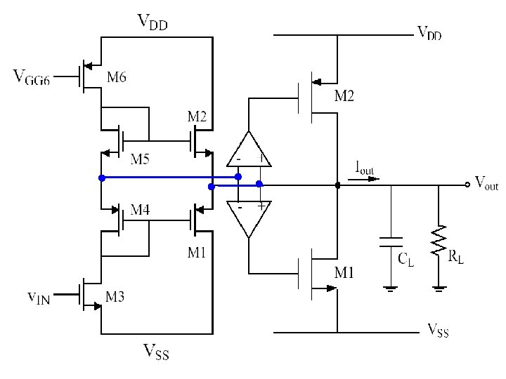
OUTPUT AMPLIFIERS • Requirements – Provide sufficient output power in the form of voltage or current. – Avoid signal distortion for large signal swings. – Be power efficient. – Provide protection from abnormal conditions. • Types of Output Stages – Class A amplifier. – Source follower. – Push-Pull amplifier ( inverting and follower). – Negative feedback (OP amp and resistive).
Power efficiency • It is most power efficient at maximum signal level • Let VSS= ─VDD, Vin is sinusoidal such that Vout reaches Voutmax • PRL = ½ (Voutmax)2/RL • Psupply>=average((VDD or VSS)*IRL) =VDD*average(Voutmax*sin()/RL) =2*VDD*Voutmax/RL/p • Power efficicy = PRL/Psupply<=p/4 (78%)
CLASS A AMPLIFIER ro, AV, z, p as before Power effic = PRL Psupply 0. 5 voutmax. IQ = I (V -V ) < 25% Q DD SS VSS= -VDD, Voutmax=VDD-Vdssat
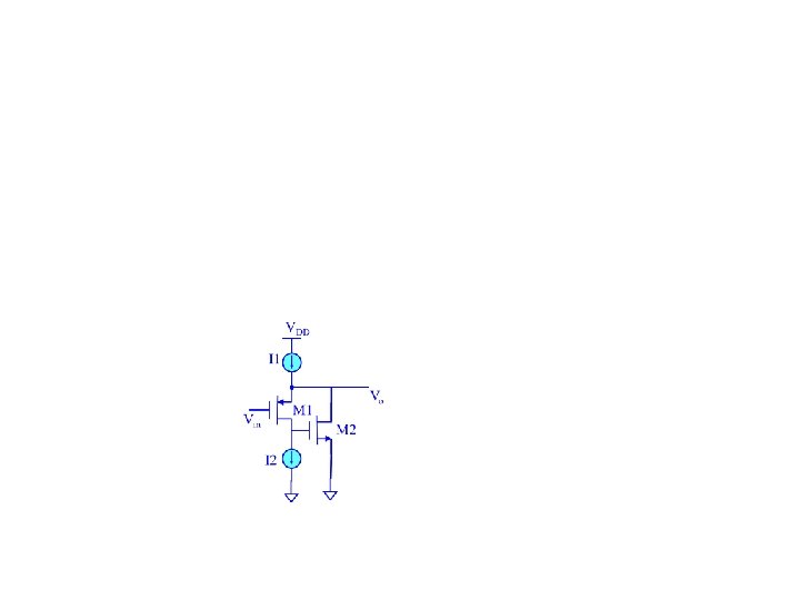
SOURCE FOLLOWER or VSS+VT
Push-pull
Push-pull inverting amp
Implementation
PUSH-PULL SOURCE FOLLOWER
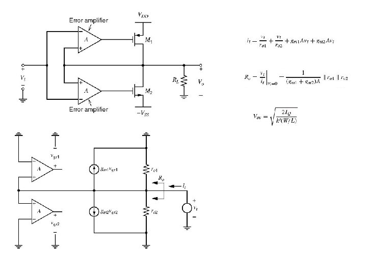
If Vo = 0 Bias current well controlled Vo swing is very limited
If A(Vosp-Vosn)<<Vov If Vosp=Vosn=0
Rin Rout
Combining the previous two: At quiescent, Vo=v 1+vgs 4 -vgs 1=v 1 This requires (W/L)1: W/L)2= (W/L)4: W/L)5
Example error amplifier M 15 is like a resistor connecting the drain and gate of M 17, leaving M 17 as level shifted diode connection. I 17 =Ib. By CM connection, I 13 = I 14 = m*Ib. I 11=I 12=Itail/2. I 15=I 16=I 13 -I 12=m*Ib-It/2. When vi != vo, I 12 varies from 0 to Itail. Hence, need m*Ib > Itail.
Super source follower DVo => DI 1 =(gm 1+gmb 1)DVo ÞDVGS 2= ro 1(gm 1+gmb 1)DVo ÞDI 2 = gm 2 ro 1(gm 1+gmb 1)DVo VDD I 1 Vo M 1 Vin M 2 I 2 go=gm 2 ro 1(gm 1+gmb 1) +(gm 1+gmb 1)+go 2 ≈gm 2 ro 1(gm 1+gmb 1) Gm ≈gm 1+gm 1 ro 1 gm 2 gm 1 AV=Gm/go≈ g + g m 1 mb 1 Ex: rework these when I 1 and I 2 have finite ro’s.
VDD If we re-arrange with a flipped version, we get this push-pull super source follower I 1 M 4 M 2 Vo M 1 Vin M 3 I 2 Ex: provide a transistor level implementation. Comment on power efficiency.