COMBLM 376 Computer Architecture Chapter 4 Cache Memory

COM/BLM 376 Computer Architecture Chapter 4 Cache Memory Asst. Prof. Dr. Gazi Erkan BOSTANCI ebostanci@ankara. edu. tr Slides are mainly based on Computer Organization and Architecture: Designing for Performance by William Stallings, 9 th Edition, Prentice Hall 1

Outline 1. Computer Memory System Overview 2. Cache Memory Principles 3. Elements of Cache Design 2

Although seemingly simple in concept, computer memory exhibits perhaps the widest range of type, technology, organization, performance, and cost of any feature of a computer system. No single technology is optimal in satisfying the memory requirements for a computer system. As a consequence, the typical computer system is equipped with a hierarchy of memory subsystems, some internal to the system (directly accessible by the processor) and some external (accessible by the processor via an I/O module). Here we examine cache memory which is an essential element of all modern computer systems. 3

Computer Memory System Overview Characteristics of Memory Systems 4

The term location refers to whether memory is internal and external to the computer. • Internal memory is often equated with main memory. But there are other forms of internal memory. • The processor requires its own local memory, in the form of registers. • Further, as we shall see, the control unit portion of the processor may also require its own internal memory. • External memory consists of peripheral storage devices, such as disk and tape, that are accessible to the processor via I/O controllers. 5

An obvious characteristic of memory is its capacity. For internal memory, this is typically expressed in terms of bytes (1 byte = 8 bits) or words. Common word lengths are 8, 16, and 32 bits. External memory capacity is typically expressed in terms of bytes. 6

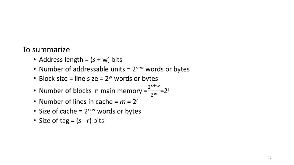
A related concept is the unit of transfer. For internal memory, the unit of transfer is equal to the number of electrical lines into and out of the memory module. This may be equal to the word length, but is often larger, such as 64, 128, or 256 bits. To clarify this point, consider three related concepts for internal memory: • Word: The “natural” unit of organization of memory. The size of a word is typically equal to the number of bits used to represent an integer and to the instruction length. Unfortunately, there are many exceptions. For example, the CRAY C 90 (an older model CRAY supercomputer) has a 64 -bit word length but uses a 46 -bit integer representation. The Intel x 86 architecture has a wide variety of instruction lengths, expressed as multiples of bytes, and a word size of 32 bits. • Addressable units: In some systems, the addressable unit is the word. However, many systems allow addressing at the byte level. In any case, the relationship between the length in bits A of an address and the number N of addressable units is 2 A = N. • Unit of transfer: For main memory, this is the number of bits read out of or written into memory at a time. The unit of transfer need not equal a word or an addressable unit. For external memory, data are often transferred in much larger units than a word, and these are referred to as blocks. 7

Method of accessing units of data. These include the following: • Sequential access: Memory is organized into units of data, called records. Access must be made in a specific linear sequence. Stored addressing information is used to separate records and assist in the retrieval process. • A shared read–write mechanism is used, and this must be moved from its current location to the desired location, passing and rejecting each intermediate record. Thus, the time to access an arbitrary record is highly variable. • Tape units 8

• Direct access: As with sequential access, direct access involves a shared read– write mechanism. However, individual blocks or records have a unique address based on physical location. • Access is accomplished by direct access to reach a general vicinity plus sequential searching, counting, or waiting to reach the final location. Again, access time is variable. • Disk units 9

• Random access: Each addressable location in memory has a unique, physically wired-in addressing mechanism. • The time to access a given location is independent of the sequence of prior accesses and is constant. Thus, any location can be selected at random and directly addressed and accessed. • Main memory and some cache systems are random access. 10

• Associative: This is a random access type of memory that enables one to make a comparison of desired bit locations within a word for a specified match, and to do this for all words simultaneously. • Thus, a word is retrieved based on a portion of its contents rather than its address. As with ordinary random-access memory, each location has its own addressing mechanism, and retrieval time is constant independent of location or prior access patterns. • Cache memories 11

• From a user’s point of view, the two most important characteristics of memory are capacity and performance. Three performance parameters are used: • Access time (latency): For random-access memory, this is the time it takes to perform a read or write operation, that is, the time from the instant that an address is presented to the memory to the instant that data have been stored or made available for use. For non-random-access memory, access time is the time it takes to position the read–write mechanism at the desired location. • Memory cycle time: This concept is primarily applied to random-access memory and consists of the access time plus any additional time required before a second access can commence. This additional time may be required for transients to die out on signal lines or to regenerate data if they are read destructively. Note that memory cycle time is concerned with the system bus, not the processor. 12

• Transfer rate: This is the rate at which data can be transferred into or out of a memory unit. For random-access memory, it is equal to 1/(cycle time). For non-random-access memory, the following relationship holds: where Tn = Average time to read or write n bits TA = Average access time n = Number of bits R = Transfer rate, in bits per second (bps) 13

• A variety of physical types of memory have been employed. The most common today are • semiconductor memory, • magnetic surface memory, used for disk and tape, and • optical and magneto-optical. 14

Several physical characteristics of data storage are important. • In a volatile memory, information decays naturally or is lost when electrical power is switched off. • In a nonvolatile memory, information once recorded remains without deterioration until deliberately changed; no electrical power is needed to retain information. • Magnetic-surface memories are nonvolatile. • Semiconductor memory (memory on integrated circuits) may be either volatile or nonvolatile. • Nonerasable memory cannot be altered, except by destroying the storage unit. Semiconductor memory of this type is known as read-only memory (ROM). • Of necessity, a practical nonerasable memory must also be nonvolatile. 15

The Memory Hierarchy The design constraints on a computer’s memory can be summed up by three questions: • How much? • How fast? • How expensive? 16

The question of how much is somewhat open ended. If the capacity is there, applications will likely be developed to use it. The question of how fast is, in a sense, easier to answer. To achieve greatest performance, the memory must be able to keep up with the processor. That is, as the processor is executing instructions, we would not want it to have to pause waiting for instructions or operands. For a practical system, the cost of memory must be reasonable in relationship to other components. 17

As might be expected, there is a trade-off among the three key characteristics of memory: capacity, access time, and cost. A variety of technologies are used to implement memory systems, and across this spectrum of technologies, the following relationships hold: • Faster access time, greater cost per bit • Greater capacity, smaller cost per bit • Greater capacity, slower access time The dilemma facing the designer is clear. • The designer would like to use memory technologies that provide for large-capacity memory, both because the capacity is needed and because the cost per bit is low. • However, to meet performance requirements, the designer needs to use expensive, relatively lower-capacity memories with short access times. 18

The way out of this dilemma is not to rely on a single memory component or technology, but to employ a memory hierarchy. As one goes down the hierarchy, the following occur: a. b. c. d. Decreasing cost per bit Increasing capacity Increasing access time Decreasing frequency of access of the memory by the processor 19

During the course of execution of a program, memory references by the processor, for both instructions and data, tend to cluster. Programs typically contain a number of iterative loops and subroutines. Once a loop or subroutine is entered, there are repeated references to a small set of instructions. Similarly, operations on tables and arrays involve access to a clustered set of data words. Over a long period of time, the clusters in use change, but over a short period of time, the processor is primarily working with fixed clusters of memory references. Accordingly, it is possible to organize data across the hierarchy such that the percentage of accesses to each successively lower level is substantially less than that of the level above. 20

Example Suppose that the processor has access to two levels of memory. • Level 1 contains 1000 words and has an access time of 0. 01 μs; level 2 contains 100, 000 words and has an access time of 0. 1 μs. Assume that if a word to be accessed is in level 1, then the processor accesses it directly. If it is in level 2, then the word is first transferred to level 1 and then accessed by the processor. For simplicity, we ignore the time required for the processor to determine whether the word is in level 1 or level 2. 21
 • If the")
• Performance of Accesses Involving only Level 1 (hit ratio) • If the accessed word is found in the faster memory, that is defined as a hit. A miss occurs if the accessed word is not found in the faster memory. 22

In our example, suppose 95% of the memory accesses are found in level 1. Then the average time to access a word can be expressed as (0. 95)(0. 01 µs) + (0. 05)(0. 01 µs + 0. 1 µs) = 0. 0095 + 0. 0055 = 0. 015 µs The average access time is much closer to 0. 01 μs than to 0. 1 μs, as desired. 23

Consider the two-level example already presented. Let level 2 memory contains all program instructions and data. The current clusters can be temporarily placed in level 1. From time to time, one of the clusters in level 1 will have to be swapped back to level 2 to make room for a new cluster coming in to level 1. On average, however, most references will be to instructions and data contained in level 1. 24

Cache Memory Principles Cache memory is designed to combine the memory access time of expensive, high speed memory combined with the large memory size of less expensive, lower-speed memory. 25

• There is a relatively large and slow main memory together with a smaller, faster cache memory. • When multiple levels of cache are used, the L 2 cache is slower and typically larger than the L 1 cache, and the L 3 cache is slower and typically larger than the L 2 cache. 26

Figure below depicts the structure of a cache/main-memory system. Main memory consists of up to 2 n addressable words, with each word having a unique n-bit address. For mapping purposes, this memory is considered to consist of a number of fixed-length blocks of K words each. That is, there are M = 2 n/K blocks in main memory. The cache consists of m blocks, called lines. Note that in referring to the basic unit of the cache, the term line is used, rather than the term block, for two reasons: 1. to avoid confusion with a main memory block, which contains the same number of data words as a cache line; and 2. because a cache line includes not only K words of data, just as a main memory block, but also includes tag and control bits. 27

28

Each line contains K words, plus a tag of a few bits. Each line also includes control bits (not shown), such as a bit to indicate whether the line has been modified since being loaded into the cache. The length of a line, not including tag and control bits, is the line size. 29

The line size may be as small as 32 bits, with each “word” being a single byte; in this case the line size is 4 bytes. The number of lines is considerably less than the number of main memory blocks (m << M). At any time, some subset of the blocks of memory resides in lines in the cache. If a word in a block of memory is read, that block is transferred to one of the lines of the cache. Because there are more blocks than lines, an individual line cannot be uniquely and permanently dedicated to a particular block. Thus, each line includes a tag that identifies which particular block is currently being stored. The tag is usually a portion of the main memory address. 30

Cache Read Operation • RA: Read Address 31

Note that last two operations occur in parallel and reflect the organization shown in Figure below, which is typical of contemporary cache organizations. In this organization, the cache connects to the processor via data, control, and address lines. The data and address lines also attach to data and address buffers, which attach to a system bus from which main memory is reached. When a cache hit occurs, the data and address buffers are disabled and communication is only between processor and cache, with no system bus traffic. When a cache miss occurs, the desired address is loaded onto the system bus and the data are returned through the data buffer to both the cache and the processor. In other organizations, the cache is physically interposed between the processor and the main memory for all data, address, and control lines. In this latter case, for a cache miss, the desired word is first read into the cache and then transferred from cache to processor. 32

Typical Cache Organization 33

Elements of Cache Design We occasionally refer to the use of caches in high-performance computing (HPC). HPC deals with supercomputers and their software, especially for scientific applications that involve large amounts of data, vector and matrix computation, and the use of parallel algorithms. Cache design for HPC is quite different than for other hardware platforms and applications. Although there a large number of cache implementations, there a few basic design elements that serve to classify and differentiate cache architectures. 34

Elements of Cache Design 35

Cache Addresses Almost all nonembedded processors, and many embedded processors, support virtual memory. In essence, virtual memory is a facility that allows programs to address memory from a logical point of view, without regard to the amount of main memory physically available. When virtual memory is used, the address fields of machine instructions contain virtual addresses. For reads to and writes from main memory, a hardware memory management unit (MMU) translates each virtual address into a physical address in main memory. 36

When virtual addresses are used, the system designer may choose to place the cache between the processor and the MMU or between the MMU and main memory (Figure below). A logical cache, also known as a virtual cache, stores data using virtual addresses. The processor accesses the cache directly, without going through the MMU. A physical cache stores data using main memory physical addresses. 37

38

One obvious advantage of the logical cache is that cache access speed is faster than for a physical cache, because the cache can respond before the MMU performs an address translation. The disadvantage has to do with the fact that most virtual memory systems supply each application with the same virtual memory address space. That is, each application sees a virtual memory that starts at address 0. Thus, the same virtual address in two different applications refers to two different physical addresses. The cache memory must therefore be completely flushed with each application context switch, or extra bits must be added to each line of the cache to identify which virtual address space this address refers to. 39

Cache Size We would like the size of the cache to be large enough so that the overall average cost per bit is close to that of main memory alone and small enough so that the overall average access time is close to that of the cache alone. There are several other motivations for minimizing cache size. The larger the cache, the larger the number of gates involved in addressing the cache. The result is that large caches tend to be slightly slower than small ones— even when built with the same integrated circuit technology and put in the same place on chip and circuit board. The available chip and board area also limits cache size. 40

Cache Sizes of Some Processors a. Two values separated by a slash refer to instruction and data caches. b. Both caches are instruction only; no data caches. 41

Mapping Function Because there are fewer cache lines than main memory blocks, an algorithm is needed for mapping main memory blocks into cache lines. Further, a means is needed for determining which main memory block currently occupies a cache line. The choice of the mapping function dictates how the cache is organized. Three techniques can be used: • direct, • associative, and • set associative –not to be covered in this course. 42

For all three cases, the example includes the following elements: • The cache can hold 64 Kbytes. • Data are transferred between main memory and the cache in blocks of 4 bytes each. This means that the cache is organized as 16 K = 214 lines of 4 bytes. • The main memory consists of 16 Mbytes, with each byte directly addressable by a 24 -bit address (224 = 16 M). Thus, for mapping purposes, we can consider main memory to consist of 4 M blocks of 4 bytes each. 43

DIRECT MAPPING The simplest technique, known as direct mapping, maps each block of main memory into only one possible cache line. The mapping is expressed as i = j modulo m where i = cache line number j = main memory block number m = number of lines in the cache 44

Figure below shows the mapping for the first m blocks of main memory. Each one of these blocks of main memory maps into one unique line of the cache. The next m blocks of main memory map into the cache in the same fashion; that is, block Bm of main memory maps into line L 0 of cache, block Bm+1 maps into line L 1, and so on. 45

Mapping from Main Memory to Cache 46

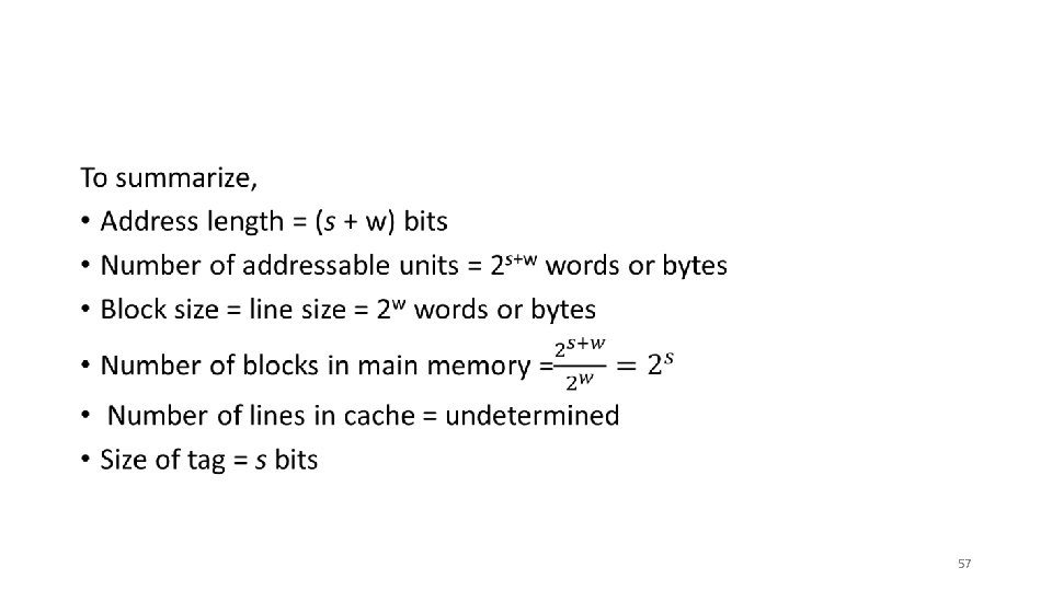
For purposes of cache access, each main memory address can be viewed as consisting of three fields: • The least significant w bits identify a unique word or byte within a block of main memory; in most contemporary machines, the address is at the byte level. • The remaining s bits specify one of the 2 s blocks of main memory. The cache logic interprets these s bits as a tag of s - r bits (most significant portion) and a line field of r bits. • This latter field identifies one of the m = 2 r lines of the cache. 47

• The mapping function is easily implemented using the main memory address. 49

The effect of this mapping is that blocks of main memory are assigned to lines of the cache as follows: Thus, the use of a portion of the address as a line number provides a unique mapping of each block of main memory into the cache. When a block is actually read into its assigned line, it is necessary to tag the data to distinguish it from other blocks that can fit into that line. The most significant s - r bits serve this purpose. 50

Example m = 16 K = 214 lines and i = j modulo 214. 51

The mapping becomes Note that no two blocks that map into the same line number have the same tag number. Thus, blocks with starting addresses 000000, 010000, …, FF 0000 have tag numbers 00, 01, …, FF, respectively. 52

A read operation works as follows: • The cache system is presented with a 24 -bit address. The 14 -bit line number is used as an index into the cache to access a particular line. • If the 8 -bit tag number matches the tag number currently stored in that line, then the 2 -bit word number is used to select one of the 4 bytes in that line. • Otherwise, the 22 -bit tag-plus-line field is used to fetch a block from main memory. The actual address that is used for the fetch is the 22 -bit tag-plus-line concatenated with two 0 bits, so that 4 bytes are fetched starting on a block boundary. 53

The direct mapping technique is simple and inexpensive to implement. Its main disadvantage is that there is a fixed cache location for any given block. Thus, if a program happens to reference words repeatedly from two different blocks that map into the same line, then the blocks will be continually swapped in the cache, and the hit ratio will be low (a phenomenon known as thrashing). 54

ASSOCIATIVE MAPPING Associative mapping overcomes the disadvantage of direct mapping by permitting each main memory block to be loaded into any line of the cache (Figure above (b)). In this case, the cache control logic interprets a memory address simply as a Tag and a Word field. The Tag field uniquely identifies a block of main memory. To determine whether a block is in the cache, the cache control logic must simultaneously examine every line’s tag for a match. 55

Fully Associative Cache Organization Note that no field in the address corresponds to the line number, so that the number of lines in the cache is not determined by the address format. 56

Example A main memory address consists of a 22 -bit tag and a 2 -bit byte number. The 22 -bit tag must be stored with the 32 -bit block of data for each line in the cache. Note that it is the leftmost (most significant) 22 bits of the address that form the tag. Thus, the 24 -bit hexadecimal address 16339 C has the 22 -bit tag 058 CE 7. 58

This is easily seen in binary notation: 59

With associative mapping, there is flexibility as to which block to replace when a new block is read into the cache. Replacement algorithms are designed to maximize the hit ratio. The principal disadvantage of associative mapping is the complex circuitry required to examine the tags of all cache lines in parallel. To overcome this problem, set-associative mapping is introduced. This is beyond the scope of our course. 60

Replacement Algorithms Once the cache has been filled, when a new block is brought into the cache, one of the existing blocks must be replaced. For direct mapping, there is only one possible line for any particular block, and no choice is possible. For the associative and set-associative techniques, a replacement algorithm is needed. To achieve high speed, such an algorithm must be implemented in hardware. A number of algorithms have been tried. • • LRU FIFO LFU Random 61
: Replace that block in the set that has been in")
LRU (Least Recently Used): Replace that block in the set that has been in the cache longest with no reference to it. For two-way set associative, this is easily implemented. Each line includes a USE bit. When a line is referenced, its USE bit is set to 1 and the USE bit of the other line in that set is set to 0. When a block is to be read into the set, the line whose USE bit is 0 is used. Because we are assuming that more recently used memory locations are more likely to be referenced, LRU should give the best hit ratio. LRU is also relatively easy to implement for a fully associative cache. The cache mechanism maintains a separate list of indexes to all the lines in the cache. When a line is referenced, it moves to the front of the list. For replacement, the line at the back of the list is used. Because of its simplicity of implementation, LRU is the most popular replacement algorithm. 62
: Replace that block in the set that has been in the cache")
FIFO (First-In-First-Out): Replace that block in the set that has been in the cache longest. FIFO is easily implemented as a round-robin or circular buffer technique. LFU (Least Frequently Used): Replace that block in the set that has experienced the fewest references. LFU could be implemented by associating a counter with each line. Random: Pick a line at random from among the candidate lines. Simulation studies have shown that random replacement provides only slightly inferior performance to an algorithm based on usage. 63

Write Policy When a block that is resident in the cache is to be replaced, there are two cases to consider: 1. If the old block in the cache has not been altered, then it may be overwritten with a new block without first writing out the old block. 2. If at least one write operation has been performed on a word in that line of the cache, then main memory must be updated by writing the line of cache out to the block of memory before bringing in the new block. 64

A variety of write policies, with performance and economic trade-offs, is possible. There are two problems to contend with. First, more than one device may have access to main memory. For example, an I/O module may be able to read-write directly to memory. If a word has been altered only in the cache, then the corresponding memory word is invalid. Further, if the I/O device has altered main memory, then the cache word is invalid. A more complex problem occurs when multiple processors are attached to the same bus and each processor has its own local cache. Then, if a word is altered in one cache, it could conceivably invalidate a word in other caches. 65

The simplest technique is called write through. Using this technique, all write operations are made to main memory as well as to the cache, ensuring that main memory is always valid. Any other processor–cache module can monitor traffic to main memory to maintain consistency within its own cache. The main disadvantage of this technique is that it generates substantial memory traffic and may create a bottleneck. 66

An alternative technique, known as write back, minimizes memory writes. With write back, updates are made only in the cache. When an update occurs, a dirty bit, or use bit, associated with the line is set. Then, when a block is replaced, it is written back to main memory if and only if the dirty bit is set. The problem with write back is that portions of main memory are invalid, and hence accesses by I/O modules can be allowed only through the cache. This makes for complex circuitry and a potential bottleneck. 67

Example Consider a cache with a line size of 32 bytes and a main memory that requires 30 ns to transfer a 4 -byte word. For any line that is written at least once before being swapped out of the cache, what is the average number of times that the line must be written before being swapped out for a writeback cache to be more efficient that a write-through cache? For the write-back case, each dirty line is written back once, at swap-out time, taking 8 x 30 = 240 ns. For the write-through case, each update of the line requires that one word be written out to main memory, taking 30 ns. Therefore, if the average line that gets written at least once gets written more than 8 times before swap out, then write back is more efficient. 68
 has")
In a bus organization in which more than one device (typically a processor) has a cache and main memory is shared, a new problem is introduced. If data in one cache are altered, this invalidates not only the corresponding word in main memory, but also that same word in other caches (if any other cache happens to have that same word). Even if a write-through policy is used, the other caches may contain invalid data. A system that prevents this problem is said to maintain cache coherency. 69

Possible approaches to cache coherency include the following: • Bus watching with write through: Each cache controller monitors the address lines to detect write operations to memory by other bus masters. If another master writes to a location in shared memory that also resides in the cache memory, the cache controller invalidates that cache entry. This strategy depends on the use of a write-through policy by all cache controllers. • Hardware transparency: Additional hardware is used to ensure that all updates to main memory via cache are reflected in all caches. Thus, if one processor modifies a word in its cache, this update is written to main memory. In addition, any matching words in other caches are similarly updated. • Noncacheable memory: Only a portion of main memory is shared by more than one processor, and this is designated as noncacheable. In such a system, all accesses to shared memory are cache misses, because the shared memory is never copied into the cache. The noncacheable memory can be identified using chipselect logic or high-address bits. 70

Line Size Another design element is the line size. When a block of data is retrieved and placed in the cache, not only the desired word but also some number of adjacent words are retrieved. As the block size increases from very small to larger sizes, the hit ratio will at first increase because of the principle of locality, which states that data in the vicinity of a referenced word are likely to be referenced in the near future. As the block size increases, more useful data are brought into the cache. The hit ratio will begin to decrease, however, as the block becomes even bigger and the probability of using the newly fetched information becomes less than the probability of reusing the information that has to be replaced. 71

Two specific effects come into play: • Larger blocks reduce the number of blocks that fit into a cache. Because each block fetch overwrites older cache contents, a small number of blocks results in data being overwritten shortly after they are fetched. • As a block becomes larger, each additional word is farther from the requested word and therefore less likely to be needed in the near future. The relationship between block size and hit ratio is complex, depending on the locality characteristics of a particular program, and no definitive optimum value has been found. 72

Number of Caches When caches were originally introduced, the typical system had a single cache. More recently, the use of multiple caches has become the norm. Two aspects of this design issue concern the number of levels of caches and the use of unified versus split caches. 73

Multilevel Caches As logic density has increased, it has become possible to have a cache on the same chip as the processor: the on-chip cache. Compared with a cache reachable via an external bus, the on-chip cache reduces the processor’s external bus activity and therefore speeds up execution times and increases overall system performance. When the requested instruction or data is found in the on-chip cache, the bus access is eliminated. Because of the short data paths internal to the processor, compared with bus lengths, on-chip cache accesses will complete appreciably faster than would even zero-wait state bus cycles. Furthermore, during this period the bus is free to support other transfers. 74

The inclusion of an on-chip cache leaves open the question of whether an off-chip, or external, cache is still desirable. Typically, the answer is yes, and most contemporary designs include both on-chip and external caches. The simplest such organization is known as a two-level cache, with the internal cache designated as level 1 (L 1) and the external cache designated as level 2 (L 2). The reason for including an L 2 cache is the following: If there is no L 2 cache and the processor makes an access request for a memory location not in the L 1 cache, then the processor must access DRAM or ROM memory across the bus. 75

Due to the typically slow bus speed and slow memory access time, this results in poor performance. On the other hand, if an L 2 SRAM (static RAM) cache is used, then frequently the missing information can be quickly retrieved. If the SRAM is fast enough to match the bus speed, then the data can be accessed using a zero-wait state transaction, the fastest type of bus transfer. 76

Two features of contemporary cache design for multilevel caches are noteworthy: 1. For an off-chip L 2 cache, many designs do not use the system bus as the path for transfer between the L 2 cache and the processor, but use a separate data path, so as to reduce the burden on the system bus. 2. With the continued shrinkage of processor components, a number of processors now incorporate the L 2 cache on the processor chip, improving performance. With the increasing availability of on-chip area available for cache, most contemporary microprocessors have moved the L 2 cache onto the processor chip and added an L 3 cache. Originally, the L 3 cache was accessible over the external bus. More recently, most microprocessors have incorporated an on-chip L 3 cache. 77

Unified versus Split Caches When the on-chip cache first made an appearance, many of the designs consisted of a single cache used to store references to both data and instructions. More recently, it has become common to split the cache into two: one dedicated to instructions and one dedicated to data. These two caches both exist at the same level, typically as two L 1 caches. When the processor attempts to fetch an instruction from main memory, it first consults the instruction L 1 cache, and when the processor attempts to fetch data from main memory, it first consults the data L 1 cache. 78

• There are two potential advantages of a unified cache: • For a given cache size, a unified cache has a higher hit rate than split caches because it balances the load between instruction and data fetches automatically. That is, if an execution pattern involves many more instruction fetches than data fetches, then the cache will tend to fill up with instructions, and if an execution pattern involves relatively more data fetches, the opposite will occur. • Only one cache needs to be designed and implemented. 79
- Slides: 79