Combinational Logic Circuit Design 1 April 2020 BME
Combinational Logic Circuit Design 1 April 2020 BME 2206 – Logic Circuits Faculty of Applied Sciences and
Lecture Outline § Fundamentals of Logic Design § Logic circuits using NAND and NOR gates § Adders • Half Adders • Full Adders § Subtractors • Half Subtractors • Full Subtractors § Subtraction using Adders
Fundamentals of Logic Design § The design of a combinational circuit starts from the verbal outline of the problem and ends with a logic circuit diagram or a set of Boolean functions from which the Boolean function can be easily obtained. § The procedure involves the following steps: i. The problem is stated ii. The number of available input variables and required output variables is determined. iii. The input and output variable are assigned their letter symbol iv. The truth table that defines the required relationship between the inputs and the outputs is derived v. The simplified Boolean function for each output is obtained vi. The logic diagram is drawn
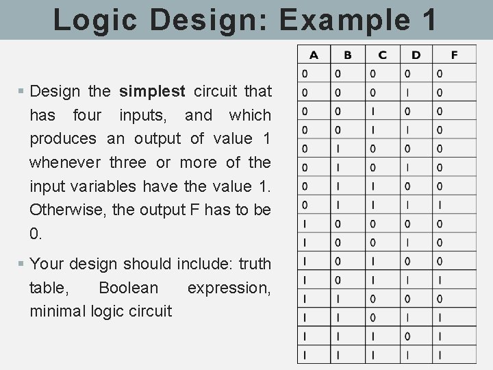
Logic Design: Example 1 § Design the simplest circuit that has four inputs, and which produces an output of value 1 whenever three or more of the input variables have the value 1. Otherwise, the output F has to be 0. § Your design should include: truth table, Boolean expression, minimal logic circuit
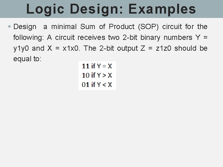
Logic Design: Examples § Design a minimal Sum of Product (SOP) circuit for the following: A circuit receives two 2 -bit binary numbers Y = y 1 y 0 and X = x 1 x 0. The 2 -bit output Z = z 1 z 0 should be equal to:
Logic with NAND & NOR § In addition to AND, OR, and NOT gates, other logic gates like NAND and NOR are also used in the design of digital circuits. § The NAND gate represents the complement of the AND operation. Its name is an abbreviation of NOT AND. § The graphic symbol for the NAND gate consists of an AND symbol with a bubble on the output, denoting that a complement operation is performed on the output of the AND gate as shown earlier § The NOR gate represents the complement of the OR operation. Its name is an abbreviation of NOT OR. § The graphic symbol for the NOR gate consists of an OR symbol with a bubble on the output, denoting that a complement operation is performed on the output of the OR gate as shown earlier.
Logic with NAND & NOR § A universal gate is a gate which can implement any Boolean function without the need to use any other gate type. § The NAND and NOR gates are universal gates. § In practice, this is advantageous since NAND and NOR gates are economical and easier to fabricate and are the basic gates used in all IC digital logic families. § In fact, an AND gate is typically implemented as a NAND gate followed by an inverter not the other way around. § Likewise, an OR gate is typically implemented as a NOR gate followed by an inverter not the other way around.
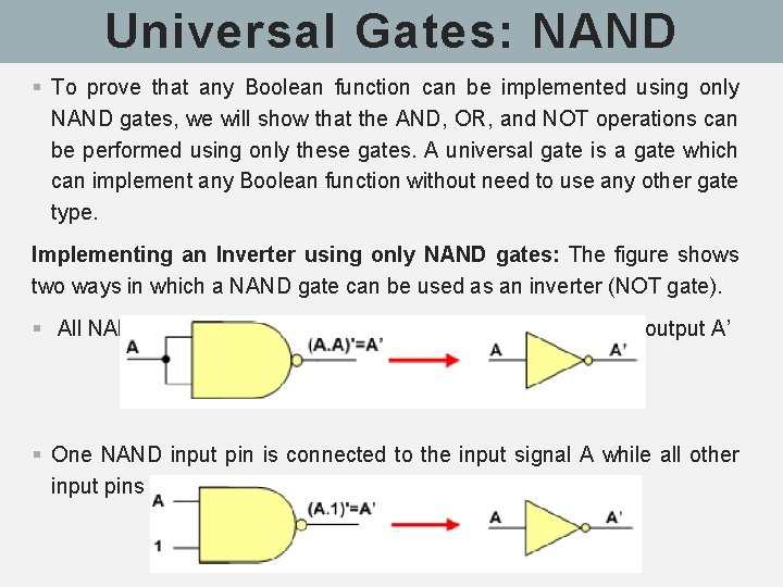
Universal Gates: NAND § To prove that any Boolean function can be implemented using only NAND gates, we will show that the AND, OR, and NOT operations can be performed using only these gates. A universal gate is a gate which can implement any Boolean function without need to use any other gate type. Implementing an Inverter using only NAND gates: The figure shows two ways in which a NAND gate can be used as an inverter (NOT gate). § All NAND input pins connected to the input signal A gives an output A’ § One NAND input pin is connected to the input signal A while all other input pins are connected to logic 1. The output will be A’
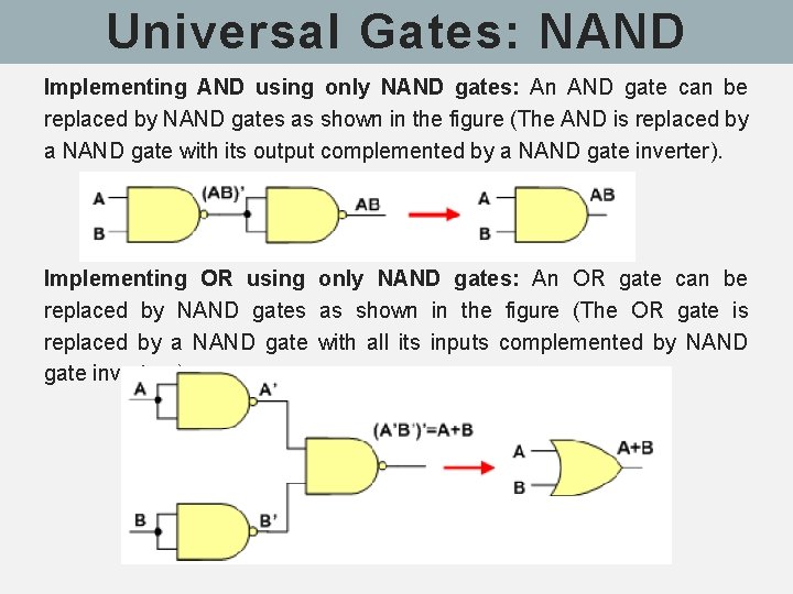
Universal Gates: NAND Implementing AND using only NAND gates: An AND gate can be replaced by NAND gates as shown in the figure (The AND is replaced by a NAND gate with its output complemented by a NAND gate inverter). Implementing OR using only NAND gates: An OR gate can be replaced by NAND gates as shown in the figure (The OR gate is replaced by a NAND gate with all its inputs complemented by NAND gate inverters).
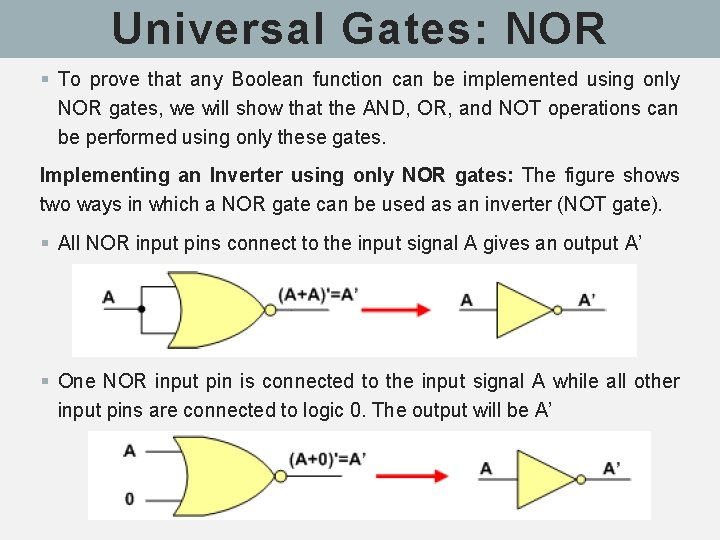
Universal Gates: NOR § To prove that any Boolean function can be implemented using only NOR gates, we will show that the AND, OR, and NOT operations can be performed using only these gates. Implementing an Inverter using only NOR gates: The figure shows two ways in which a NOR gate can be used as an inverter (NOT gate). § All NOR input pins connect to the input signal A gives an output A’ § One NOR input pin is connected to the input signal A while all other input pins are connected to logic 0. The output will be A’
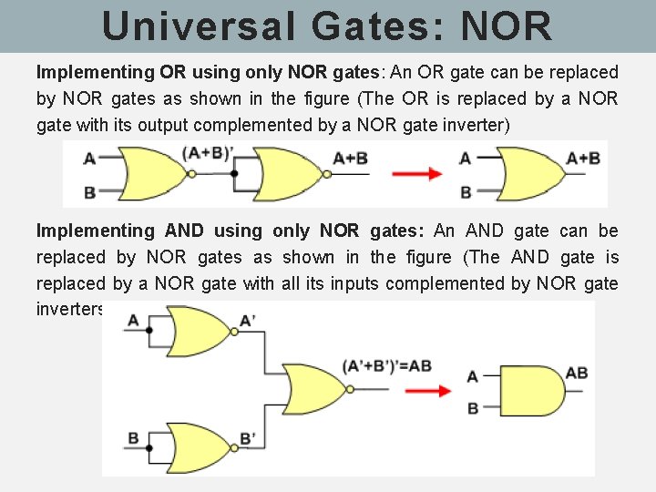
Universal Gates: NOR Implementing OR using only NOR gates: An OR gate can be replaced by NOR gates as shown in the figure (The OR is replaced by a NOR gate with its output complemented by a NOR gate inverter) Implementing AND using only NOR gates: An AND gate can be replaced by NOR gates as shown in the figure (The AND gate is replaced by a NOR gate with all its inputs complemented by NOR gate inverters)
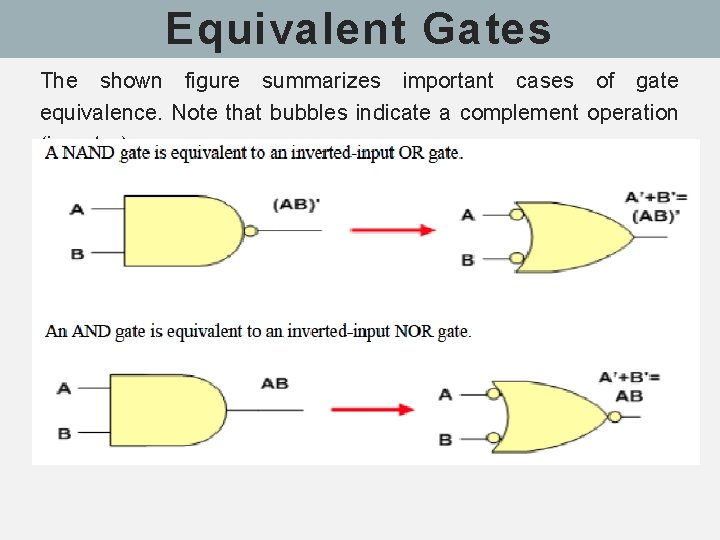
Equivalent Gates The shown figure summarizes important cases of gate equivalence. Note that bubbles indicate a complement operation (inverter).
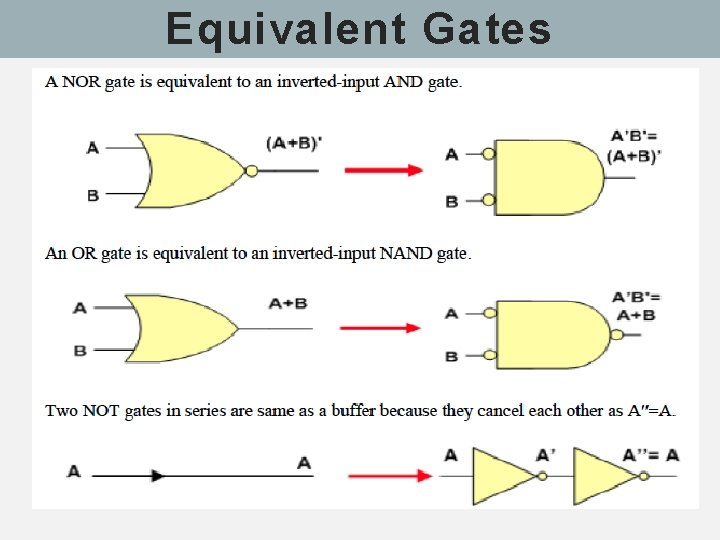
Equivalent Gates
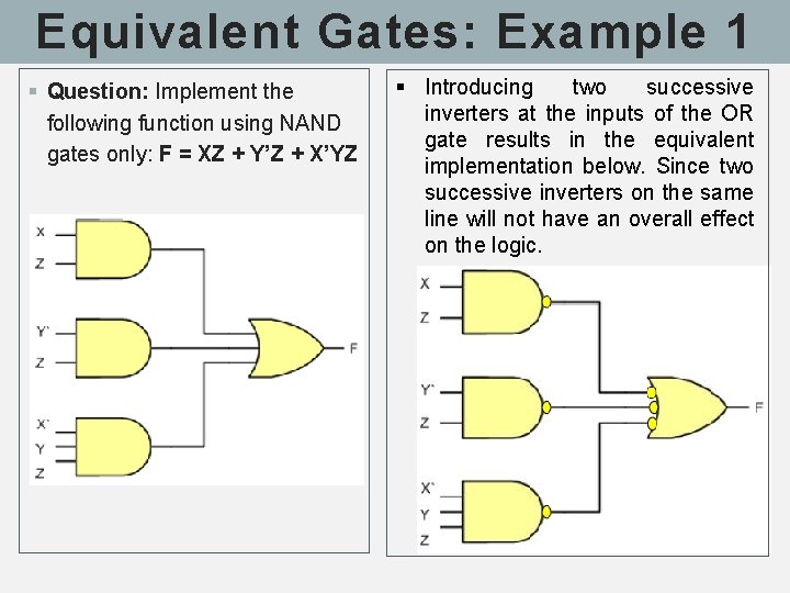
Equivalent Gates: Example 1 § Question: Implement the following function using NAND gates only: F = XZ + Y’Z + X’YZ § Introducing two successive inverters at the inputs of the OR gate results in the equivalent implementation below. Since two successive inverters on the same line will not have an overall effect on the logic.
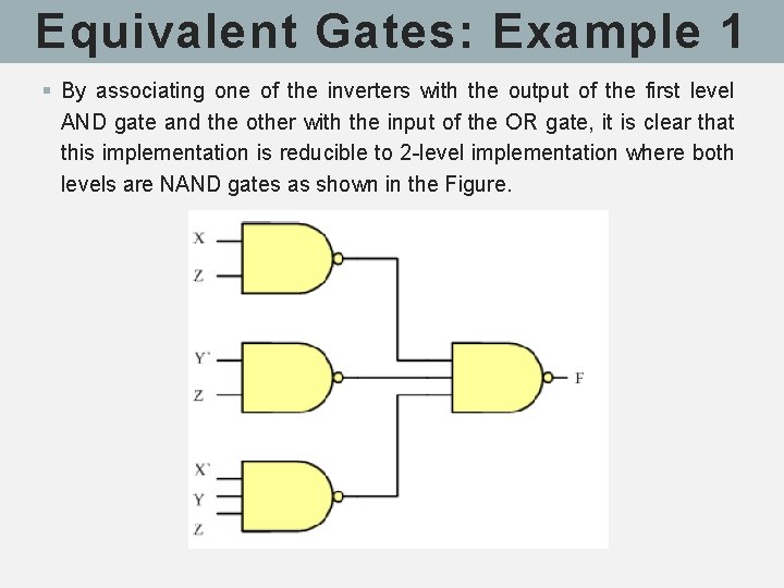
Equivalent Gates: Example 1 § By associating one of the inverters with the output of the first level AND gate and the other with the input of the OR gate, it is clear that this implementation is reducible to 2 -level implementation where both levels are NAND gates as shown in the Figure.
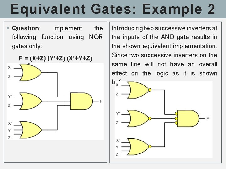
Equivalent Gates: Example 2 § Question: Implement the following function using NOR gates only: F = (X+Z) (Y’+Z) (X’+Y+Z) Introducing two successive inverters at the inputs of the AND gate results in the shown equivalent implementation. Since two successive inverters on the same line will not have an overall effect on the logic as it is shown before.
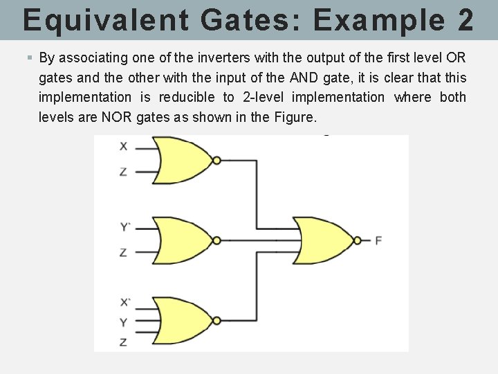
Equivalent Gates: Example 2 § By associating one of the inverters with the output of the first level OR gates and the other with the input of the AND gate, it is clear that this implementation is reducible to 2 -level implementation where both levels are NOR gates as shown in the Figure.
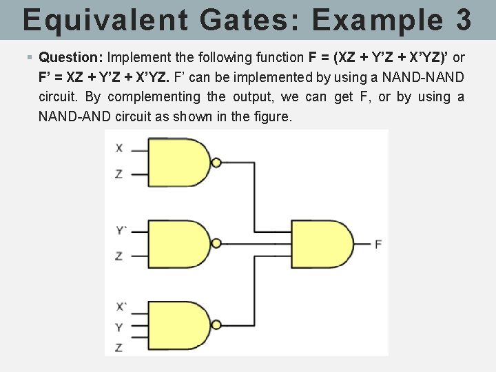
Equivalent Gates: Example 3 § Question: Implement the following function F = (XZ + Y’Z + X’YZ)’ or F’ = XZ + Y’Z + X’YZ. F’ can be implemented by using a NAND-NAND circuit. By complementing the output, we can get F, or by using a NAND-AND circuit as shown in the figure.
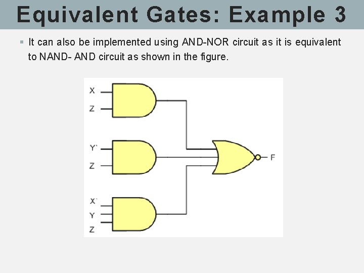
Equivalent Gates: Example 3 § It can also be implemented using AND-NOR circuit as it is equivalent to NAND- AND circuit as shown in the figure.
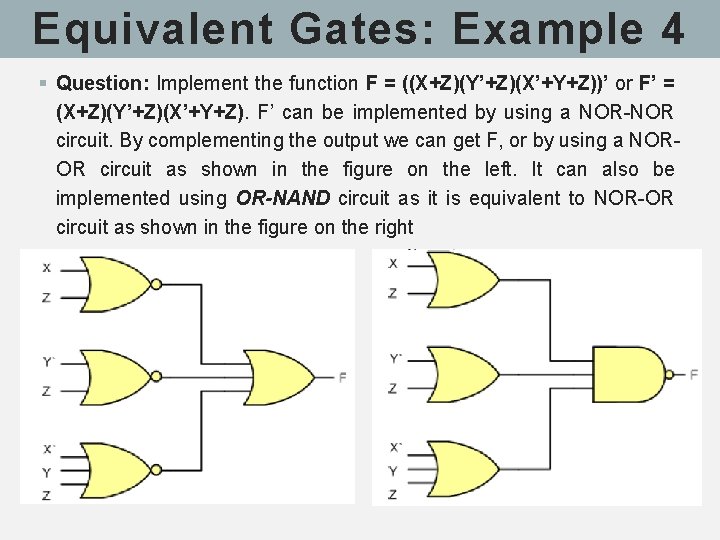
Equivalent Gates: Example 4 § Question: Implement the function F = ((X+Z)(Y’+Z)(X’+Y+Z))’ or F’ = (X+Z)(Y’+Z)(X’+Y+Z). F’ can be implemented by using a NOR-NOR circuit. By complementing the output we can get F, or by using a NOROR circuit as shown in the figure on the left. It can also be implemented using OR-NAND circuit as it is equivalent to NOR-OR circuit as shown in the figure on the right
Adders § Adders are an example of combinatorial circuits § In electronics, an adder or summer is a digital circuit that performs addition of numbers. § In modern computers, adders reside in the arithmetic logic unit (ALU) where other operations are performed. § Although adders can be constructed for many numerical representations, such as Binary-coded decimal or excess-3, the most common adders operate on binary numbers. § In cases where two’s complement or one’s complement is being used to represent negative numbers, it is trivial to modify an adder into an adder-subtracter. § Other signed number representations would require more complex adders.
Half Adders § A half adder is a logical circuit that performs an addition operation on two binary digits. § The half adder produces a sum and a carry value which are both binary digits. § A half adder has two inputs, generally labeled as A and B, and two outputs, the sum S and carry C. § S = two-bit XOR of A and B, and C = AND of A and B. § Essentially, the output of a half adder is the sum of 2 one-bit numbers, with C being the most significant of these two outputs. § The drawback of this circuit is that in case of a multiple bit addition, it cannot include a carry.
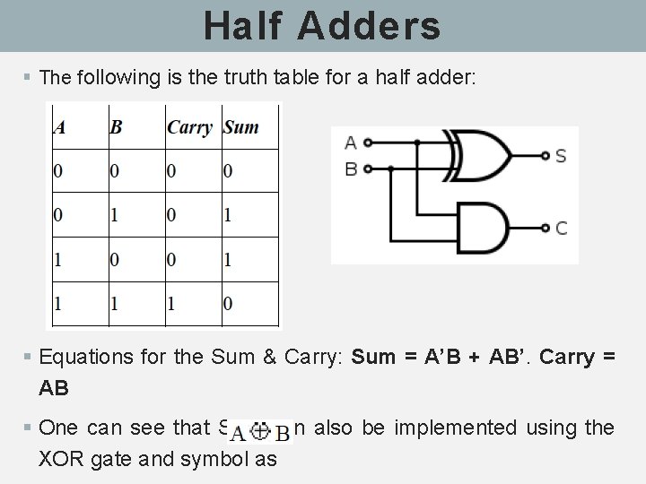
Half Adders § The following is the truth table for a half adder: § Equations for the Sum & Carry: Sum = A’B + AB’. Carry = AB § One can see that Sum can also be implemented using the XOR gate and symbol as
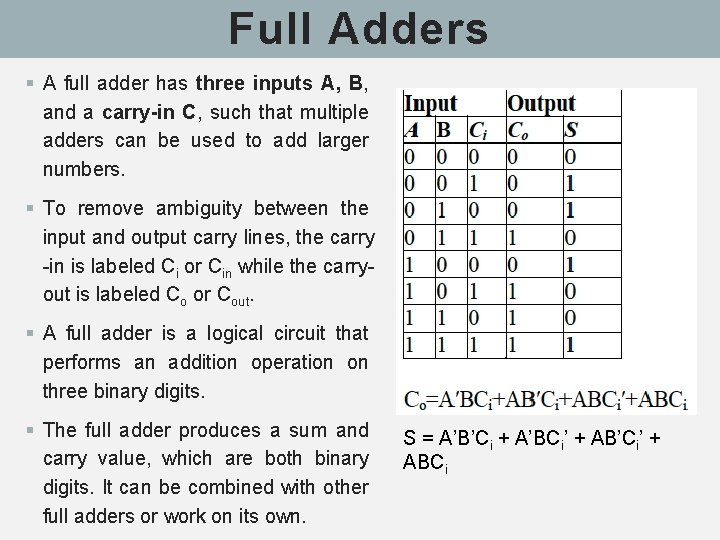
Full Adders § A full adder has three inputs A, B, and a carry-in C, such that multiple adders can be used to add larger numbers. § To remove ambiguity between the input and output carry lines, the carry -in is labeled Ci or Cin while the carryout is labeled Co or Cout. § A full adder is a logical circuit that performs an addition operation on three binary digits. § The full adder produces a sum and carry value, which are both binary digits. It can be combined with other full adders or work on its own. S = A’B’Ci + A’BCi’ + AB’Ci’ + ABCi
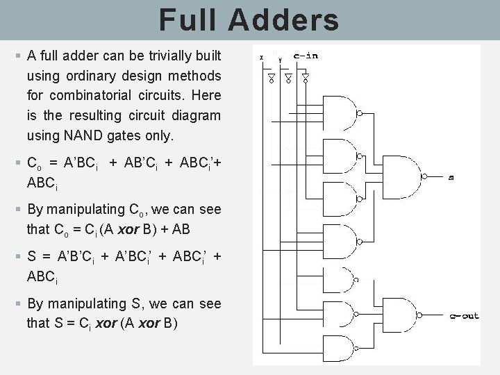
Full Adders § A full adder can be trivially built using ordinary design methods for combinatorial circuits. Here is the resulting circuit diagram using NAND gates only. § Co = A’BCi + AB’Ci + ABCi’+ ABCi § By manipulating Co, we can see that Co = Ci (A xor B) + AB § S = A’B’Ci + A’BCi’ + ABCi § By manipulating S, we can see that S = Ci xor (A xor B)
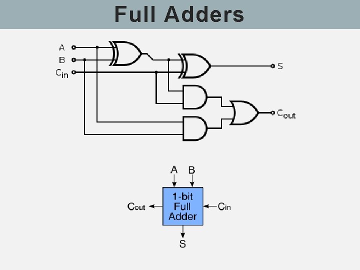
Full Adders § Note that the final OR gate before the carry-out output may be replaced by an XOR gate without altering the resulting logic. This is because the only discrepancy between OR and XOR gates occurs when both inputs are 1; for the adder shown here, this is never possible. § Using only two types of gates is convenient if one desires to implement the adder directly using common IC chips. § A full adder can be constructed from two half adders by connecting A and B to the input of one half adder, connecting the sum from that to an input of the second adder, connecting Ci to the other input and OR the two carry outputs. § Equivalently, S could be made three-bit xor of A, B, and Ci, and Co could be made three-bit majority function of A, B, and Ci. The output of the full adder is the two-bit arithmetic sum of 3 one-bit
Full Adders
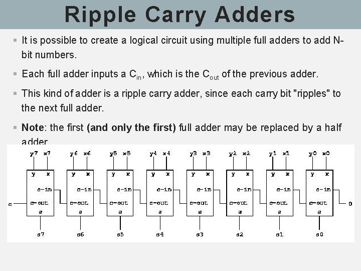
Ripple Carry Adders § It is possible to create a logical circuit using multiple full adders to add Nbit numbers. § Each full adder inputs a Cin, which is the Cout of the previous adder. § This kind of adder is a ripple carry adder, since each carry bit "ripples" to the next full adder. § Note: the first (and only the first) full adder may be replaced by a half adder.
Ripple Carry Adders § The layout of the ripple carry adder is simple, which allows for fast design time; however, it is relatively slow, since each full adder must wait for the carry bit to be calculated from the previous full adder. § The gate delay can easily be calculated by inspection of the full adder circuit. § Following the path from Cin to Cout shows 2 gates that must be passed through. § Therefore, a 32 -bit adder requires 31 carry computations and the final sum calculation for a total of 31 * 2 + 1 = 63 gate delays.
Subtractors § In electronics, a subtractor can be designed using the same approach as that of an adder. § The binary subtraction process is summarized below. : § As with an adder, in the general case of calculations on multi-bit numbers, three bits are involved in performing the subtraction for each bit: the minuend (Xi), subtrahend (Yi), and a borrow-in from the previous (less significant) bit order position (Bi). § The outputs are the difference bit (Di) and borrow bit Bi + 1.
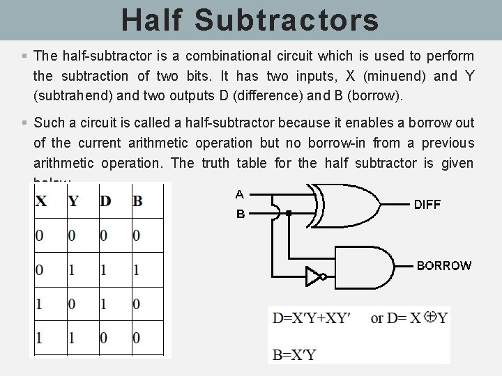
Half Subtractors § The half-subtractor is a combinational circuit which is used to perform the subtraction of two bits. It has two inputs, X (minuend) and Y (subtrahend) and two outputs D (difference) and B (borrow). § Such a circuit is called a half-subtractor because it enables a borrow out of the current arithmetic operation but no borrow-in from a previous arithmetic operation. The truth table for the half subtractor is given below.
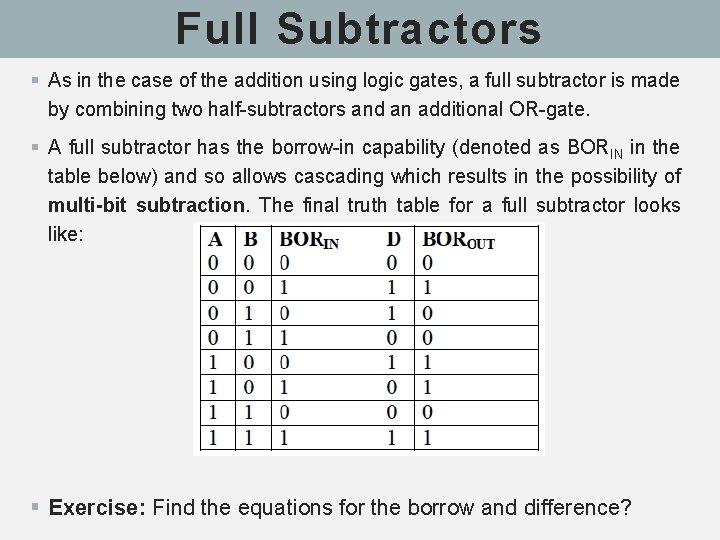
Full Subtractors § As in the case of the addition using logic gates, a full subtractor is made by combining two half-subtractors and an additional OR-gate. § A full subtractor has the borrow-in capability (denoted as BORIN in the table below) and so allows cascading which results in the possibility of multi-bit subtraction. The final truth table for a full subtractor looks like: § Exercise: Find the equations for the borrow and difference?
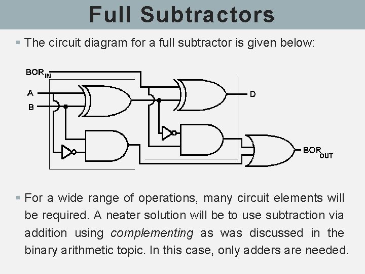
Full Subtractors § The circuit diagram for a full subtractor is given below: § For a wide range of operations, many circuit elements will be required. A neater solution will be to use subtraction via addition using complementing as was discussed in the binary arithmetic topic. In this case, only adders are needed.
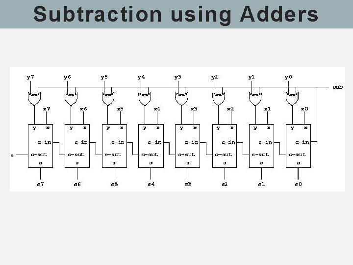
Subtraction using Adders § Our binary adder can already handle negative numbers as indicated in the section on binary arithmetic. But we have not discussed how we can get it to handle subtraction. § To see how this can be done, notice that in order to compute the expression X - Y, we can compute the expression X + -Y instead. § We know from the section on binary arithmetic how to negate a number by inverting all the bits and adding 1 (2’s complement). § Thus, we can compute the expression as X + inv(Y) + 1. It suffices to invert all the inputs of the second operand before they reach the adder, but how do we add the 1? That seems to require another adder just for that. § Luckily, we have an unused carry-in signal to position 0 that we can use. Giving a 1 on this input in effect adds one to the result. The complete circuit with addition and subtraction looks like this:
Subtraction using Adders

Exercise Generate the truth table and draw a logic circuit for a 3 -bit message parity checker and generator

Digital Integration § The purpose of circuit minimization is to obtain an algebraic expression that, when implemented results in a low cost circuit. Digital circuits are constructed with integrated circuits (ICs). An IC is a small silicon semiconductor crystal called chip containing the electronic component for digital gates. The various gates are interconnected inside the chip to form the required circuit. Digital ICs are categorized according to their circuit complexity as measured by the number of logic gates in a single package. i. Small scale integration (SSI): SSI devices contain fewer than 10 gates. The input and output of the gates are connected directly to the pins in the package. ii. Medium Scale Integration (MSI): MSI devices have the complexity of approximately 10 to 100 gates in a single package iii. Large Scale Integration (LSI): LSI devices contain between 100 and a few thousand gates in a single package iv. Very Large Scale Integration(VLSI): VLSI devices contain thousand of gates within a single package. VLSI devices have revolutionized the
- Slides: 37