Combinational Logic and Verilog Programmable Array Logic PAL
Combinational Logic and Verilog
Programmable Array Logic PAL
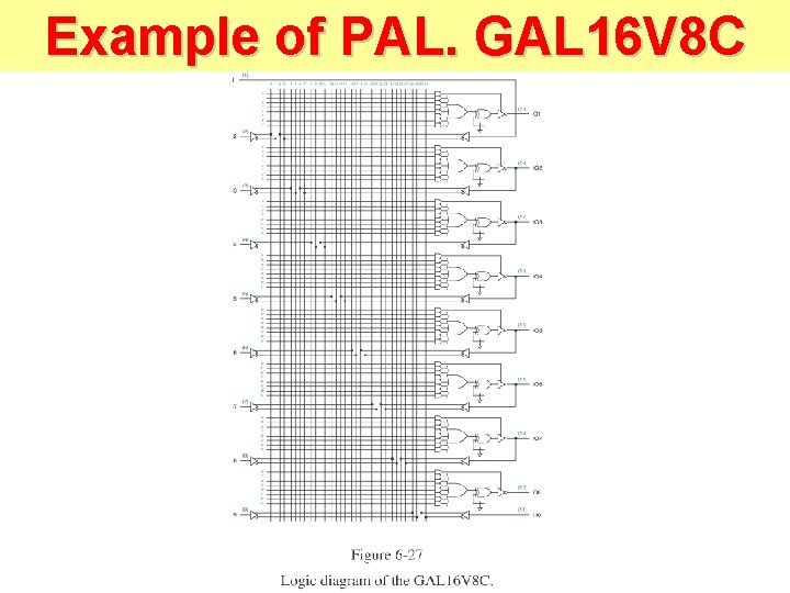
Example of PAL. GAL 16 V 8 C
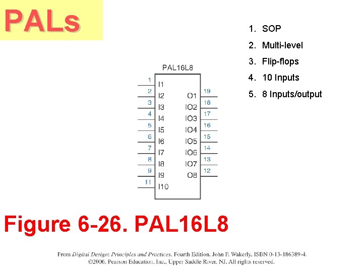
PALs 1. SOP 2. Multi-level 3. Flip-flops 4. 10 Inputs 5. 8 Inputs/output Figure 6 -26. PAL 16 L 8
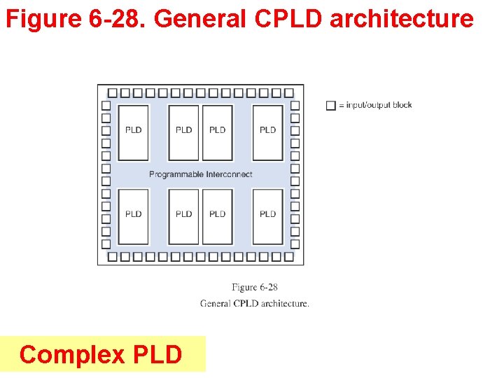
Figure 6 -28. General CPLD architecture Complex PLD
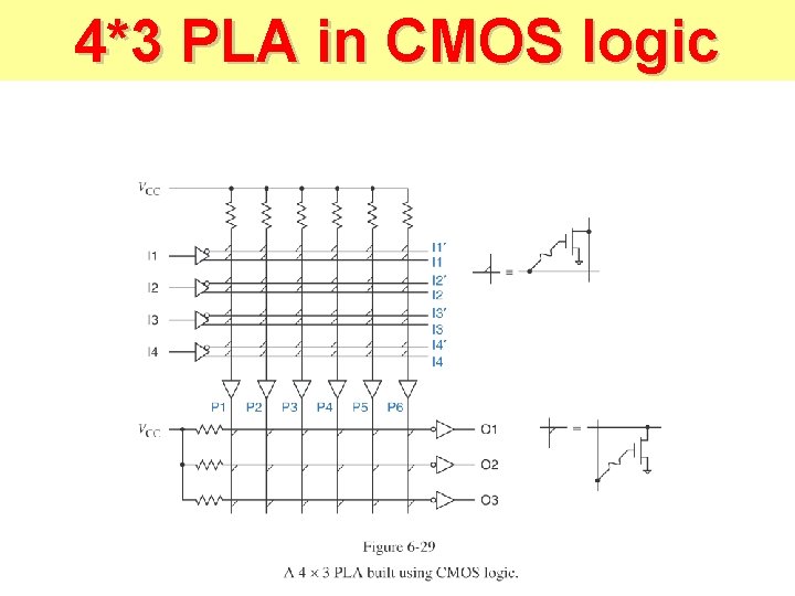
4*3 PLA in CMOS logic
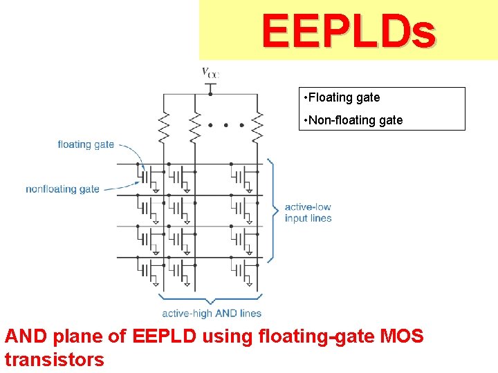
EEPLDs • Floating gate • Non-floating gate AND plane of EEPLD using floating-gate MOS transistors
Decoders
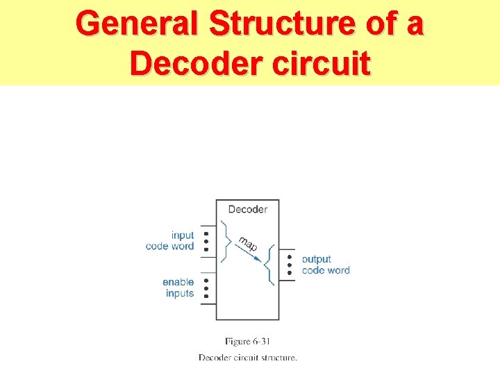
General Structure of a Decoder circuit
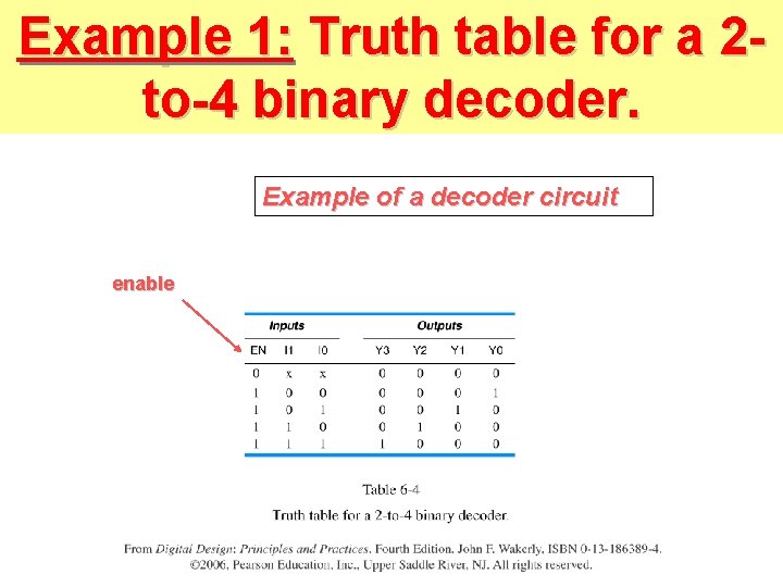
Example 1: Truth table for a 2 to-4 binary decoder. Example of a decoder circuit enable
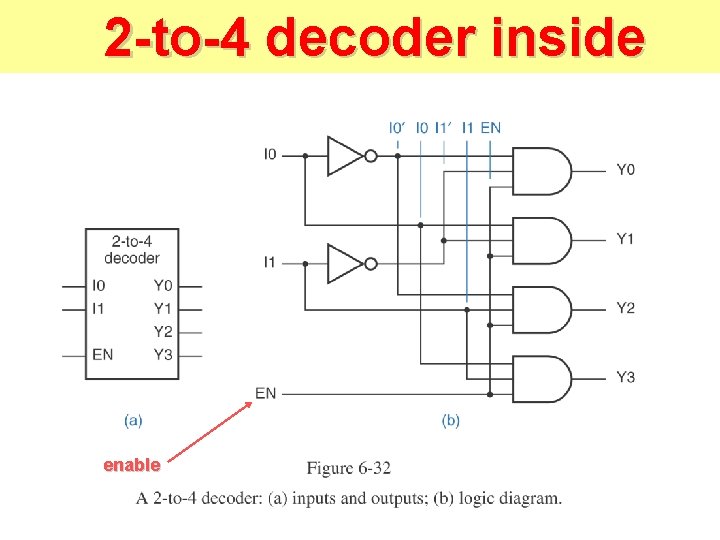
2 -to-4 decoder inside enable
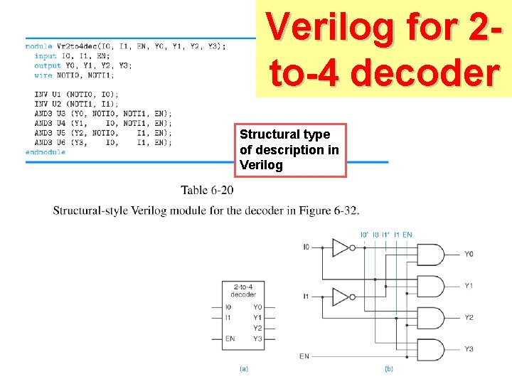
Verilog for 2 to-4 decoder Structural type of description in Verilog
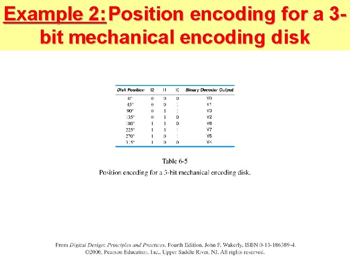
Example 2: Position encoding for a 3 bit mechanical encoding disk
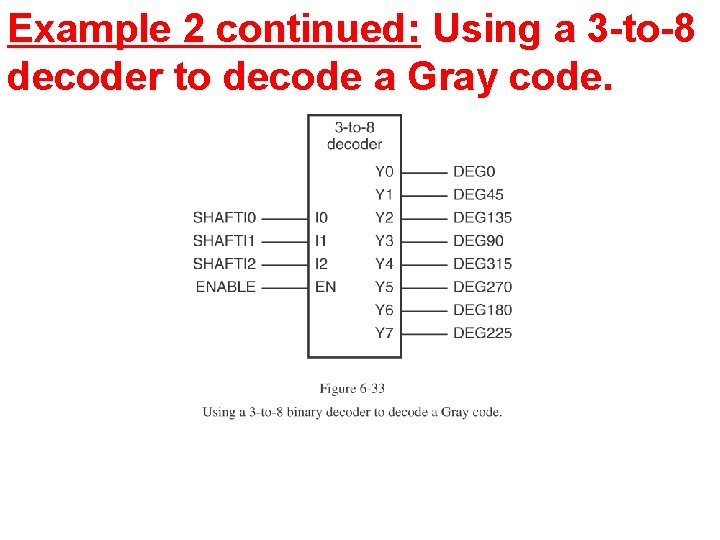
Example 2 continued: Using a 3 -to-8 decoder to decode a Gray code.
Example 3: 74 x 138 3 -to-8 decoder
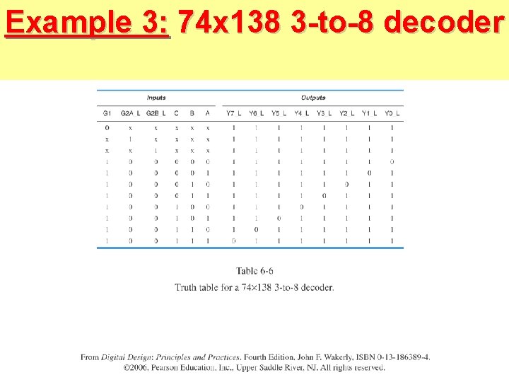
Example 3: 74 x 138 3 -to-8 decoder
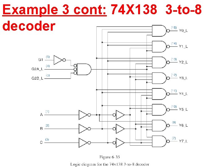
Example 3 cont: 74 X 138 3 -to-8 decoder
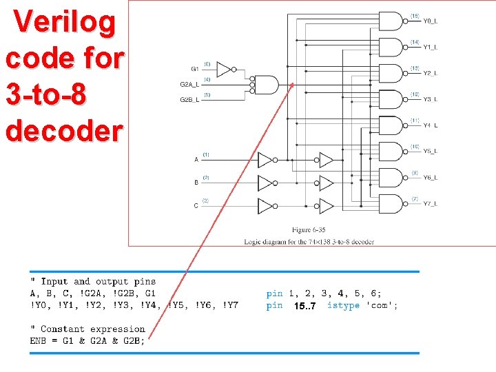
Verilog code for 3 -to-8 decoder 15. . 7
![Verilog for 3 -to-8 decoder Y_L[0] Y_L[1] Y_L[2] Y_L[3] A[2] Y_L[4] A[1] Y_L[5] A[0] Verilog for 3 -to-8 decoder Y_L[0] Y_L[1] Y_L[2] Y_L[3] A[2] Y_L[4] A[1] Y_L[5] A[0]](http://slidetodoc.com/presentation_image_h2/b433fc4f746757dfa18754c39f320bd1/image-19.jpg)
Verilog for 3 -to-8 decoder Y_L[0] Y_L[1] Y_L[2] Y_L[3] A[2] Y_L[4] A[1] Y_L[5] A[0] Y_L[7]
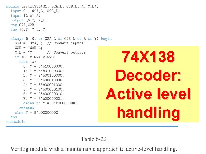
74 X 138 Decoder: Active level handling
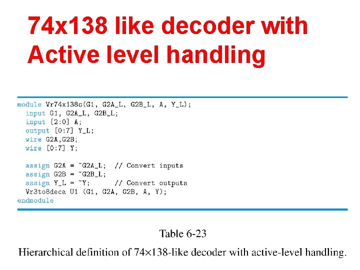
74 x 138 like decoder with Active level handling
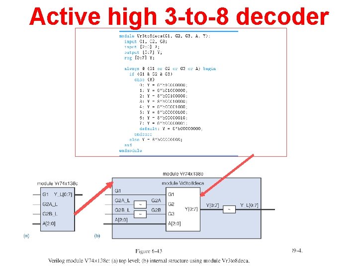
Active high 3 -to-8 decoder
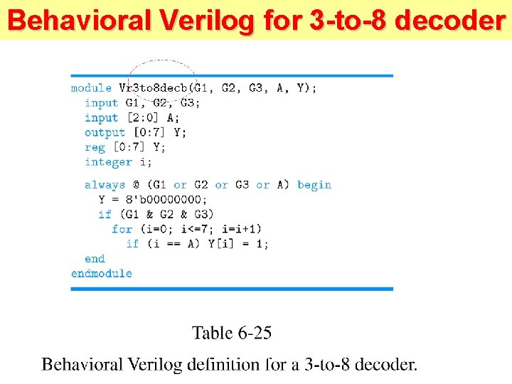
Behavioral Verilog for 3 -to-8 decoder
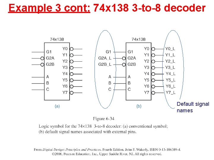
Example 3 cont: 74 x 138 3 -to-8 decoder Default signal names
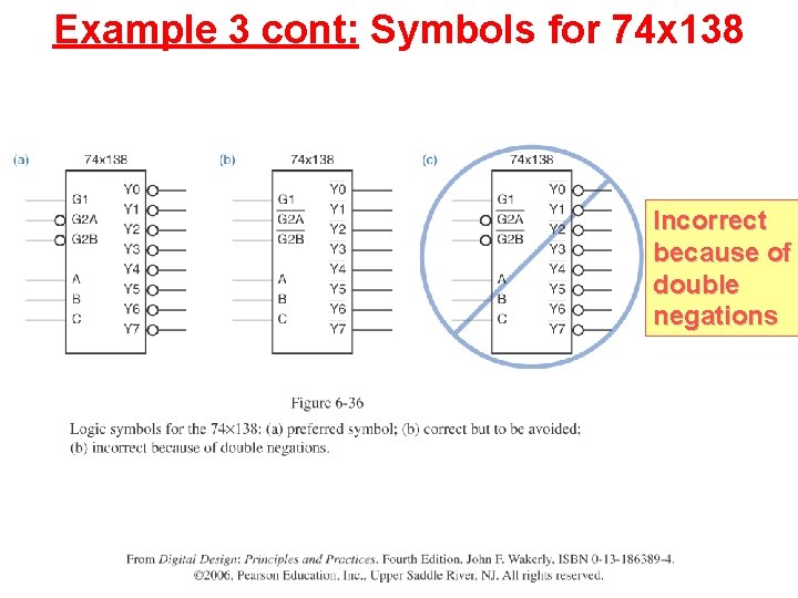
Example 3 cont: Symbols for 74 x 138 Incorrect because of double negations
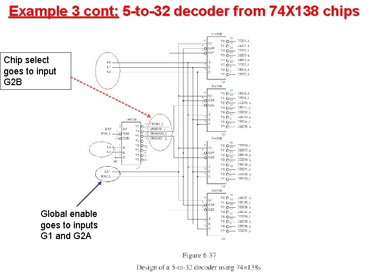
Example 3 cont: 5 -to-32 decoder from 74 X 138 chips Chip select goes to input G 2 B Global enable goes to inputs G 1 and G 2 A
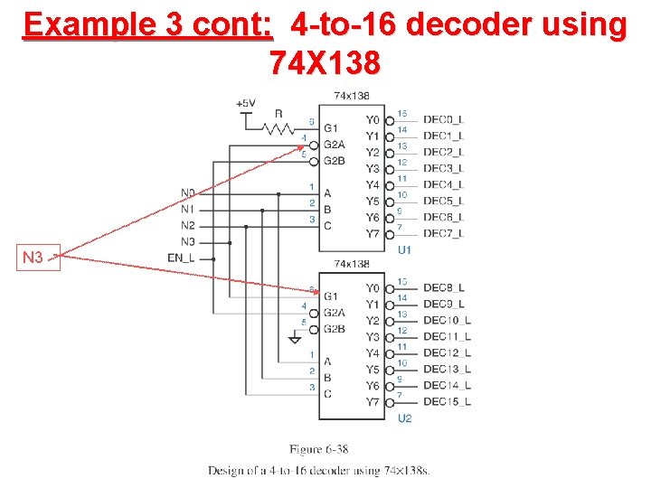
Example 3 cont: 4 -to-16 decoder using 74 X 138 N 3
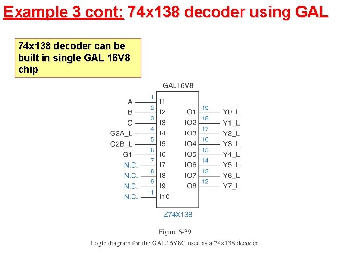
Example 3 cont: 74 x 138 decoder using GAL 74 x 138 decoder can be built in single GAL 16 V 8 chip
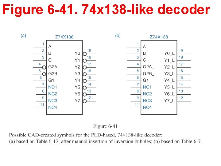
Figure 6 -41. 74 x 138 -like decoder
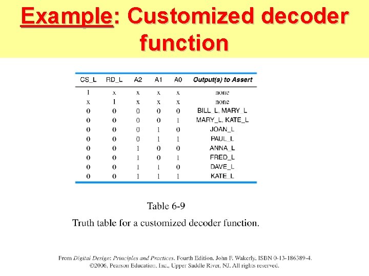
Example: Customized decoder function
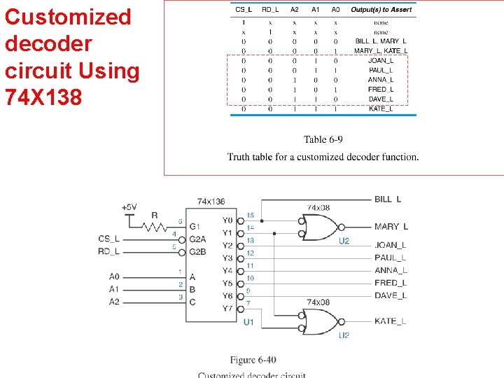
Customized decoder circuit Using 74 X 138
Seven Segment Display and Decoder
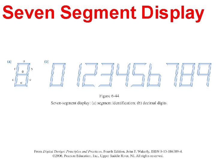
Seven Segment Display
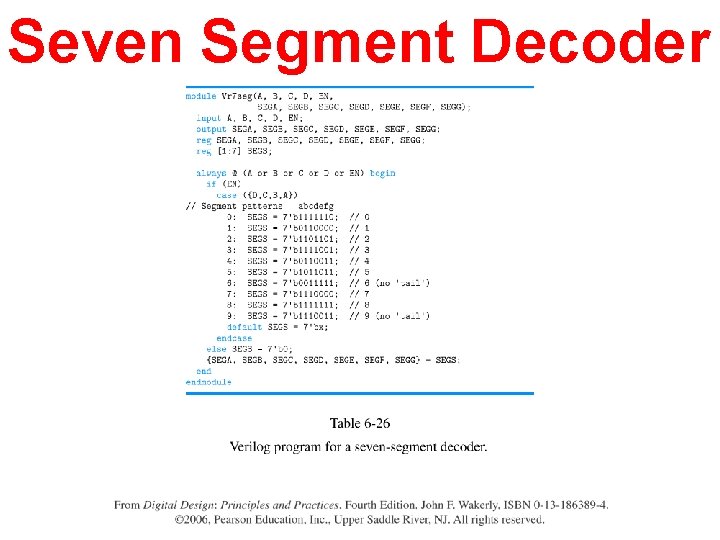
Seven Segment Decoder
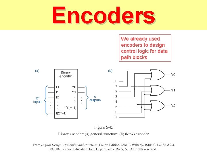
Encoders We already used encoders to design control logic for data path blocks
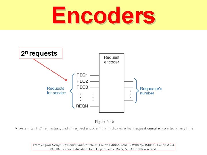
Encoders 2 n requests
Priority Encoders
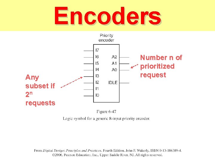
Encoders Any subset if 2 n requests Number n of prioritized request
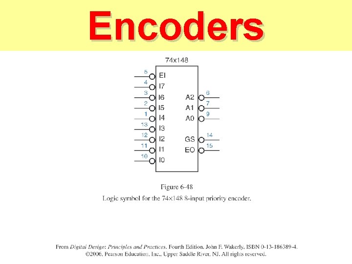
Encoders
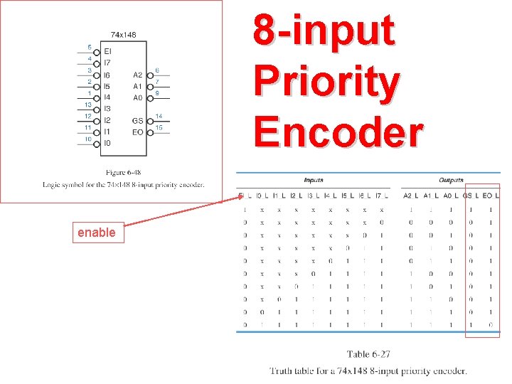
8 -input Priority Encoder enable
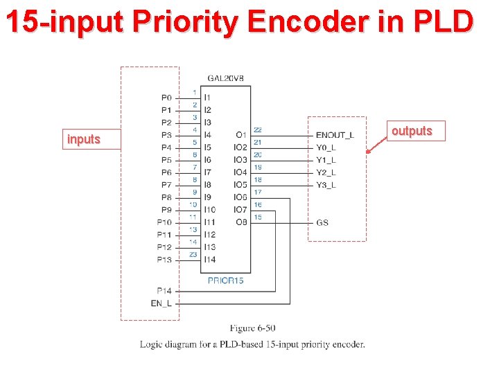
15 -input Priority Encoder in PLD inputs outputs
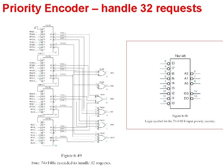
Priority Encoder – handle 32 requests
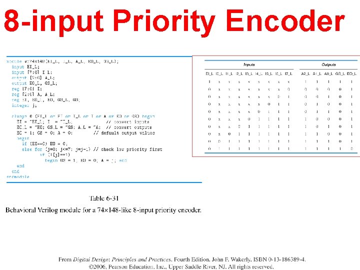
8 -input Priority Encoder

Three state Buffers
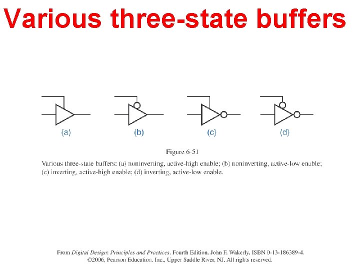
Various three-state buffers
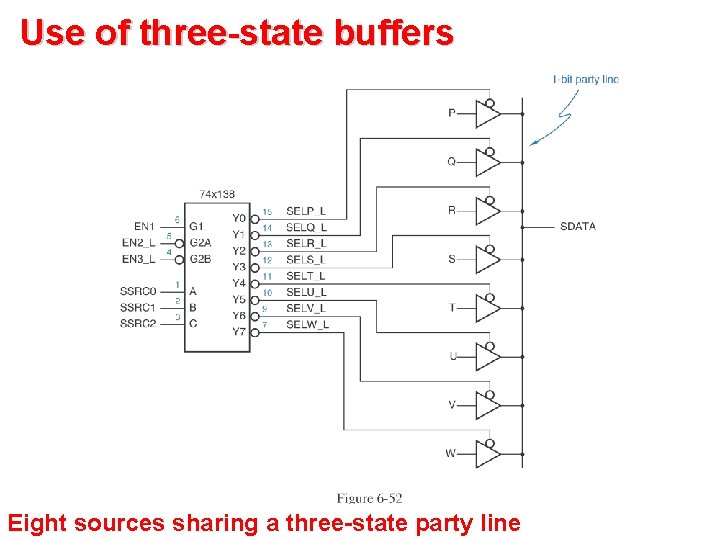
Use of three-state buffers Eight sources sharing a three-state party line
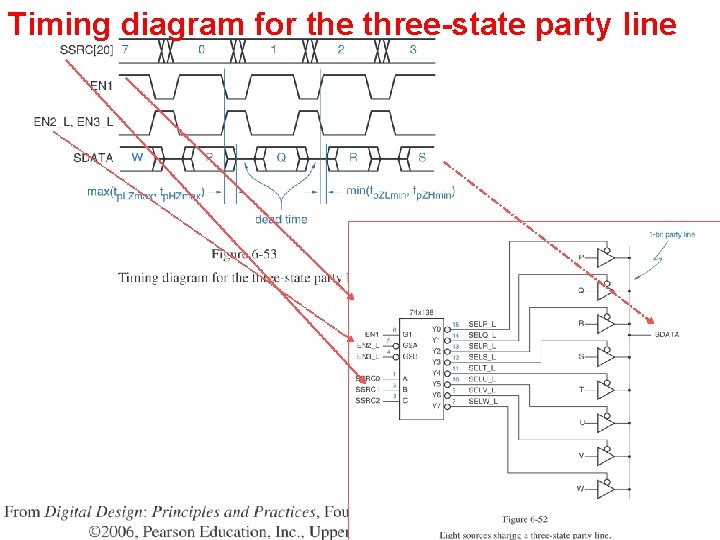
Timing diagram for the three-state party line
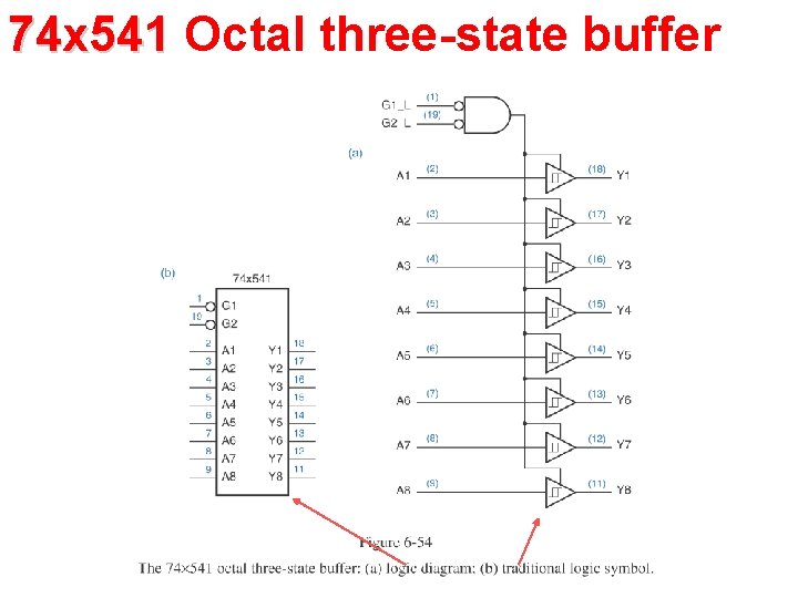
74 x 541 Octal three-state buffer
Three-State buffers in microprocessors
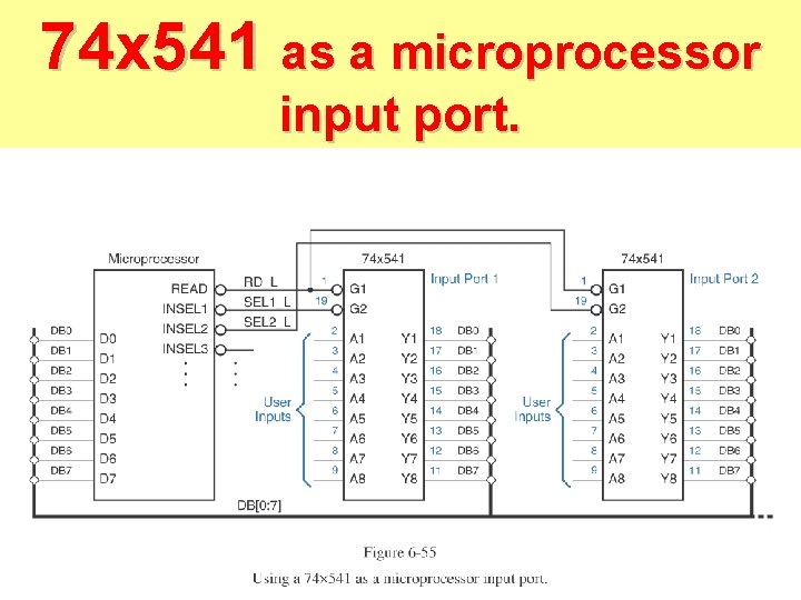
74 x 541 as a microprocessor input port.
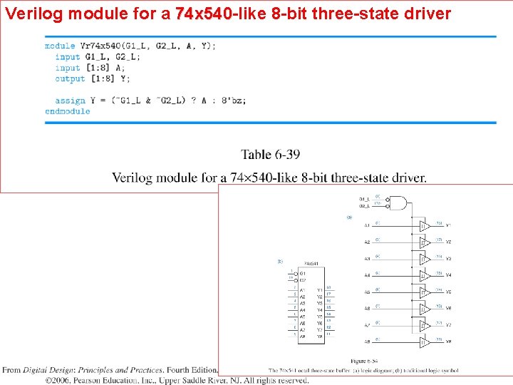
Verilog module for a 74 x 540 -like 8 -bit three-state driver 74 x 540
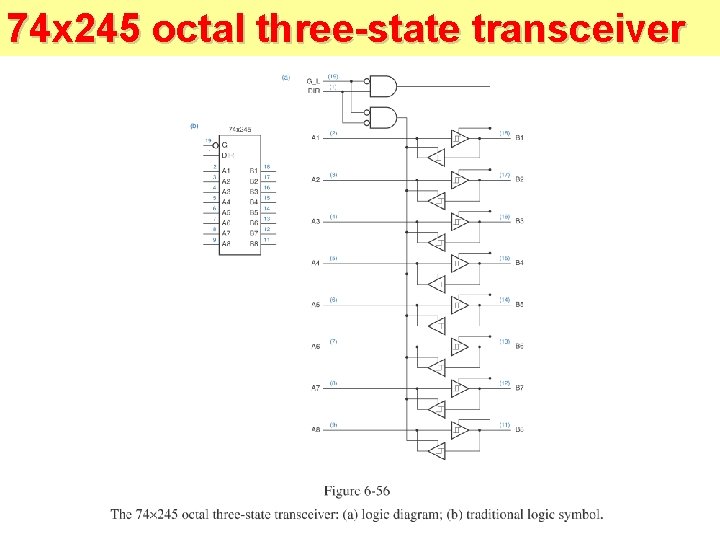
74 x 245 octal three-state transceiver
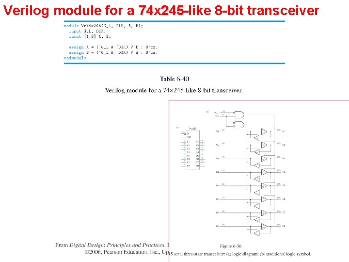
Verilog module for a 74 x 245 -like 8 -bit transceiver 74 x 245
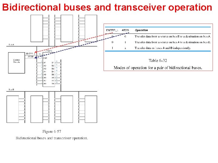
Bidirectional buses and transceiver operation
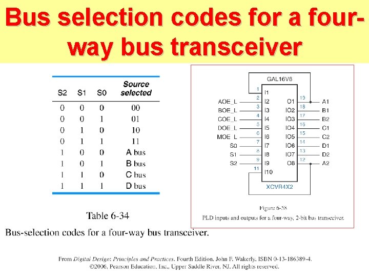
Bus selection codes for a fourway bus transceiver
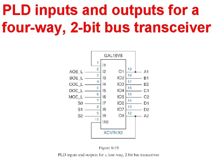
PLD inputs and outputs for a four-way, 2 -bit bus transceiver
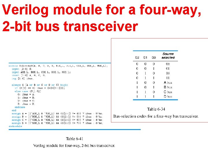
Verilog module for a four-way, 2 -bit bus transceiver
Multiplexers
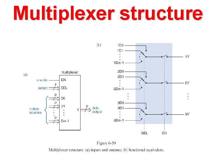
Multiplexer structure
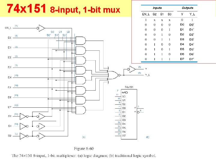
74 x 151 8 -input, 1 -bit mux
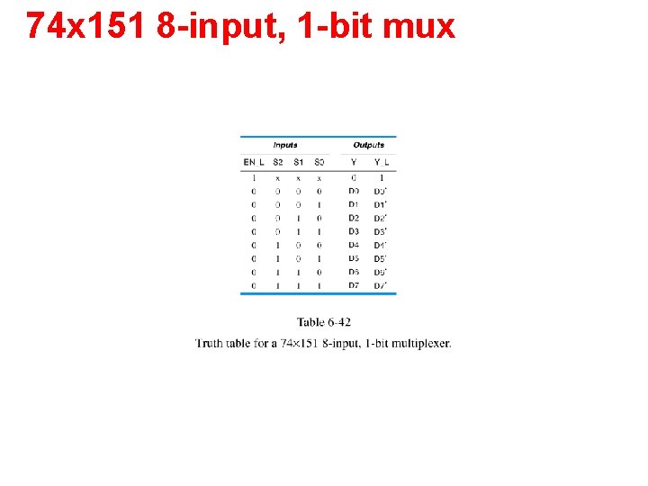
74 x 151 8 -input, 1 -bit mux
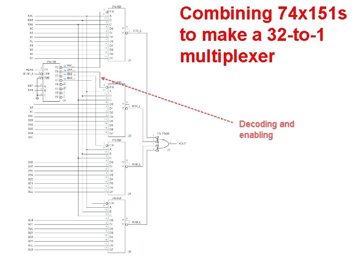
Combining 74 x 151 s to make a 32 -to-1 multiplexer Decoding and enabling
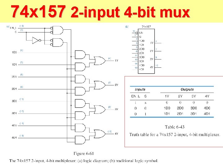
74 x 157 2 -input 4 -bit mux
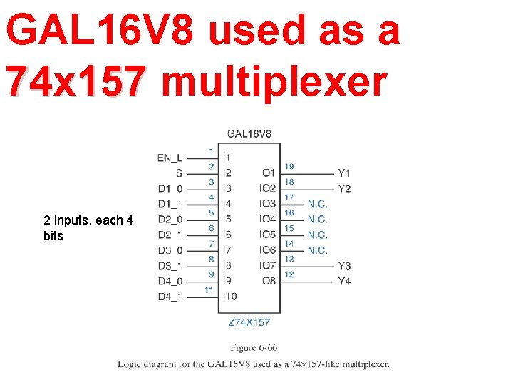
GAL 16 V 8 used as a 74 x 157 multiplexer 2 inputs, each 4 bits
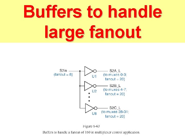
Buffers to handle large fanout
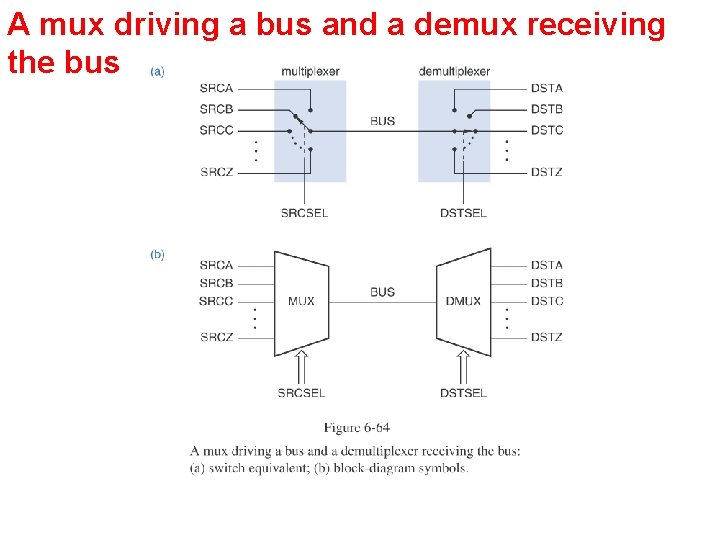
A mux driving a bus and a demux receiving the bus
Decoders as demultiplexers
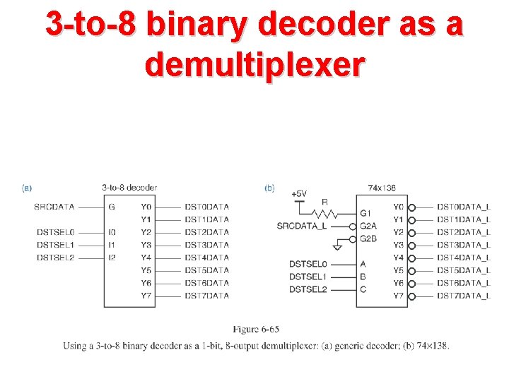
3 -to-8 binary decoder as a demultiplexer
GALs as multiplexers
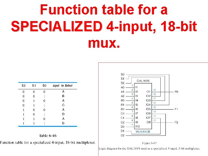
Function table for a SPECIALIZED 4 -input, 18 -bit mux.
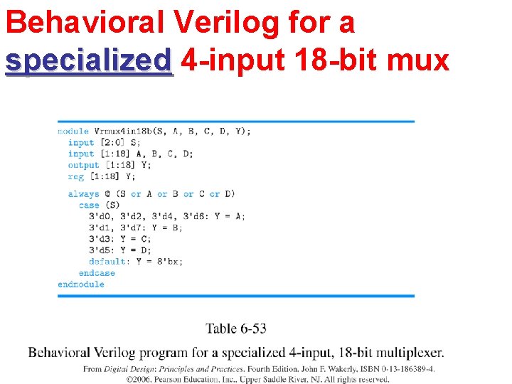
Behavioral Verilog for a specialized 4 -input 18 -bit mux
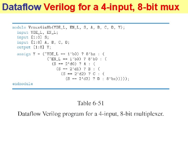
Dataflow Verilog for a 4 -input, 8 -bit mux
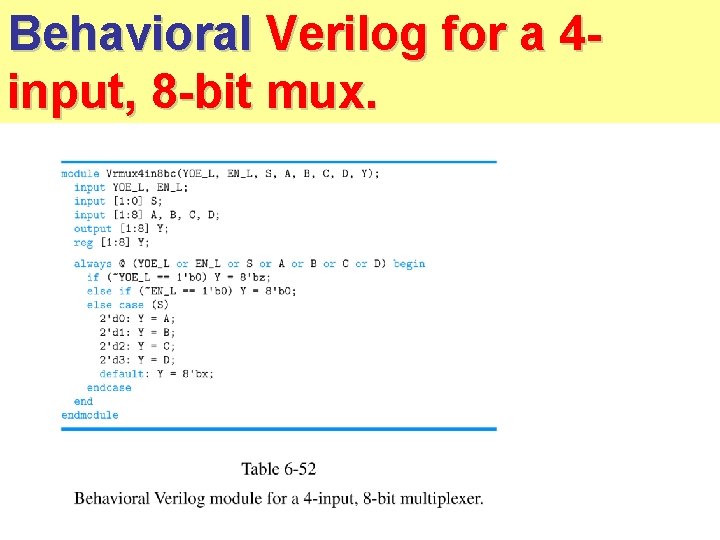
Behavioral Verilog for a 4 input, 8 -bit mux.
- Slides: 73