Combinational Design Part 2 Procedure Topics Positive vs
Combinational Design, Part 2: Procedure
Topics • Positive vs. negative logic • Design procedure 2
Positive and Negative Logic Two different assignments of signal levels to logic values are possible 1. Using H level to represent a logic 1 (true) defines a positive logic system 2. Using H level to represent a logic 0 (true) defines a negative logic system 3
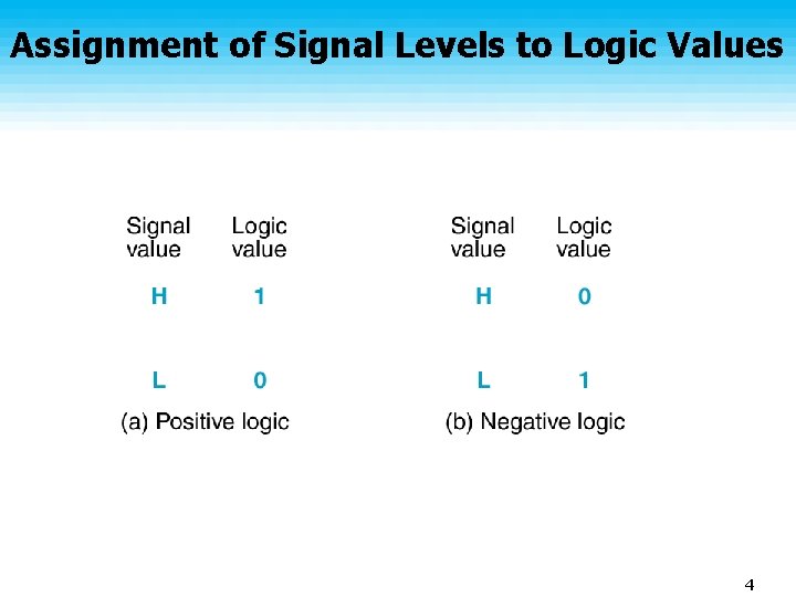
Assignment of Signal Levels to Logic Values 4
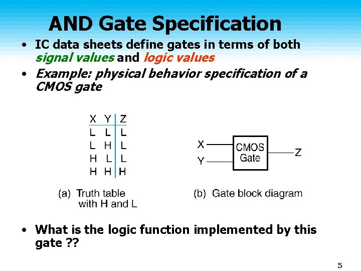
AND Gate Specification • IC data sheets define gates in terms of both signal values and logic values • Example: physical behavior specification of a CMOS gate • What is the logic function implemented by this gate ? ? 5
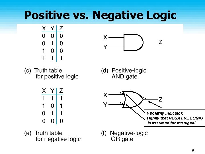
Positive vs. Negative Logic a polarity indicator: signify that NEGATIVE LOGIC is assumed for the signal 6
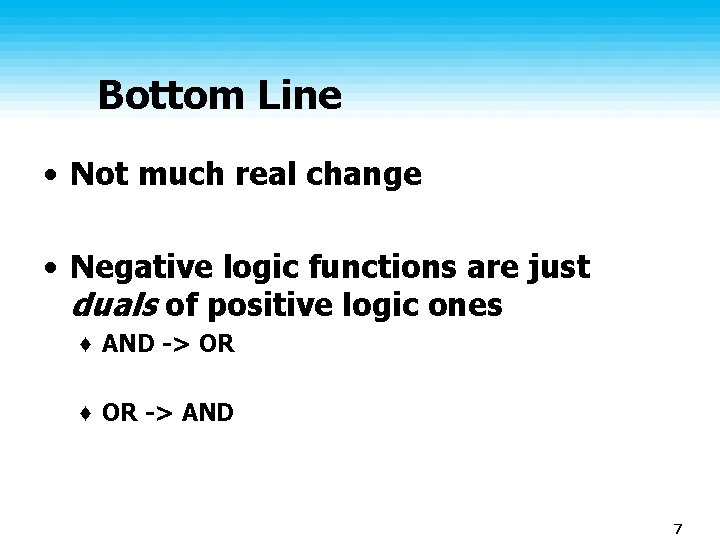
Bottom Line • Not much real change • Negative logic functions are just duals of positive logic ones ♦ AND -> OR ♦ OR -> AND 7
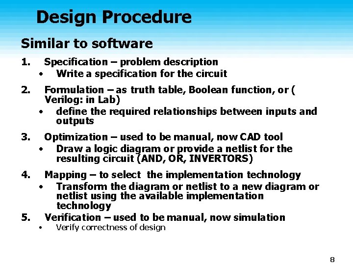
Design Procedure Similar to software 1. Specification – problem description • Write a specification for the circuit 2. Formulation – as truth table, Boolean function, or ( Verilog: in Lab) • define the required relationships between inputs and outputs 3. Optimization – used to be manual, now CAD tool • Draw a logic diagram or provide a netlist for the resulting circuit (AND, OR, INVERTORS) 4. Mapping – to select the implementation technology • Transform the diagram or netlist to a new diagram or netlist using the available implementation technology 5. Verification – used to be manual, now simulation • Verify correctness of design 8
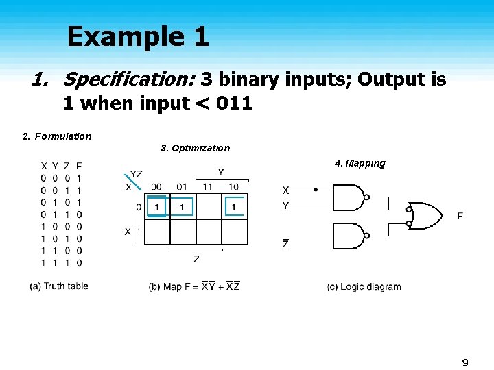
Example 1 1. Specification: 3 binary inputs; Output is 1 when input < 011 2. Formulation 3. Optimization 4. Mapping 9
5. Verification • Verify correctness of design • Manual: perform analysis of circuit • Simulation 10
Analysis of Circuit • Used in manual design verification and other purposes • This shows a disciplined way to analyze a circuit ♦ To get Boolean function ♦ and/or Truth table 11
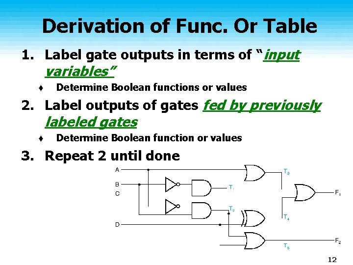
Derivation of Func. Or Table 1. Label gate outputs in terms of “input variables” ♦ Determine Boolean functions or values 2. Label outputs of gates fed by previously labeled gates ♦ Determine Boolean function or values 3. Repeat 2 until done 12
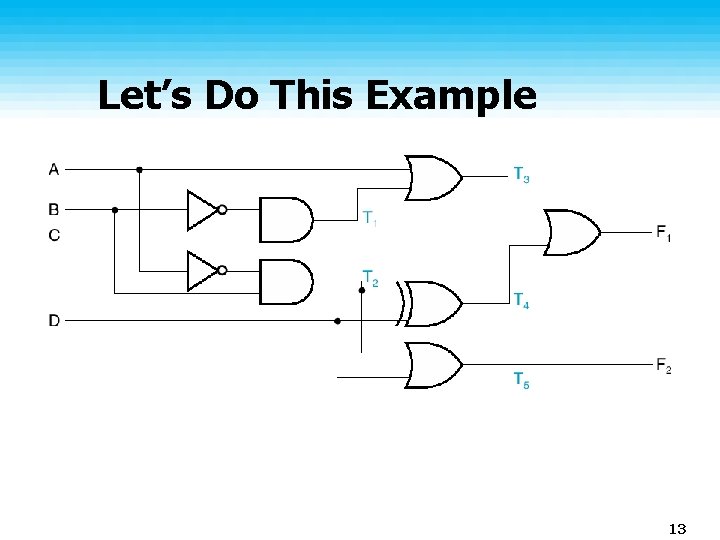
Let’s Do This Example 13
Derivation of Truth Table • Make table with 2 n rows, where n is number of inputs • Label some gate outputs • Put those labels and the final outputs on columns of truth table • Work your way across 14
Design Examples • Design Examples in the book ♦ Study on your own: • Example 3 -1 (p. 99) : Design of a BCD-to-Excess-3 Converter • Example 3 -2 (p. 101) : Design of a BCD-Seven-Segment Decoder • Examples 3 -3 (Will do in class) : Design of a 4 -bit Equality Comparator ♦ Input: 2 vectors A(3: 0) and B(3: 0) ♦ Output: One bit, E, which is 1 if A and B are bitwise equal, 0 otherwise 15
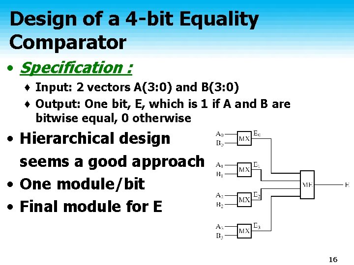
Design of a 4 -bit Equality Comparator • Specification : ♦ Input: 2 vectors A(3: 0) and B(3: 0) ♦ Output: One bit, E, which is 1 if A and B are bitwise equal, 0 otherwise • Hierarchical design seems a good approach • One module/bit • Final module for E 16
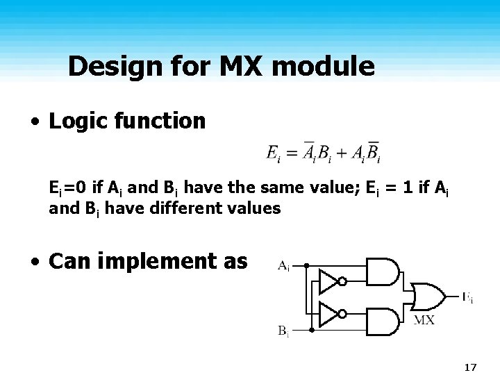
Design for MX module • Logic function Ei=0 if Ai and Bi have the same value; Ei = 1 if Ai and Bi have different values • Can implement as 17
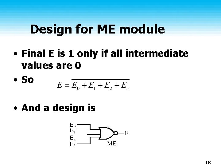
Design for ME module • Final E is 1 only if all intermediate values are 0 • So • And a design is 18
- Slides: 18