Combinational Circuit Design COE 202 Digital Logic Design

Combinational Circuit Design COE 202 Digital Logic Design Dr. Muhamed Mudawar King Fahd University of Petroleum and Minerals
Presentation Outline v How to Design a Combinational Circuit v Designing a BCD to Excess-3 Code Converter v Designing a BCD to 7 -Segment Decoder v Hierarchical Design v Iterative Design Combinational Circuit Design COE 202 – Digital Logic Design © Muhamed Mudawar – slide 2
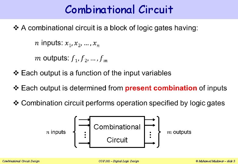
Combinational Circuit v Combinational Circuit Design Circuit COE 202 – Digital Logic Design Combinational © Muhamed Mudawar – slide 3
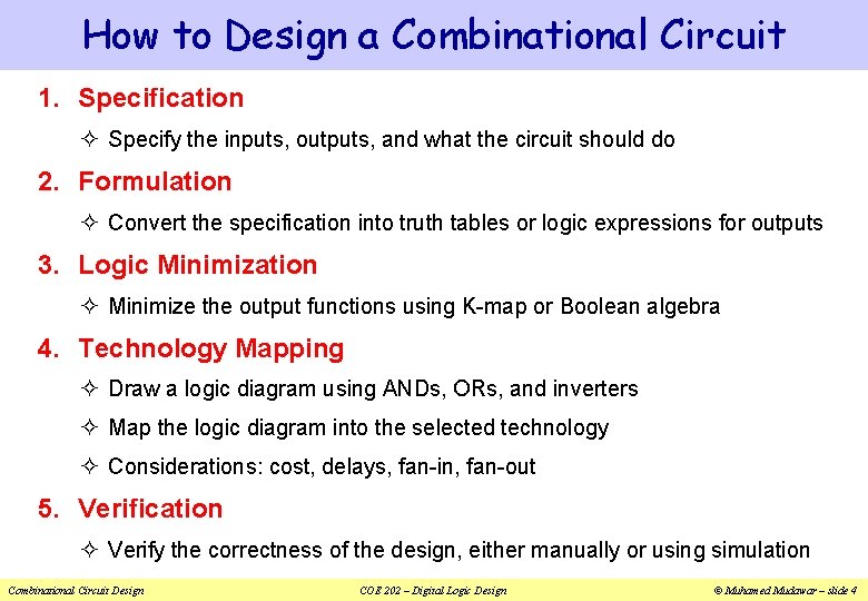
How to Design a Combinational Circuit 1. Specification ² Specify the inputs, outputs, and what the circuit should do 2. Formulation ² Convert the specification into truth tables or logic expressions for outputs 3. Logic Minimization ² Minimize the output functions using K-map or Boolean algebra 4. Technology Mapping ² Draw a logic diagram using ANDs, ORs, and inverters ² Map the logic diagram into the selected technology ² Considerations: cost, delays, fan-in, fan-out 5. Verification ² Verify the correctness of the design, either manually or using simulation Combinational Circuit Design COE 202 – Digital Logic Design © Muhamed Mudawar – slide 4
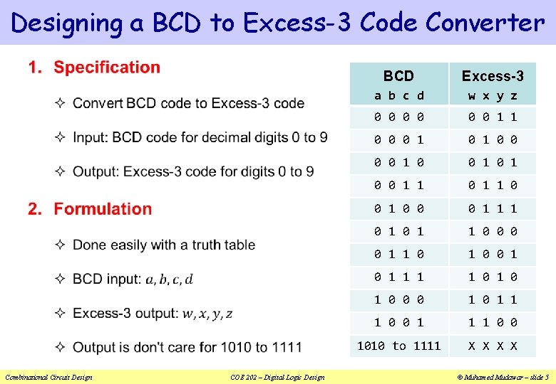
Designing a BCD to Excess-3 Code Converter v Combinational Circuit Design COE 202 – Digital Logic Design BCD Excess-3 a b c d w x y z 0 0 0 1 1 0 0 0 1 0 0 1 1 0 0 0 1 1 1 0 0 1 1 0 0 1 1 1 1 0 1 0 0 0 1 1 1 0 0 1010 to 1111 X X © Muhamed Mudawar – slide 5
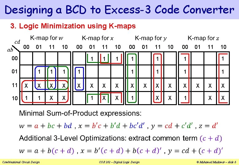
Designing a BCD to Excess-3 Code Converter 3. Logic Minimization using K-maps 00 01 11 10 00 00 01 1 1 X 11 X X 10 1 1 X X Combinational Circuit Design 01 11 10 00 1 1 1 X X 1 COE 202 – Digital Logic Design 01 X 11 10 00 X X X 1 01 X 11 10 X X © Muhamed Mudawar – slide 6
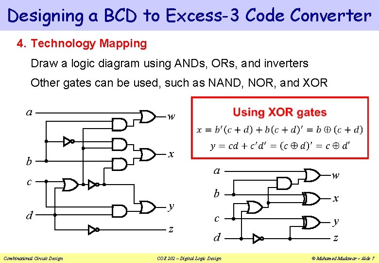
Designing a BCD to Excess-3 Code Converter 4. Technology Mapping Draw a logic diagram using ANDs, ORs, and inverters Other gates can be used, such as NAND, NOR, and XOR a b w x c d y z Combinational Circuit Design a w b x c y z d COE 202 – Digital Logic Design © Muhamed Mudawar – slide 7
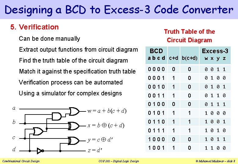
Designing a BCD to Excess-3 Code Converter 5. Verification Truth Table of the Circuit Diagram Can be done manually Extract output functions from circuit diagram BCD Excess-3 Find the truth table of the circuit diagram a b c d c+d b(c+d) w x y z Match it against the specification truth table 0000 0 0 1 1 0001 1 0 0 0010 1 0 1 0011 1 0 0100 0 0 w = a + b(c + d) 0 1 1 1 0101 1 0 0 0 x = b (c + d) 0110 1 1 1 0 0 1 0111 1 0 1 0 c y = c d' 1000 0 0 1 1 d z = d' 1001 1 0 0 Verification process can be automated Using a simulator for complex designs a b Combinational Circuit Design COE 202 – Digital Logic Design © Muhamed Mudawar – slide 8
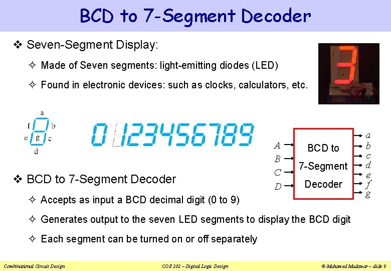
BCD to 7 -Segment Decoder v Seven-Segment Display: ² Made of Seven segments: light-emitting diodes (LED) ² Found in electronic devices: such as clocks, calculators, etc. v BCD to 7 -Segment Decoder A B C D BCD to 7 -Segment Decoder ² Accepts as input a BCD decimal digit (0 to 9) a b c d e f g ² Generates output to the seven LED segments to display the BCD digit ² Each segment can be turned on or off separately Combinational Circuit Design COE 202 – Digital Logic Design © Muhamed Mudawar – slide 9
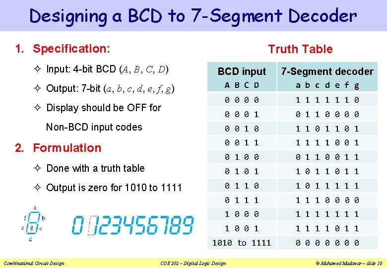
Designing a BCD to 7 -Segment Decoder 1. Specification: Truth Table ² Input: 4 -bit BCD (A, B, C, D) BCD input 7 -Segment decoder A B C D a b c d e f g 0 0 1 1 1 0 0 1 0 1 1 0 0 1 1 1 0 0 0 1 1 ² Done with a truth table 0 1 1 ² Output is zero for 1010 to 1111 0 1 0 1 1 1 0 0 1 0 0 0 1 1 1 1 0 0 1 1 1010 to 1111 0 0 0 0 ² Output: 7 -bit (a, b, c, d, e, f, g) ² Display should be OFF for Non-BCD input codes 2. Formulation Combinational Circuit Design COE 202 – Digital Logic Design © Muhamed Mudawar – slide 10
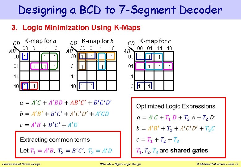
Designing a BCD to 7 -Segment Decoder 3. Logic Minimization Using K-Maps 00 01 11 10 00 1 01 1 1 00 1 1 1 01 1 Combinational Circuit Design 10 1 11 11 10 1 1 1 00 01 11 10 00 1 1 1 01 1 1 11 1 10 1 COE 202 – Digital Logic Design 1 © Muhamed Mudawar – slide 11
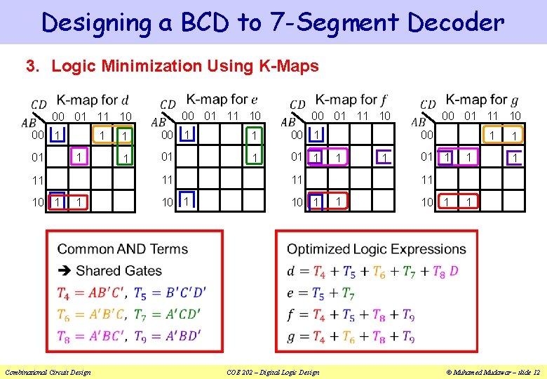
Designing a BCD to 7 -Segment Decoder 3. Logic Minimization Using K-Maps 00 1 01 1 1 11 10 1 1 Combinational Circuit Design 00 01 11 10 1 00 1 1 01 1 11 11 10 1 COE 202 – Digital Logic Design 00 01 11 10 00 1 1 1 01 1 1 11 1 10 1 1 © Muhamed Mudawar – slide 12
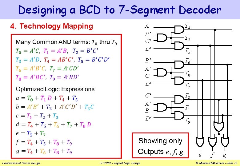
Designing a BCD to 7 -Segment Decoder 4. Technology Mapping A B' C' D' T 4 B' A' C D' T 6 C' A' B D' T 8 Showing only Outputs e, f, g Combinational Circuit Design COE 202 – Digital Logic Design T 2 T 5 T 0 T 7 T 1 T 9 e f g © Muhamed Mudawar – slide 13
Verification Methods v Manual Logic Analysis ² Find the logic expressions and truth table of the final circuit ² Compare the final circuit truth table against the specified truth table ² Compare the circuit output expressions against the specified expressions ² Tedious for large designs + Human Errors v Simulation ² Simulate the final circuit, possibly written in HDL (such as Verilog) ² Write a test bench that automates the verification process ² Generate test cases for ALL possible inputs (exhaustive testing) ² Verify the output correctness for ALL input test cases ² Exhaustive testing can be very time consuming for many inputs Combinational Circuit Design COE 202 – Digital Logic Design © Muhamed Mudawar – slide 14
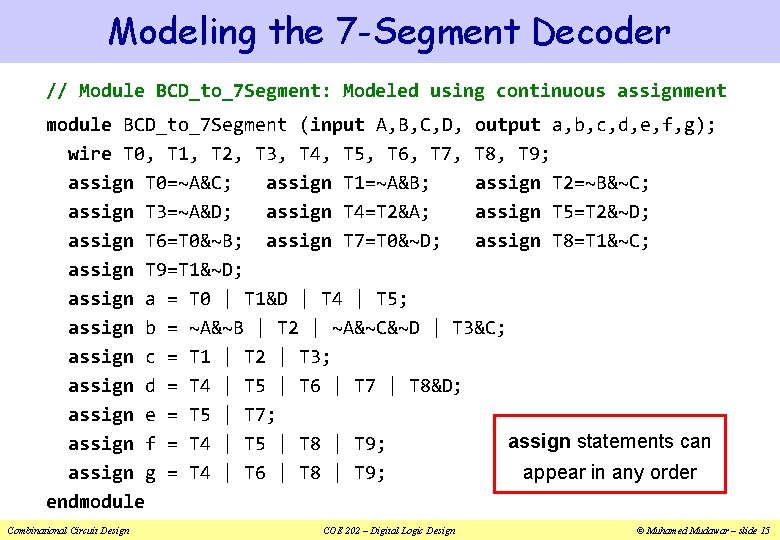
Modeling the 7 -Segment Decoder // Module BCD_to_7 Segment: Modeled using continuous assignment module BCD_to_7 Segment (input A, B, C, D, output a, b, c, d, e, f, g); wire T 0, T 1, T 2, T 3, T 4, T 5, T 6, T 7, T 8, T 9; assign T 0=~A&C; assign T 1=~A&B; assign T 2=~B&~C; assign T 3=~A&D; assign T 4=T 2&A; assign T 5=T 2&~D; assign T 6=T 0&~B; assign T 7=T 0&~D; assign T 8=T 1&~C; assign T 9=T 1&~D; assign a = T 0 | T 1&D | T 4 | T 5; assign b = ~A&~B | T 2 | ~A&~C&~D | T 3&C; assign c = T 1 | T 2 | T 3; assign d = T 4 | T 5 | T 6 | T 7 | T 8&D; assign e = T 5 | T 7; assign statements can assign f = T 4 | T 5 | T 8 | T 9; appear in any order assign g = T 4 | T 6 | T 8 | T 9; endmodule Combinational Circuit Design COE 202 – Digital Logic Design © Muhamed Mudawar – slide 15
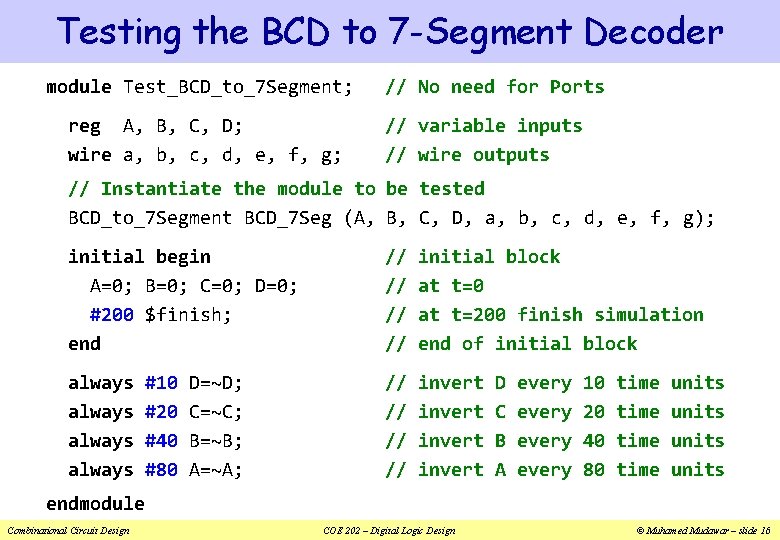
Testing the BCD to 7 -Segment Decoder module Test_BCD_to_7 Segment; reg A, B, C, D; wire a, b, c, d, e, f, g; // No need for Ports // variable inputs // wire outputs // Instantiate the module to be tested BCD_to_7 Segment BCD_7 Seg (A, B, C, D, a, b, c, d, e, f, g); initial begin A=0; B=0; C=0; D=0; #200 $finish; end // // initial block at t=0 at t=200 finish simulation end of initial block always // // invert #10 #20 #40 #80 D=~D; C=~C; B=~B; A=~A; D C B A every 10 20 40 80 time units endmodule Combinational Circuit Design COE 202 – Digital Logic Design © Muhamed Mudawar – slide 16
The initial and always Blocks v There are two types of procedural blocks in Verilog 1. The initial block ² Executes the enclosed statement(s) once 2. The always block ² Executes the enclosed statement(s) repeatedly until simulation terminates v The body of the initial and always blocks is procedural ² Can enclose one or more procedural statements ² Procedural statements surrounded by begin … end execute sequentially ² #delay is used to delay the execution of the procedural statement v Procedural blocks can appear in any order inside a module v Multiple procedural blocks run in parallel inside the simulator Combinational Circuit Design COE 202 – Digital Logic Design © Muhamed Mudawar – slide 17
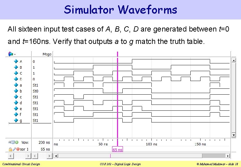
Simulator Waveforms All sixteen input test cases of A, B, C, D are generated between t=0 and t=160 ns. Verify that outputs a to g match the truth table. Combinational Circuit Design COE 202 – Digital Logic Design © Muhamed Mudawar – slide 18
Hierarchical Design v Why Hierarchical Design? To simplify the implementation of a complex circuit v What is Hierarchical Design? Decompose a complex circuit into smaller pieces called blocks Decompose each block into even smaller blocks Repeat as necessary until the blocks are small enough Any block not decomposed is called a primitive block The hierarchy is a tree of blocks at different levels v The blocks are verified and well-document v They are placed in a library for future use Combinational Circuit Design COE 202 – Digital Logic Design © Muhamed Mudawar – slide 19
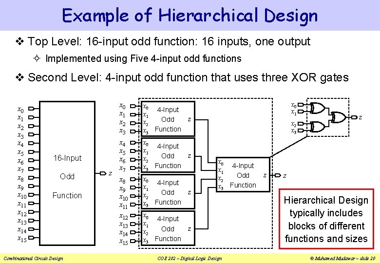
Example of Hierarchical Design v Top Level: 16 -input odd function: 16 inputs, one output ² Implemented using Five 4 -input odd functions v Second Level: 4 -input odd function that uses three XOR gates x 0 x 1 x 2 x 3 x 4 x 5 x 6 x 7 x 8 x 9 x 10 x 11 x 12 x 13 x 14 x 15 16 -Input Odd Function Combinational Circuit Design z x 0 x 1 x 2 x 3 x 0 4 -Input x 1 Odd x 2 x 3 Function z x 4 x 5 x 6 x 7 x 0 4 -Input x 1 Odd x 2 x 3 Function z x 8 x 9 x 10 x 11 x 12 x 13 x 14 x 15 x 0 4 -Input x 1 Odd x 2 x 3 Function z x 0 x 1 x 2 x 3 x 0 4 -Input x 1 Odd x 2 x 3 Function COE 202 – Digital Logic Design z z z Hierarchical Design typically includes blocks of different functions and sizes © Muhamed Mudawar – slide 20
Top-Down versus Bottom-Up Design v A top-down design proceeds from a high-level specification to a more and more detailed design by decomposition and successive refinement v A bottom-up design starts with detailed primitive blocks and combines them into larger and more complex functional blocks v Design usually proceeds top-down to a known set of building blocks, ranging from complete processors to primitive logic gates Combinational Circuit Design COE 202 – Digital Logic Design © Muhamed Mudawar – slide 21
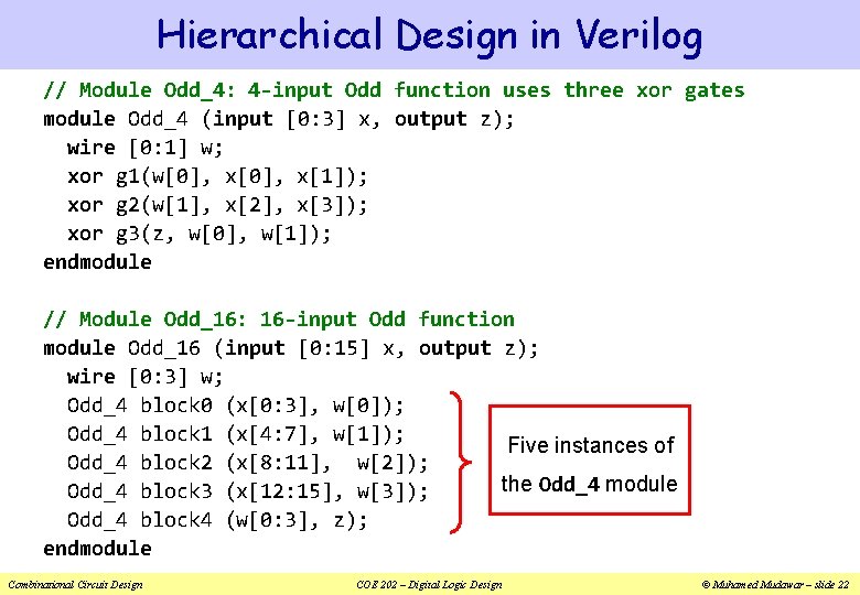
Hierarchical Design in Verilog // Module Odd_4: 4 -input Odd function uses three xor gates module Odd_4 (input [0: 3] x, output z); wire [0: 1] w; xor g 1(w[0], x[1]); xor g 2(w[1], x[2], x[3]); xor g 3(z, w[0], w[1]); endmodule // Module Odd_16: 16 -input Odd function module Odd_16 (input [0: 15] x, output z); wire [0: 3] w; Odd_4 block 0 (x[0: 3], w[0]); Odd_4 block 1 (x[4: 7], w[1]); Five instances of Odd_4 block 2 (x[8: 11], w[2]); the Odd_4 module Odd_4 block 3 (x[12: 15], w[3]); Odd_4 block 4 (w[0: 3], z); endmodule Combinational Circuit Design COE 202 – Digital Logic Design © Muhamed Mudawar – slide 22
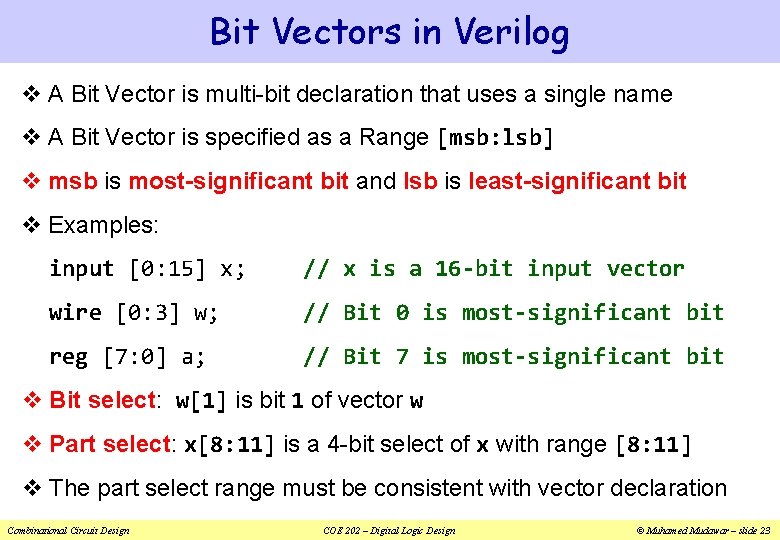
Bit Vectors in Verilog v A Bit Vector is multi-bit declaration that uses a single name v A Bit Vector is specified as a Range [msb: lsb] v msb is most-significant bit and lsb is least-significant bit v Examples: input [0: 15] x; // x is a 16 -bit input vector wire [0: 3] w; // Bit 0 is most-significant bit reg [7: 0] a; // Bit 7 is most-significant bit v Bit select: w[1] is bit 1 of vector w v Part select: x[8: 11] is a 4 -bit select of x with range [8: 11] v The part select range must be consistent with vector declaration Combinational Circuit Design COE 202 – Digital Logic Design © Muhamed Mudawar – slide 23
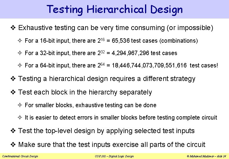
Testing Hierarchical Design v Exhaustive testing can be very time consuming (or impossible) ² For a 16 -bit input, there are 216 = 65, 536 test cases (combinations) ² For a 32 -bit input, there are 232 = 4, 294, 967, 296 test cases ² For a 64 -bit input, there are 264 = 18, 446, 744, 073, 709, 551, 616 test cases! v Testing a hierarchical design requires a different strategy v Test each block in the hierarchy separately ² For smaller blocks, exhaustive testing can be done ² It is easier to detect errors in smaller blocks before testing complete circuit v Test the top-level design by applying selected test inputs v Make sure that the test inputs exercise all parts of the circuit Combinational Circuit Design COE 202 – Digital Logic Design © Muhamed Mudawar – slide 24
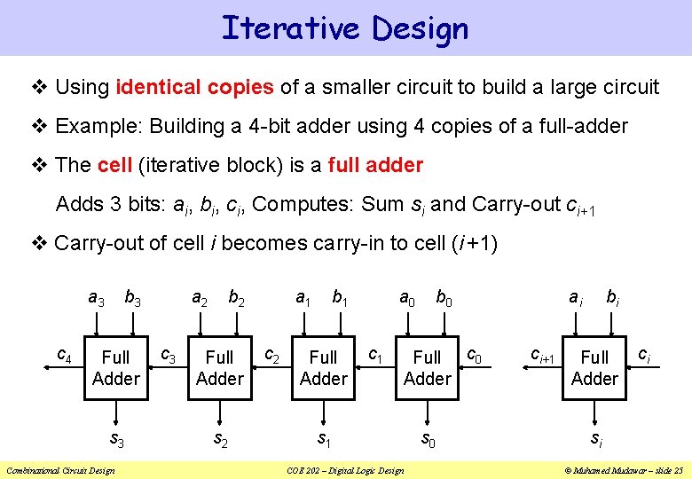
Iterative Design v Using identical copies of a smaller circuit to build a large circuit v Example: Building a 4 -bit adder using 4 copies of a full-adder v The cell (iterative block) is a full adder Adds 3 bits: ai, bi, ci, Computes: Sum si and Carry-out ci+1 v Carry-out of cell i becomes carry-in to cell (i +1) a 3 c 4 b 3 Full Adder s 3 Combinational Circuit Design a 2 c 3 b 2 Full Adder s 2 a 1 c 2 b 1 Full Adder a 0 c 1 s 1 COE 202 – Digital Logic Design b 0 Full c 0 Adder s 0 ai ci+1 bi Full Adder ci si © Muhamed Mudawar – slide 25
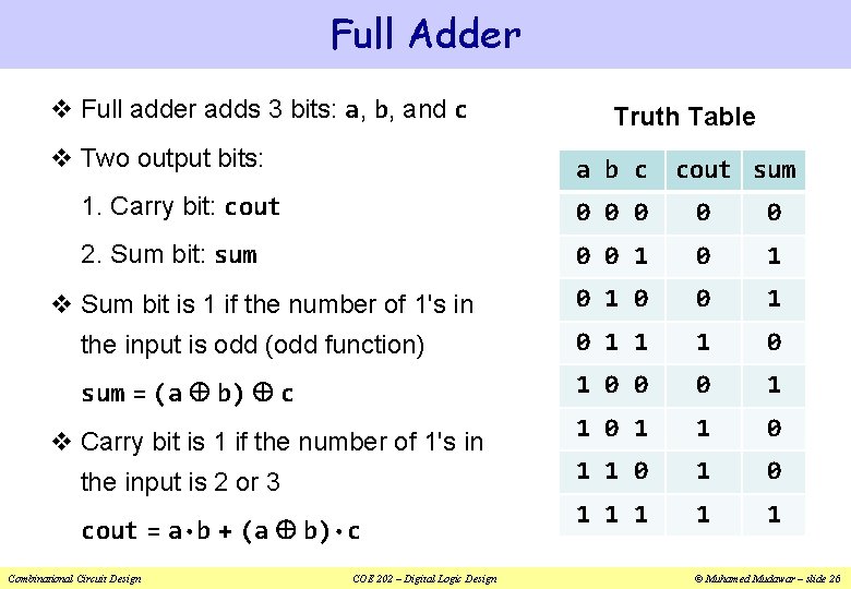
Full Adder v Full adder adds 3 bits: a, b, and c v Two output bits: Truth Table a b c cout sum 1. Carry bit: cout 0 0 0 2. Sum bit: sum 0 0 1 0 1 0 0 1 the input is odd (odd function) 0 1 1 1 0 sum = (a b) c 1 0 0 0 1 1 0 1 1 1 v Sum bit is 1 if the number of 1's in v Carry bit is 1 if the number of 1's in the input is 2 or 3 cout = a·b + (a b)·c Combinational Circuit Design COE 202 – Digital Logic Design © Muhamed Mudawar – slide 26
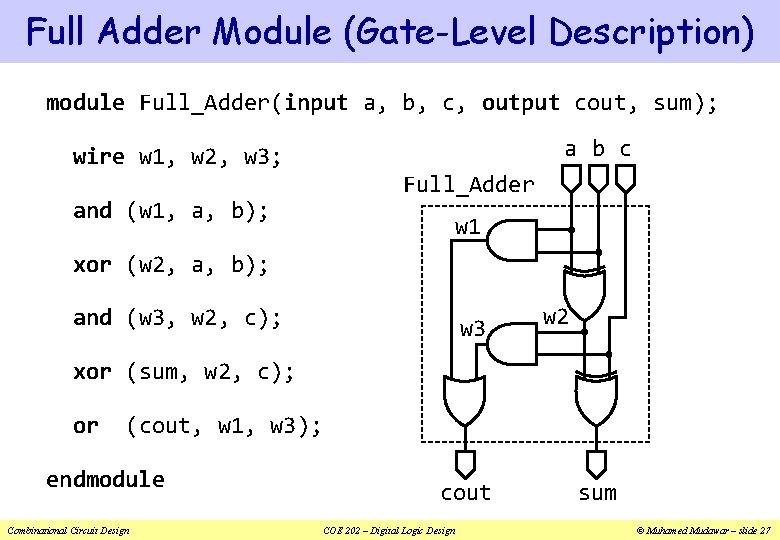
Full Adder Module (Gate-Level Description) module Full_Adder(input a, b, c, output cout, sum); a b c wire w 1, w 2, w 3; Full_Adder and (w 1, a, b); w 1 xor (w 2, a, b); and (w 3, w 2, c); w 3 w 2 xor (sum, w 2, c); or (cout, w 1, w 3); endmodule Combinational Circuit Design cout COE 202 – Digital Logic Design sum © Muhamed Mudawar – slide 27
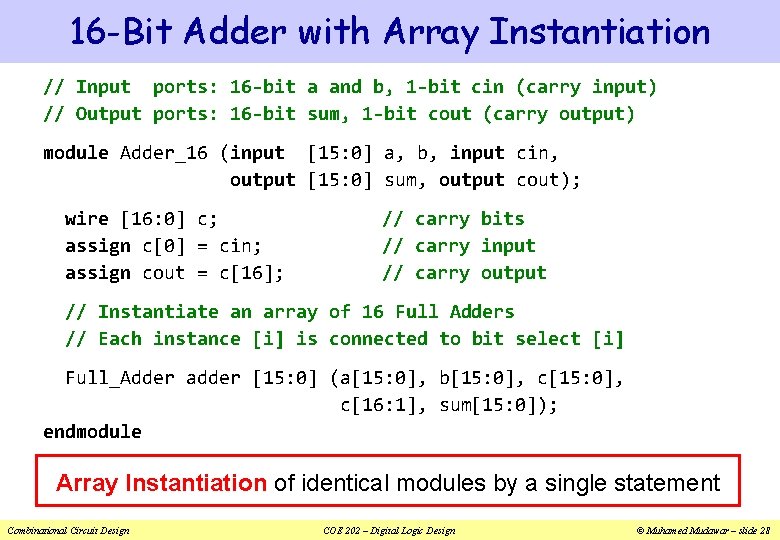
16 -Bit Adder with Array Instantiation // Input ports: 16 -bit a and b, 1 -bit cin (carry input) // Output ports: 16 -bit sum, 1 -bit cout (carry output) module Adder_16 (input [15: 0] a, b, input cin, output [15: 0] sum, output cout); wire [16: 0] c; assign c[0] = cin; assign cout = c[16]; // carry bits // carry input // carry output // Instantiate an array of 16 Full Adders // Each instance [i] is connected to bit select [i] Full_Adder adder [15: 0] (a[15: 0], b[15: 0], c[16: 1], sum[15: 0]); endmodule Array Instantiation of identical modules by a single statement Combinational Circuit Design COE 202 – Digital Logic Design © Muhamed Mudawar – slide 28
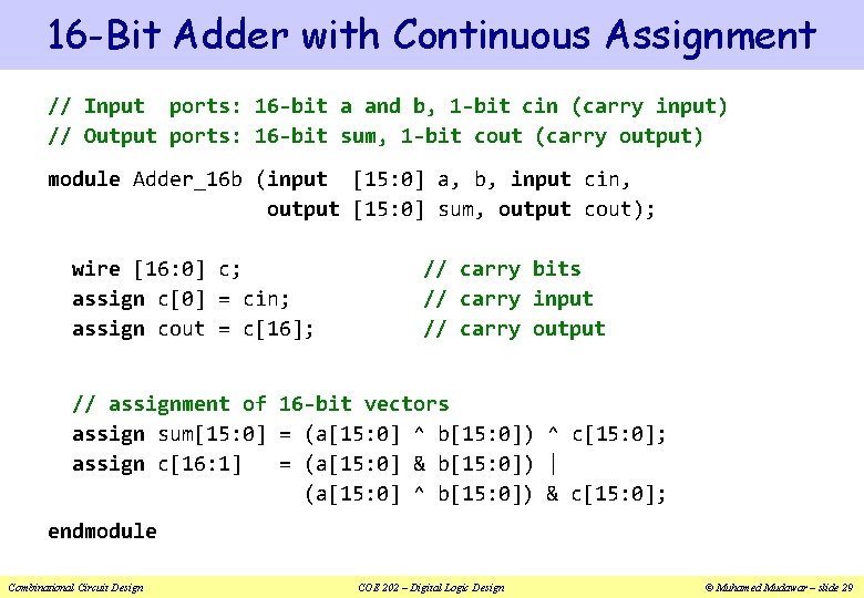
16 -Bit Adder with Continuous Assignment // Input ports: 16 -bit a and b, 1 -bit cin (carry input) // Output ports: 16 -bit sum, 1 -bit cout (carry output) module Adder_16 b (input [15: 0] a, b, input cin, output [15: 0] sum, output cout); wire [16: 0] c; assign c[0] = cin; assign cout = c[16]; // carry bits // carry input // carry output // assignment of 16 -bit vectors assign sum[15: 0] = (a[15: 0] ^ b[15: 0]) ^ c[15: 0]; assign c[16: 1] = (a[15: 0] & b[15: 0]) | (a[15: 0] ^ b[15: 0]) & c[15: 0]; endmodule Combinational Circuit Design COE 202 – Digital Logic Design © Muhamed Mudawar – slide 29
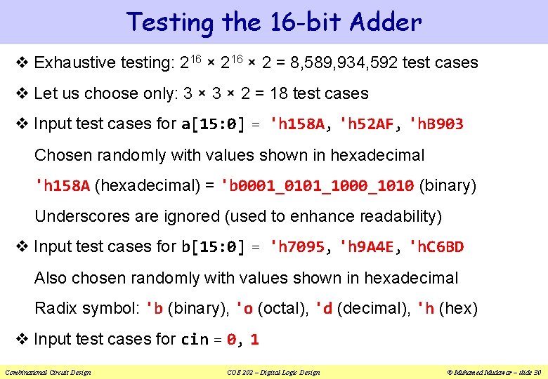
Testing the 16 -bit Adder v Exhaustive testing: 216 × 2 = 8, 589, 934, 592 test cases v Let us choose only: 3 × 2 = 18 test cases v Input test cases for a[15: 0] = 'h 158 A, 'h 52 AF, 'h. B 903 Chosen randomly with values shown in hexadecimal 'h 158 A (hexadecimal) = 'b 0001_0101_1000_1010 (binary) Underscores are ignored (used to enhance readability) v Input test cases for b[15: 0] = 'h 7095, 'h 9 A 4 E, 'h. C 6 BD Also chosen randomly with values shown in hexadecimal Radix symbol: 'b (binary), 'o (octal), 'd (decimal), 'h (hex) v Input test cases for cin = 0, 1 Combinational Circuit Design COE 202 – Digital Logic Design © Muhamed Mudawar – slide 30
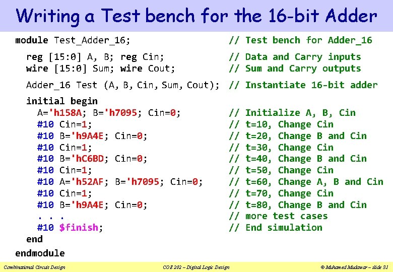
Writing a Test bench for the 16 -bit Adder module Test_Adder_16; // Test bench for Adder_16 reg [15: 0] A, B; reg Cin; wire [15: 0] Sum; wire Cout; // Data and Carry inputs // Sum and Carry outputs Adder_16 Test (A, B, Cin, Sum, Cout); // Instantiate 16 -bit adder initial begin A='h 158 A; B='h 7095; Cin=0; #10 Cin=1; #10 B='h 9 A 4 E; Cin=0; #10 Cin=1; #10 B='h. C 6 BD; Cin=0; #10 Cin=1; #10 A='h 52 AF; B='h 7095; Cin=0; #10 Cin=1; #10 B='h 9 A 4 E; Cin=0; . . . #10 $finish; endmodule Combinational Circuit Design // // // COE 202 – Digital Logic Design Initialize A, B, Cin t=10, Change Cin t=20, Change B and Cin t=30, Change Cin t=40, Change B and Cin t=50, Change Cin t=60, Change A, B and Cin t=70, Change Cin t=80, Change B and Cin more test cases End simulation © Muhamed Mudawar – slide 31
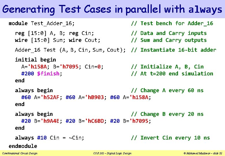
Generating Test Cases in parallel with always module Test_Adder_16; // Test bench for Adder_16 reg [15: 0] A, B; reg Cin; wire [15: 0] Sum; wire Cout; // Data and Carry inputs // Sum and Carry outputs Adder_16 Test (A, B, Cin, Sum, Cout); // Instantiate 16 -bit adder initial begin A='h 158 A; B='h 7095; Cin=0; #200 $finish; end // Initialize A, B, Cin // At t=200 end simulation always begin // Change A every 60 ns #60 A='h 52 AF; #60 A='h. B 903; #60 A='h 158 A; end always begin // Change B every 20 ns #20 B='h 9 A 4 E; #20 B='h. C 6 BD; #20 B='h 7095; end always #10 Cin = ~Cin; endmodule Combinational Circuit Design // Invert Cin every 10 ns COE 202 – Digital Logic Design © Muhamed Mudawar – slide 32
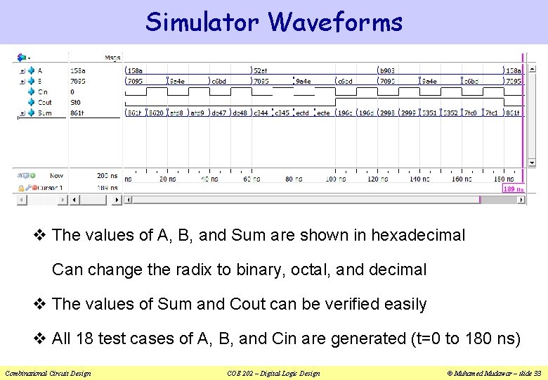
Simulator Waveforms v The values of A, B, and Sum are shown in hexadecimal Can change the radix to binary, octal, and decimal v The values of Sum and Cout can be verified easily v All 18 test cases of A, B, and Cin are generated (t=0 to 180 ns) Combinational Circuit Design COE 202 – Digital Logic Design © Muhamed Mudawar – slide 33
- Slides: 33