COLDADC Schedule David Christian COLDADC Redesign Team Redesign
- Slides: 6

COLDADC Schedule David Christian

COLDADC Redesign Team • Redesign will be done mostly by the same designers responsible for the first prototype. • General Responsibilities: 2 • BNL: Input Buffers, Bandgap Reference Block, Digital Synthesis & Pn. R (Sandeep Miryala is now at BNL) • LBL: SHA, MUX, & pipeline ADCs • Fermilab: Digital backend logic, Power On Reset, pad ring, final integration and verification. Feb. 5, 2020 David Christian | COLDADC Schedule

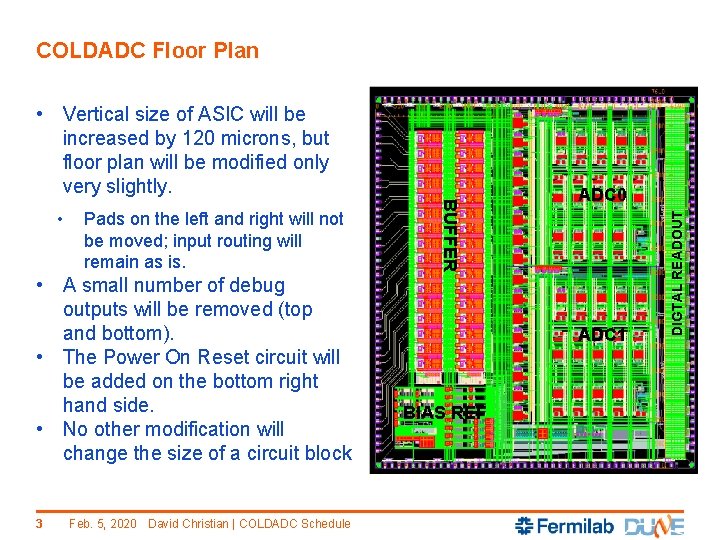
COLDADC Floor Plan Pads on the left and right will not be moved; input routing will remain as is. • A small number of debug outputs will be removed (top and bottom). • The Power On Reset circuit will be added on the bottom right hand side. • No other modification will change the size of a circuit block 3 Feb. 5, 2020 David Christian | COLDADC Schedule BUFFER • ADC 0 ADC 1 BIAS REF DIGTAL READOUT • Vertical size of ASIC will be increased by 120 microns, but floor plan will be modified only very slightly.

Status • BNL • 4 • Input buffers are done. • Bandgap reference fix is understood, simulated at the schematic level, layout still needs modification. • RTL synthesis & Pn. R can start now. LBL • Changes in digital logic (autocalibration & overrange protection) are understood, RTL modification is next. • After RTL synthesis & Pn. R, LBL will place digital logic into analog block(s) • Pipeline ADC: design of improved Op. Amp is done; layout and post-layout simulation is next. • Changes to MUX are minor; layout is next. • Last step before full-chip integration is mixed-mode simulation including layout parasitics. Feb. 5, 2020 David Christian | COLDADC Schedule

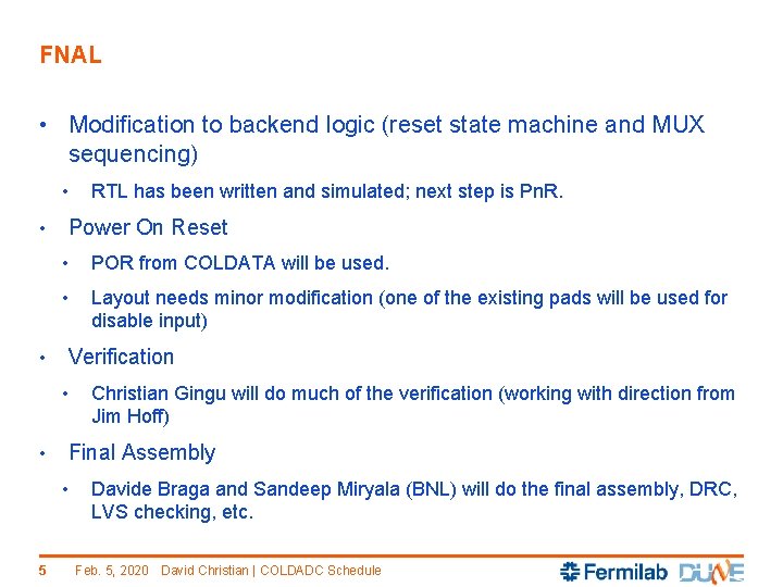
FNAL • Modification to backend logic (reset state machine and MUX sequencing) • • • Power On Reset • POR from COLDATA will be used. • Layout needs minor modification (one of the existing pads will be used for disable input) Verification • • Christian Gingu will do much of the verification (working with direction from Jim Hoff) Final Assembly • 5 RTL has been written and simulated; next step is Pn. R. Davide Braga and Sandeep Miryala (BNL) will do the final assembly, DRC, LVS checking, etc. Feb. 5, 2020 David Christian | COLDADC Schedule

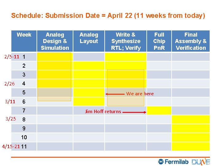
Schedule: Submission Date = April 22 (11 weeks from today) Week Analog Design & Simulation Analog Layout Write & Synthesize RTL; Verify Full Chip Pn. R 2/5 -11 1 2 3 2/26 4 5 3/11 6 7 3/25 We are here 8 9 10 4/15 -21 11 Jim Hoff returns Final Assembly & Verification