
Cold Cathode Development for Electron Coolers BRUNO GALANTE
Cold Cathode Development for Electron Coolers BRUNO GALANTE BE-BI-EA BI DAY 04 -12 -2018 BI Day - 04/12/2018 BRUNO. GALANTE@CERN. CH 1
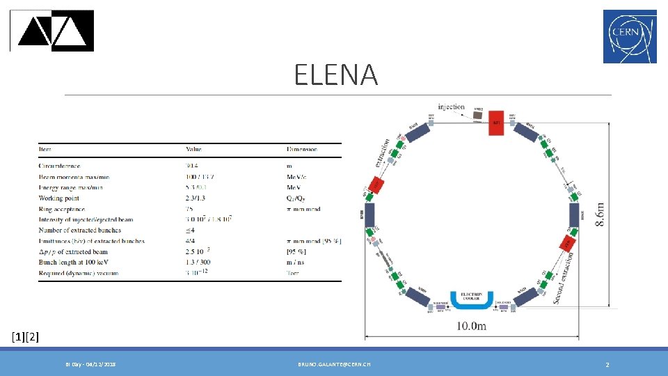
ELENA [1][2] BI Day - 04/12/2018 BRUNO. GALANTE@CERN. CH 2
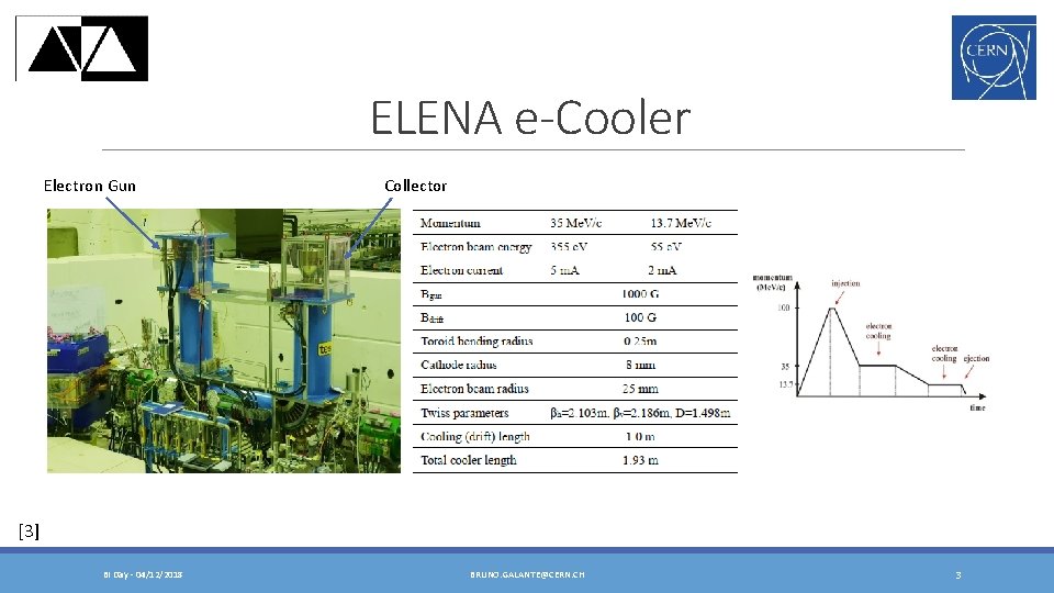
ELENA e-Cooler Electron Gun Collector [3] BI Day - 04/12/2018 BRUNO. GALANTE@CERN. CH 3
Electron Gun It must produce a • Cold (T⊥ < 0. 1 e. V, T// < 1 me. V) • Intense electron beam (ne ≈ 1. 5 x 1012 cm-3) Thermionic cathodes limit the performance of electron cooling due to high T of the emitted beam while photocathodes suffer of an usually quite low lifetime. Alternative solution: Field Emission due to have a Cold Cathode. BI Day - 04/12/2018 BRUNO. GALANTE@CERN. CH 4
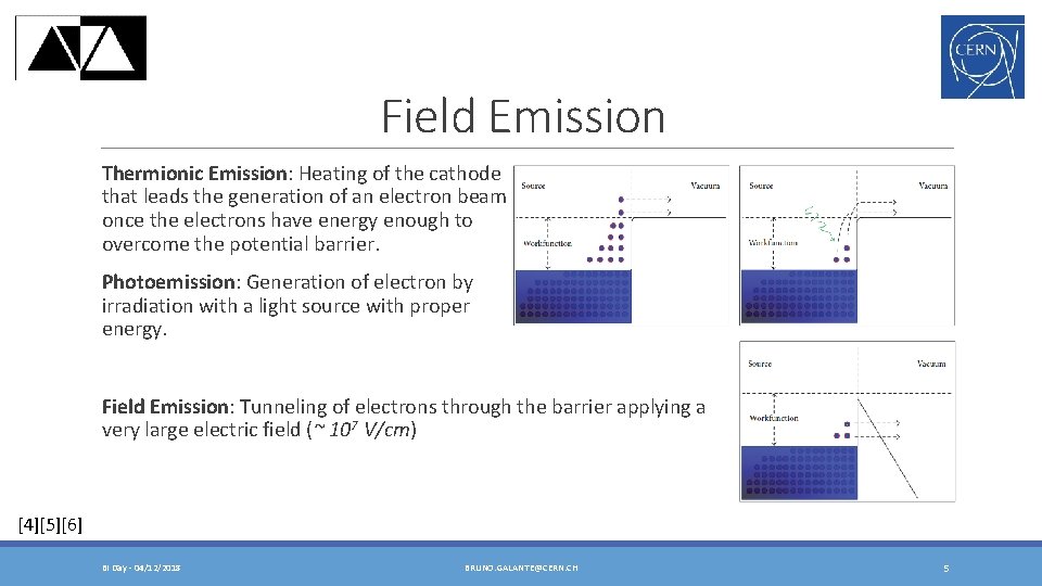
Field Emission Thermionic Emission: Heating of the cathode that leads the generation of an electron beam once the electrons have energy enough to overcome the potential barrier. Photoemission: Generation of electron by irradiation with a light source with proper energy. Field Emission: Tunneling of electrons through the barrier applying a very large electric field (~ 107 V/cm) [4][5][6] BI Day - 04/12/2018 BRUNO. GALANTE@CERN. CH 5
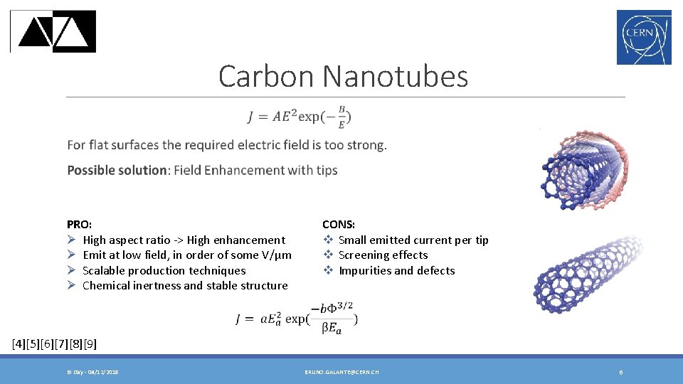
Carbon Nanotubes PRO: Ø High aspect ratio -> High enhancement Ø Emit at low field, in order of some V/μm Ø Scalable production techniques Ø Chemical inertness and stable structure CONS: v Small emitted current per tip v Screening effects v Impurities and defects [4][5][6][7][8][9] BI Day - 04/12/2018 BRUNO. GALANTE@CERN. CH 6
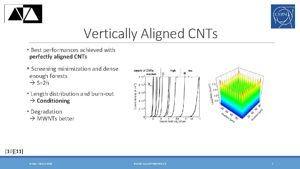
Vertically Aligned CNTs • Best performances achieved with perfectly aligned CNTs • Screening minimization and dense enough forests S=2 h • Length distribution and burn-out Conditioning • Degradation MWNTs better [10][11] BI Day - 04/12/2018 BRUNO. GALANTE@CERN. CH 7
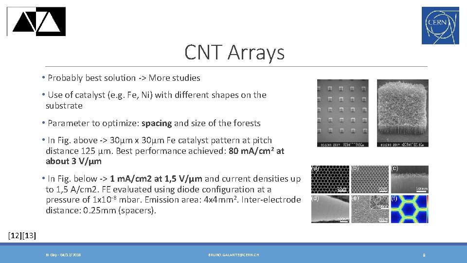
CNT Arrays • Probably best solution -> More studies • Use of catalyst (e. g. Fe, Ni) with different shapes on the substrate • Parameter to optimize: spacing and size of the forests • In Fig. above -> 30µm x 30µm Fe catalyst pattern at pitch distance 125 µm. Best performance achieved: 80 m. A/cm 2 at about 3 V/µm • In Fig. below -> 1 m. A/cm 2 at 1, 5 V/µm and current densities up to 1, 5 A/cm 2. FE evaluated using diode configuration at a pressure of 1 x 10 -8 mbar. Emission area: 4 x 4 mm 2. Inter-electrode distance: 0. 25 mm (spacers). [12][13] BI Day - 04/12/2018 BRUNO. GALANTE@CERN. CH 8
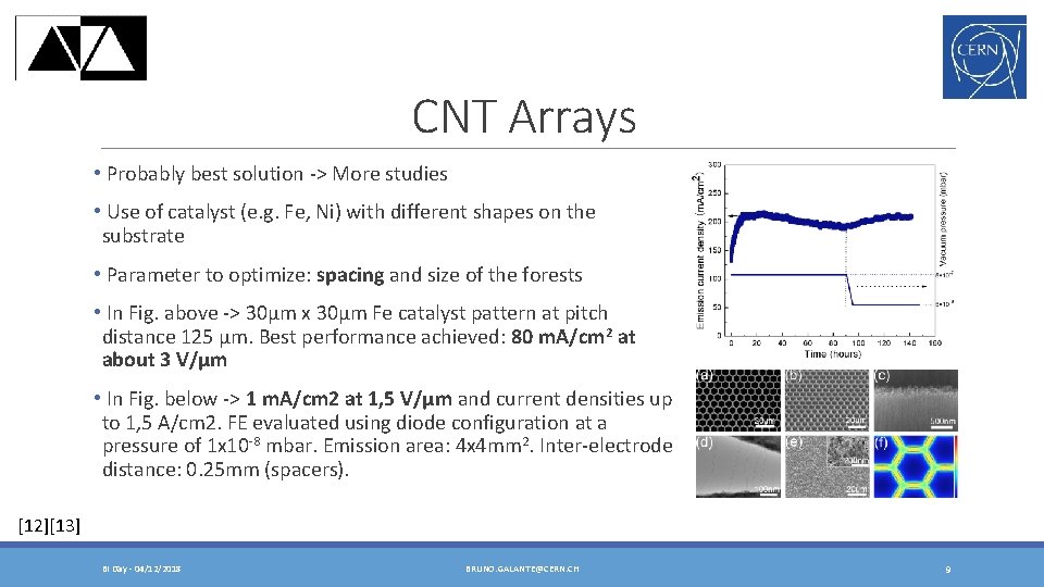
CNT Arrays • Probably best solution -> More studies • Use of catalyst (e. g. Fe, Ni) with different shapes on the substrate • Parameter to optimize: spacing and size of the forests • In Fig. above -> 30µm x 30µm Fe catalyst pattern at pitch distance 125 µm. Best performance achieved: 80 m. A/cm 2 at about 3 V/µm • In Fig. below -> 1 m. A/cm 2 at 1, 5 V/µm and current densities up to 1, 5 A/cm 2. FE evaluated using diode configuration at a pressure of 1 x 10 -8 mbar. Emission area: 4 x 4 mm 2. Inter-electrode distance: 0. 25 mm (spacers). [12][13] BI Day - 04/12/2018 BRUNO. GALANTE@CERN. CH 9
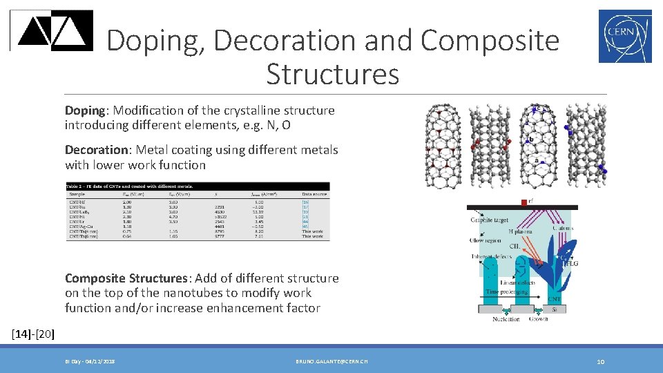
Doping, Decoration and Composite Structures Doping: Modification of the crystalline structure introducing different elements, e. g. N, O Decoration: Metal coating using different metals with lower work function Composite Structures: Add of different structure on the top of the nanotubes to modify work function and/or increase enhancement factor [14]-[20] BI Day - 04/12/2018 BRUNO. GALANTE@CERN. CH 10

Cold Cathode Test Bench Alumina Spacer Substrate + CNT Array BI Day - 04/12/2018 BRUNO. GALANTE@CERN. CH Copper Anode Vespel Insulator Copper foil 11
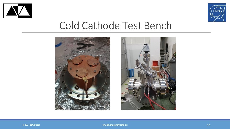
Cold Cathode Test Bench BI Day - 04/12/2018 BRUNO. GALANTE@CERN. CH 12
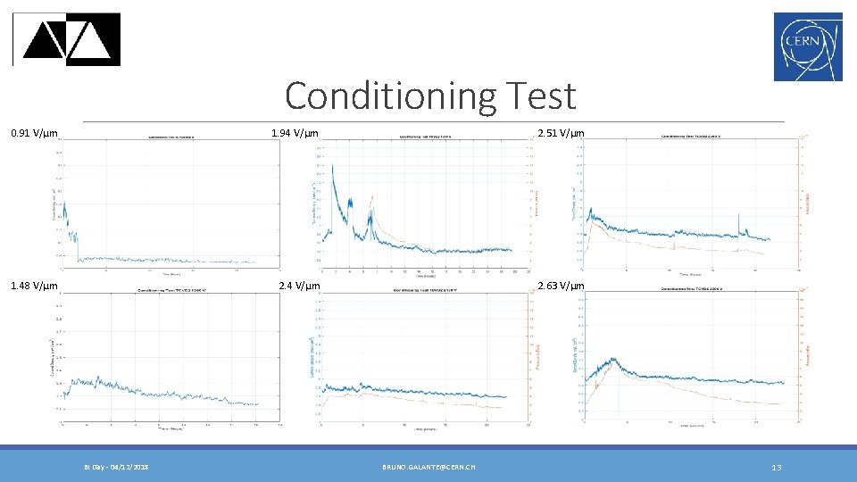
Conditioning Test 0. 91 V/µm 1. 94 V/µm 2. 51 V/µm 1. 48 V/µm 2. 4 V/µm 2. 63 V/µm BI Day - 04/12/2018 BRUNO. GALANTE@CERN. CH 13
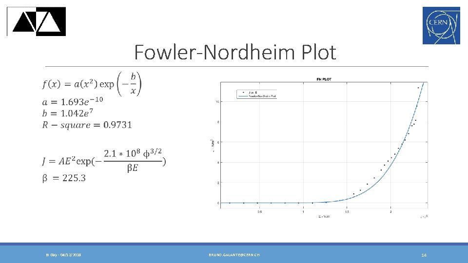
Fowler-Nordheim Plot BI Day - 04/12/2018 BRUNO. GALANTE@CERN. CH 14
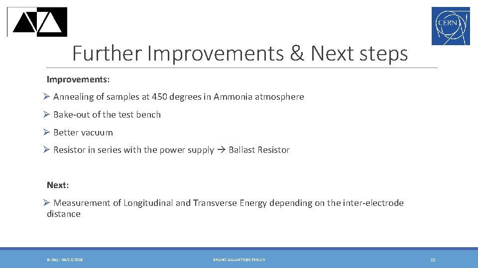
Further Improvements & Next steps Improvements: Ø Annealing of samples at 450 degrees in Ammonia atmosphere Ø Bake-out of the test bench Ø Better vacuum Ø Resistor in series with the power supply Ballast Resistor Next: Ø Measurement of Longitudinal and Transverse Energy depending on the inter-electrode distance BI Day - 04/12/2018 BRUNO. GALANTE@CERN. CH 15
Thank you “AVA has received funding from the European Union’s Horizon 2020 research and innovation programme under the Marie Skłodowska-Curie grant agreement No 721559. ” BI Day - 04/12/2018 BRUNO. GALANTE@CERN. CH 16
References [1] - https: //espace. cern. ch/elena-project/Site. Pages/Home. aspx [2] - ELENA: the extra low energy anti-proton facility at CERN – S. Maury, W. Oelert, W. Bartmann, P. Belochitskii, H. Breuker, F. Butin, C. Carli, T. Eriksson, S. Pasinelli, G. Tranquille [3] - The ELENA electron cooler: parameter choice and expected performance – G. Tranquille, A. Frassier, L. Joergensen [4] - Electron emission in intense electric fields – R. H. Fowler, Dr. L. Nordheim [5] - Carbon Nanotube Electron Source: from electron beams to energy conversion and optophotonics – Alireza Nojeh [6] - Electron field emission from carbon nanotubes – Y. Cheng, O. Zhou [7] - Vacuum nanoelectronics devices: Novel electron sources and applications – A. Evtukh, H. Hartnagel, O. Yilmazoglu, H. Mimura, D. Pavlidis [8] - Carbon nanotubes for cold electron sources – P. Groning, P. Ruffiex, L. Schlapbach, O. Groning [9] - Carbon Nanotube and related field emitters: Fundamentals and applications – Yahachi Saito [10] - Array geometry, size and spacing effects on field emission characteristics of aligned carbon nanotubes – Y. M. Wong, W. P. Kang, J. L. Davidson, B. K. Choi, [11] - Maximizing the electron field emission performance of carbon nanotube arrays – R. C. Smith, S. R. P. Silva [12] - Patterned selective growth of carbon nanotubes and large field emission from vertically well-aligned carbon nanotube field emitter arrays – J. Sohn, S. Lee, Y. -H. Song, S. -Y. Choi, K. -S. Nam [13] - High emission current density, vertically aligned carbon nanotube mesh, field emitter array – C. Li, Y. Zhang, M. Mann, D. Hasko, W. Lei, B. Wang, D. Chu, D. Pribat, G. Amaratunga, W. I. Milne [14] - The doping of carbon nanotubes with nitrogen and their potential applications – P. Ayala, R. Arenal, M. Rummeli, A. Rubio, T. Pichler [15] - Oxygen and nitrogen doping in single wal carbon nanotubes: An efficient stable field emitter – A. Kumar, S. Parveen, S. Husain, M. Zulfequar, Harsh, M. Husain [16] - Improved field emission properties of carbon nanotubes decorated with Ta layer – Z. Wang, Y. Zuo, Y. Li, X. Han, X. Guo, J. Wang, B. Cao, L. Xi, D. Xue BI Day - 04/12/2018 BRUNO. GALANTE@CERN. CH 17
References [17] - Highly improved field emission from vertical graphene-carbon nanotube composites – J. -H. Deng, R. -N. Liu, Y. Zang, W. -X. Zhu, AL. Han, G. -A. Cheng [18] - Highly improved field emission from vertical graphene-carbon nanotube composites – J. -H. Deng, R. -N. Liu, Y. Zang, W. -X. Zhu, AL. Han, G. -A. Cheng [19] - Enhanced field emission properties of a reduced graphene oxide/carbon nanotube hybrid film – D. D. Nguyen, Y. -T. Lai, N. -H. Tai [20] - Excellent field emission characteristics from few-layer graphene-carbon nanotube hybrids synthesized using radio frequency hydrogen plasma sputtering deposition – J. -H. Deng, R. -t. Zheng, Y. -M. Yang, Y. Zhao, G. -A. Cheng BI Day - 04/12/2018 BRUNO. GALANTE@CERN. CH 18
BI Day - 04/12/2018 BRUNO. GALANTE@CERN. CH 19

BI Day - 04/12/2018 BRUNO. GALANTE@CERN. CH 20
BI Day - 04/12/2018 BRUNO. GALANTE@CERN. CH 21
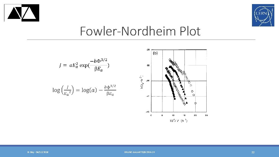
Fowler-Nordheim Plot BI Day - 04/12/2018 BRUNO. GALANTE@CERN. CH 22

SEM of CNT Array BI Day - 04/12/2018 BRUNO. GALANTE@CERN. CH 23
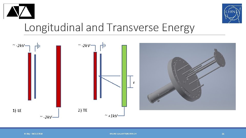
Longitudinal and Transverse Energy ~ -2 k. V r 2) TE 1) LE ~ -2 k. V BI Day - 04/12/2018 ~ +1 k. V BRUNO. GALANTE@CERN. CH 24

Grid vs Hole Grid BI Day - 04/12/2018 Hole BRUNO. GALANTE@CERN. CH 25
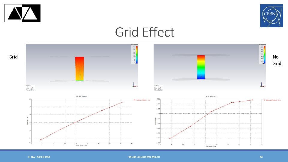
Grid Effect Grid No Grid BI Day - 04/12/2018 BRUNO. GALANTE@CERN. CH 26
- Slides: 26