Co Wo S FanOut Process Flow 20171229 3


")
 • In. FO ① Face Down(Die first)")
是一種整合生產技術,先將 晶片透過Chip on Wafer(Co. W)的封裝製程連接至矽晶圓,再把 Co. W晶片與基板連結,整合成Chip-on-Wafer-on-Substrate。 So. C")


 (pitch: 45 um) FPGA")


 Capacitors: 藉由在Si Interposer中用HD-MIM電容可以有供應的穩定電壓與減少電源處")
 HBM 2 (size: 8 x 12")


 • In. FO(Integrated Fan-Out) ① Face Down(Die")
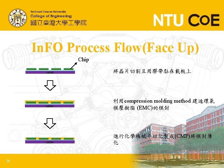
 Chip carrier 將晶片切割且用膠帶黏在載板上 carrier 利用compression molding method 建造環氧 模壓樹脂")
 加上RDL與錫球,封裝完成! 24")
 • In. FO(Integrated Fan-Out) ① Face Down(Die")
 carrier 加上RDL與錫球 去除載板 完成! 27")
 • In. FO(Integrated Fan-Out) ① Face Down(Die")
 Apply release layer on carrier 30 carrier RDL on")
 Carrier remove Solder ball attach 31")
 250 um BGA (H: 190)")
")

 • In. FO(Integrated Fan-Out) ① Face Down(Die")


- Slides: 37
Co. Wo. S & Fan-Out Process Flow 胡承維 2017/12/29
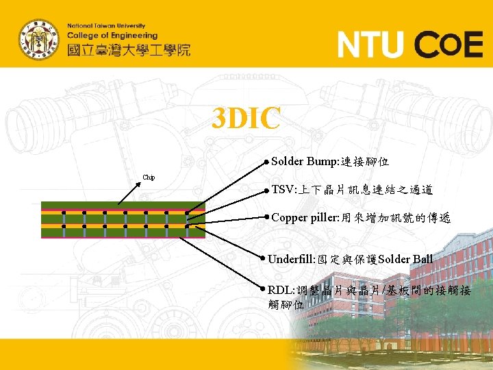
3 DIC為將許多晶片進行三維空間垂直整合 Chip TSV Underfill RDL Solder Ball PCB
2. 5 DIC 在晶片與基板之間加入Si interposer,藉由Si interposer整合晶 片並當作晶片與基板的連接橋梁。 ubump Underfill TSV Solder Ball PCB Substrate
Packaging Technology 目前主流晶片封裝方式: • Co. Wo. S • In. FO ① Face Down(Die first) ② Face Up(Die first) ③ Face Down(Die last) • In. FO_Po. P
Packaging Technology 目前主流晶片封裝方式: • Co. Wo. S(Chip-on-Wafer-on-Substrate) • In. FO ① Face Down(Die first) ② Face Up(Die first) ③ Face Down(Die last) • In. FO_Po. P
何謂Co. Wo. S? Co. Wo. S(Chip-on-Wafer-on-Substrate)是一種整合生產技術,先將 晶片透過Chip on Wafer(Co. W)的封裝製程連接至矽晶圓,再把 Co. W晶片與基板連結,整合成Chip-on-Wafer-on-Substrate。 So. C Wafer Co. W(Chip-on-Wafer) HBM PCB Substrate Co. Wo. S(Chip-on-Wafer-on-substrate)
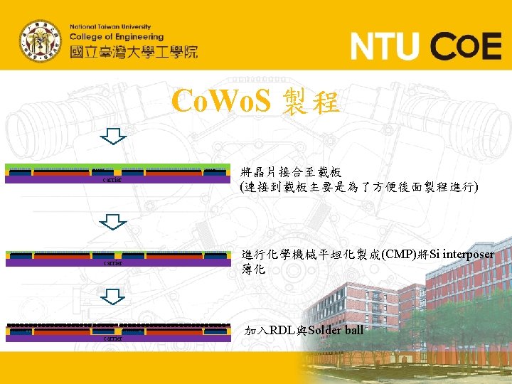
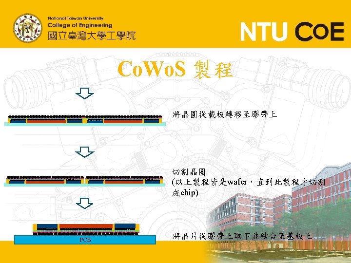
Co. Wo. S Process Flow So. C HBM 2 Top die Cu piller Solder ball Si interposer ubump: 一對Cu piller中間焊Solder Bottom die 先將Si interposer與晶片藉由ubump堆疊至 一起 填入Underfill保護晶片與連結的結構
Dimension of Co. Wo. S u. Bump (die: 20 um) (pitch: 45 um) FPGA (size: 7 x 23 mm 2) TSV (die: 12 um) (pitch: 180 um) C 4 bump (die: 80 um) (pitch: 180 um) PCB Substrate (size: 42. 5 x 42. 5 mm) Homogeneous Integration BGA (pitch: 100 mm)
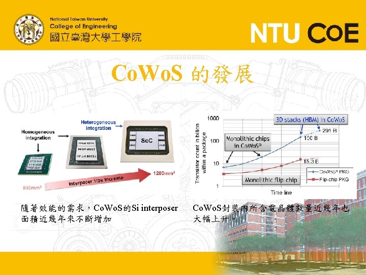
First-Generation of Co. Wo. S In 2012, TSMC successfully used Co. Wo. S® to integrate four 28 nm logic chips。 Homogeneous and heterogeneous interposer up to 800 mm 2 (Full reticle size) Homogeneous Integration (ex: Split Logic) Heterogeneous Integration (Logic + DRAM)
Second-Generation of Co. Wo. S 第二代Co. Wo. S為將Si interposer擴增到 1200 mm 2並結合fine pitch Cu bump, HBM 2 integration, and HD-MIM capacitors 使其有更好的效能。 Interposer PCB size: 1200 m 2
Second-Generation of Co. Wo. S Mask Stitching Technology: 由於Si interposer增加到 1200 mm 2,利用此技術將兩個光罩縫合製造出更 大的光罩以應用在Second-Generation Co. Wo. S上。 由左圖可知,在縫合後的光罩所製 造出來的RDL與一般無縫合的光罩 所製造出來的RDL其片電阻是幾乎 相同的。 Rs of normal and stitched 0. 4/0. 4 μm width/space RDL in ultralarge Si interposer.
Second-Generation of Co. Wo. S Fine Pitch Cu Bump: 藉由良好的間格和Cu bump與無鉛的銲錫連接,可以 減少傳統C 4 solder bump的bump bridge 問題。 C 4 Cu bumps at interposer corners remain undistorted after flip-chip bond process on a substrate. Cu bumps traditional solder bumps X-Ray images of Co. Wo. S package
Second-Generation of Co. Wo. S Integration of HD-MIM(High Density-Metal Insulator Metal) Capacitors: 藉由在Si Interposer中用HD-MIM電容可以有供應的穩定電壓與減少電源處 傳來的雜訊。 Integration of HBM 2: HBM 2提供更大的密度與頻寬。
Nvidia GP 100 Interposer (Area: 1200 mm 2) HBM 2 (size: 8 x 12 x 0. 72 mm) u. Bump(for HBM 2) (pitch: 96/55 um) Substrate (size: 55 x 1. 2 mm) 19 PCB BGA (pitch: 100 um)
About Co. Wo. S Application of Co. Wo. S : • AI • Server • Networking Characteristic of Co. Wo. S : • Ultra-high performance, So. C partition • Very high memory bandwidth • Wide envelope
Strengths of Co. Wo. S • • • 21 Fine RDL pitch & High TSV density Si interposer Fine pitch Micro-bump Assembly Fine gap Flip Chip underfill Co. W warpage control Large die reliability
Packaging Technology 目前主流晶片封裝方式: • Co. Wo. S(Chip-on-Wafer-on-Substrate) • In. FO(Integrated Fan-Out) ① Face Down(Die first) ② Face Up(Die first) ③ Face Down(Die last) • In. FO_Po. P
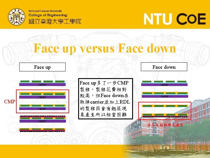
In. FO Process Flow(Face Down) Chip carrier 將晶片切割且用膠帶黏在載板上 carrier 利用compression molding method 建造環氧 模壓樹脂 (EMC)的模封 從膠帶上取下 23
In. FO Process Flow(Face Down) 加上RDL與錫球,封裝完成! 24
Packaging Technology 目前主流晶片封裝方式: • Co. Wo. S(Chip-on-Wafer-on-Substrate) • In. FO(Integrated Fan-Out) ① Face Down(Die first) ② Face Up(Die first) ③ Face Down(Die last) • In. FO_Po. P
In. FO Process Flow(Face Up) carrier 加上RDL與錫球 去除載板 完成! 27
Packaging Technology 目前主流晶片封裝方式: • Co. Wo. S(Chip-on-Wafer-on-Substrate) • In. FO(Integrated Fan-Out) ① Face Down(Die first) ② Face Up(Die first) ③ Face Down(Die last) • In. FO_Po. P
In. FO Process Flow(Die Last) Apply release layer on carrier 30 carrier RDL on the carrier Face-down attach carrier Molding
In. FO Process Flow(Die Last) Carrier remove Solder ball attach 31
Dimension of In. FO RDL (w/s: 5 um/5 um) 250 um BGA (H: 190) 32
About In. FO Application of In. FO : • Smart mobile(Apple A 10 Fusion) • Io. T • HPC Characteristics of In. FO : • Multi-chip Integration • Small form-factor • Cost competitive 33
Strengths of In. FO Compared with Flip-Chip, In. FO provides : • Low Power consumption • High Performance • Smaller thickness • Competitive cost 34
Packaging Technology 目前主流晶片封裝方式: • Co. Wo. S(Chip-on-Wafer-on-Substrate) • In. FO(Integrated Fan-Out) ① Face Down(Die first) ② Face Up(Die first) ③ Face Down(Die last) • In. FO_Po. P(Integrated Fan-Out_Package-on-Package)
In. FO_Po. P Process Flow Chip Pick&Place the chip on the carrier Molding Compound Cu-RDL and BGA 36
In. FO_Po. P Process Flow De-bound TIV : which is the In. FO-Po. P version of a through-silicon via (TSV), used with 3 D silicon interposer technology. Packaging & Stacking Memory So. C TIV 37 Dicing & shipping