Co Co Cockroft Walton Feedback Control Circuit On
Co. Co – Cockroft Walton Feedback Control Circuit On the behalf of Deepak G, Paul T, Vladimir G D. Gajanana ET 14 -02 -2012 1
Motivation for HV and its regulation… • 3” Photo Multiplier Tubes (PMT) operate with high voltage (HV) in the order of k. V. • The gain of the PMT varies linearly with HV. • The HV is generated using a Cockroft Walton (CW) multiplier circuit. • This HV should be regulated in order to have stable operation of the PMT. • No second source for the present driver D. Gajanana ET 14 -02 -2012 2
Present Solution using COTS component • AD 1111 • The input 7 μs DC pulses to the CW multiplier were supplied with a load dependent frequency between 1 and 5 k. Hz. • The circuit had stability problems at lower HV outputs. • The output load current rating was too high. • House keeping power high because its generic functions. • The COTS is also costly at low volume (~0. 5 M). D. Gajanana ET 14 -02 -2012 3
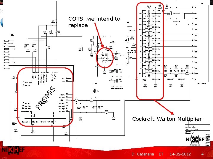
PR OM i. S COTS. . we intend to replace Cockroft-Walton Multiplier D. Gajanana ET 14 -02 -2012 4
Goals for Co. Co • Co. Co should regulate the frequency of the 6. 5 μs pulses. • For example, during start-up of the HV circuit, Co. Co should supply the pulses at a maximum of 50 k. Hz and when the desired HV is reached, the pulses are slowed down to a few Hz based on the feedback-> Low power operation . • The width of these pulses should also be controlled by sensing the current, to avoid saturation of the transformer. • The regulation should be stable, even at lower voltages. • Should have smaller footprint, cheaper and consume less power. D. Gajanana ET 14 -02 -2012 5
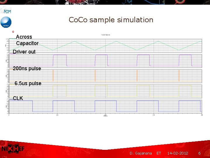
Co. Co sample simulation Across Capacitor Driver out 200 ns pulse 6. 5 us pulse CLK D. Gajanana ET 14 -02 -2012 6
Are we in line with the goal? • Co. Co is designed to control and regulate the feedback of the CW HV generator. • Co. Co is designed in 350 nm CMOS technology, consumes ~ 1. 7 m. W power. • Co. Co is stable even at lower CW voltages. D. Gajanana ET 14 -02 -2012 7
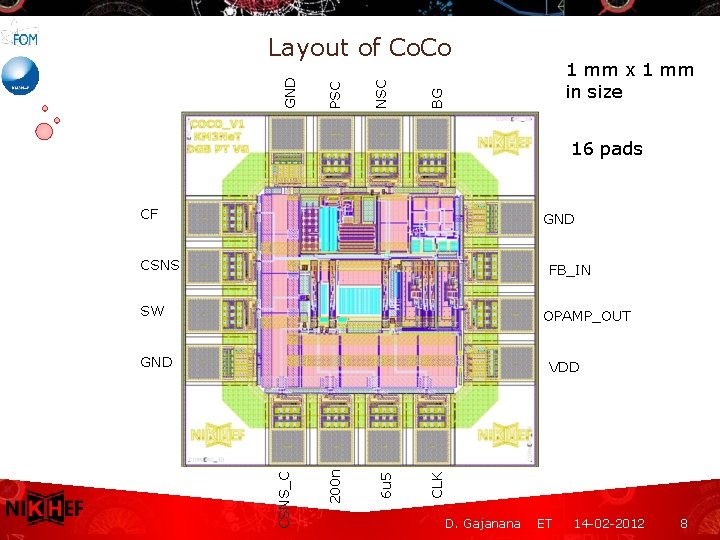
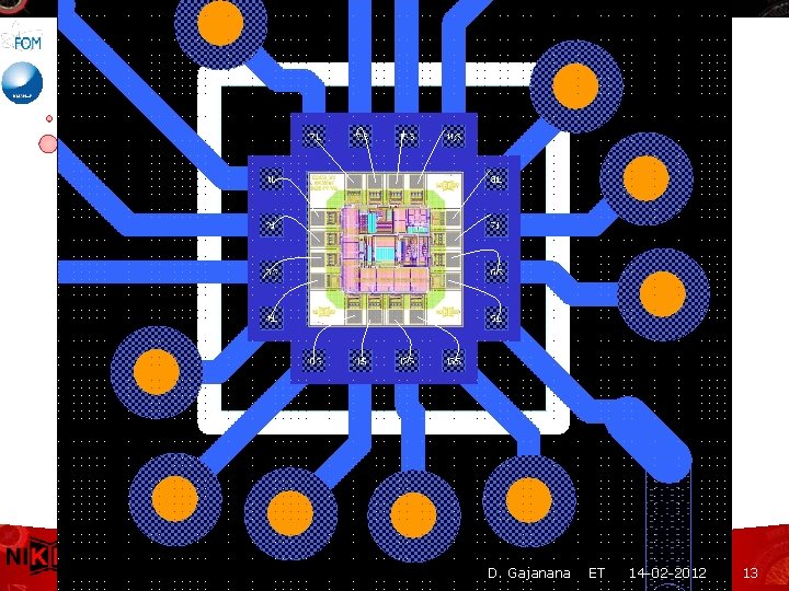
1 mm x 1 mm in size BG NSC PSC GND Layout of Co. Co 16 pads CF GND CSNS FB_IN SW OPAMP_OUT GND CLK 6 u 5 200 n CSNS_C VDD D. Gajanana ET 14 -02 -2012 8
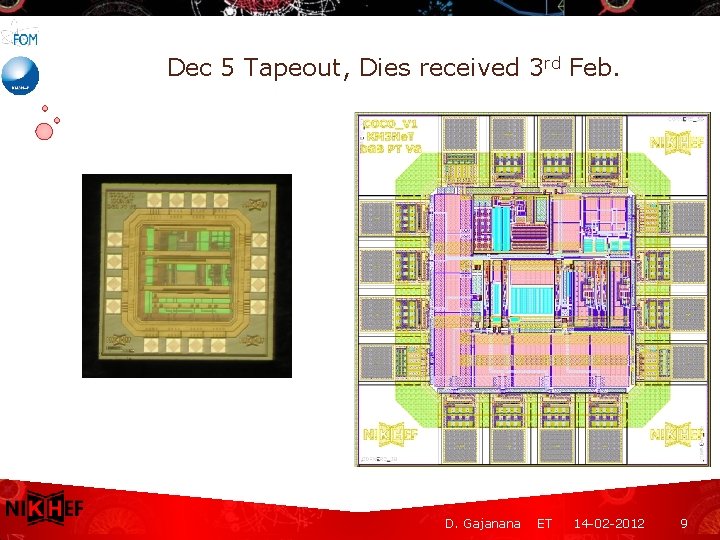
Dec 5 Tapeout, Dies received 3 rd Feb. D. Gajanana ET 14 -02 -2012 9
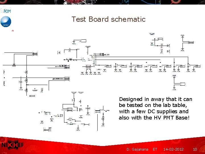
Test Board schematic Designed in away that it can be tested on the lab table, with a few DC supplies and also with the HV PMT Base! D. Gajanana ET 14 -02 -2012 10
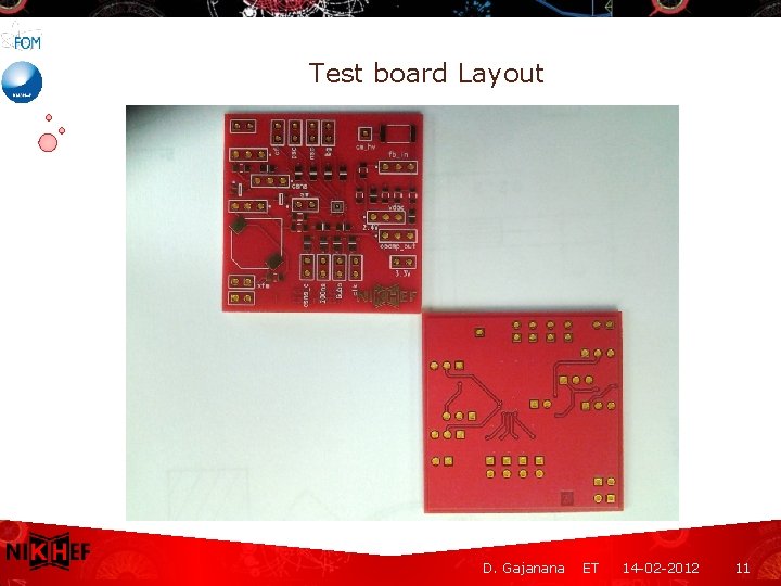
Test board Layout D. Gajanana ET 14 -02 -2012 11
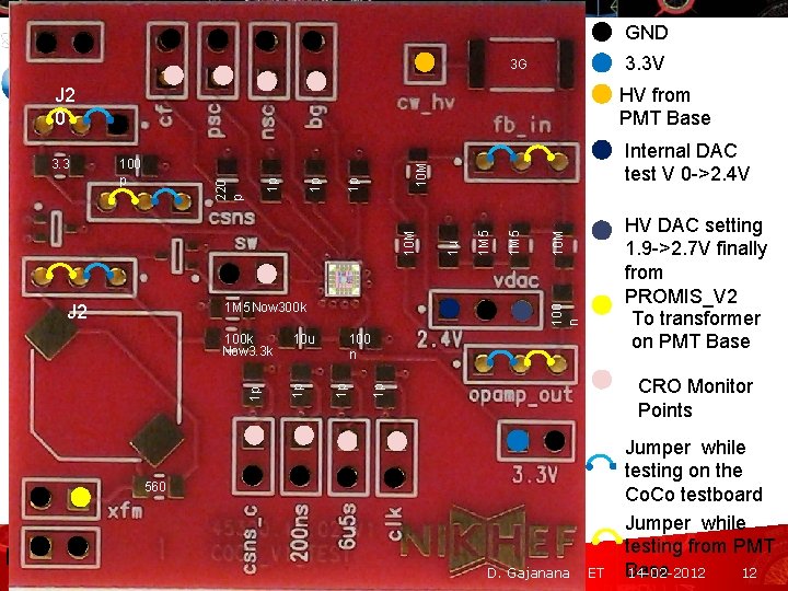
GND 3. 3 V 3 G 10 M 1 M 5 1 u 100 n CRO Monitor Points 1 p 1 p 10 u 1 p 1 p 100 k Now 3. 3 k HV DAC setting 1. 9 ->2. 7 V finally from PROMIS_V 2 To transformer on PMT Base 100 n 1 M 5 Now 300 k J 2 Internal DAC test V 0 ->2. 4 V 10 M 1 p 1 p 100 p 220 p 3. 3 HV from PMT Base 1 p J 2 0 560 D. Gajanana ET Jumper while testing on the Co. Co testboard Jumper while testing from PMT Base 14 -02 -2012 12
D. Gajanana ET 14 -02 -2012 13
Bonded Dies D. Gajanana ET 14 -02 -2012 14
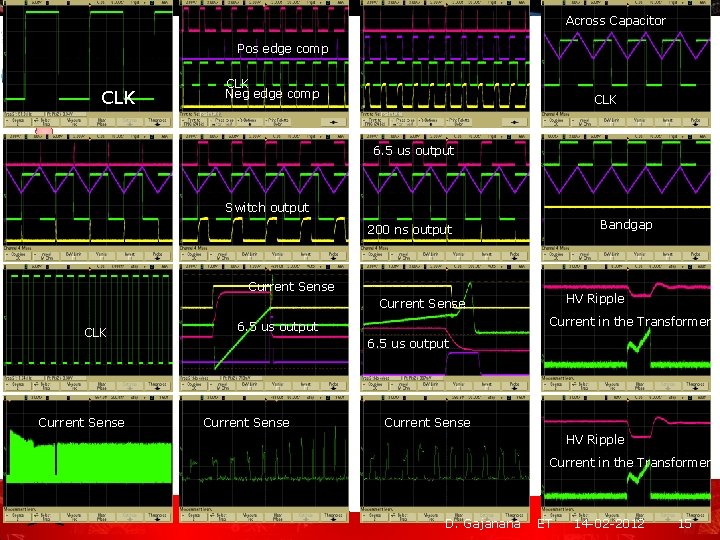
Across Capacitor Pos edge comp CLK Neg edge comp CLK 6. 5 us output Switch output Bandgap 200 ns output Current Sense HV Ripple Current Sense CLK Current Sense Current in the Transformer 6. 5 us output Current Sense HV Ripple Current in the Transformer D. Gajanana ET 14 -02 -2012 15
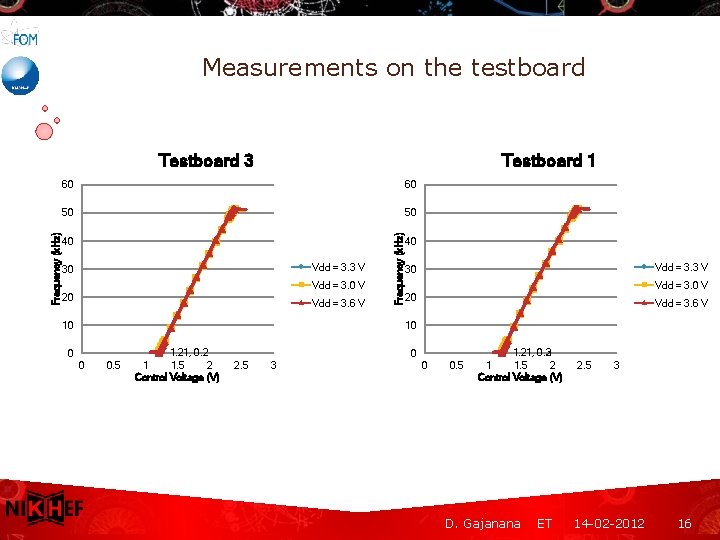
Measurements on the testboard Testboard 1 60 60 50 50 40 Vdd = 3. 3 V 30 Vdd = 3. 0 V 20 Vdd = 3. 6 V 10 Frequency (k. Hz) Testboard 3 40 Vdd = 3. 3 V 30 Vdd = 3. 0 V 20 Vdd = 3. 6 V 10 0 0 0. 5 1. 21, 0. 2 1 1. 5 2 Control Voltage (V) 0 2. 5 3 0 0. 5 0. 3 1. 21, 0. 2 1 1. 5 2 Control Voltage (V) D. Gajanana ET 2. 5 3 14 -02 -2012 16
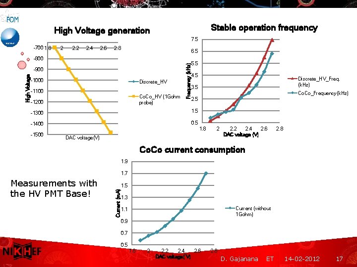
Stable operation frequency High Voltage generation 7. 5 -700 1. 8 2 2. 4 2. 6 2. 8 6. 5 High Voltage -900 -1000 Discrete_HV -1100 Co. Co_HV (1 Gohm probe) -1200 Frequency (k. Hz) -800 5. 5 4. 5 3. 5 Co. Co_Frequency(k. Hz) 2. 5 -1300 1. 5 -1400 0. 5 -1500 Discrete_HV_Freq. (k. Hz) 1. 8 2 DAC voltage(V) 2. 2 2. 4 2. 6 DAC voltage (V) 2. 8 Co. Co current consumption 1. 9 1. 7 1. 5 Current (m. A) Measurements with the HV PMT Base! 1. 3 Current (without 1 Gohm) 1. 1 0. 9 0. 7 0. 5 1. 8 2 2. 4 2. 6 DAC voltage( V) 2. 8 D. Gajanana ET 14 -02 -2012 17
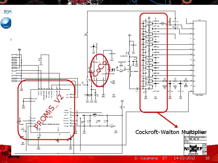
PR POR S MOi. SM _i V 2 Co Co COTS. . we intend to replace Cockroft-Walton Multiplier D. Gajanana ET 14 -02 -2012 18

Thank you for your attention D. Gajanana ET 14 -02 -2012 19
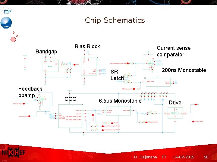
Chip Schematics Bandgap Bias Block Current sense comparator 200 ns Monostable SR Latch Feedback opamp CCO 6. 5 us Monostable D. Gajanana Driver ET 14 -02 -2012 20
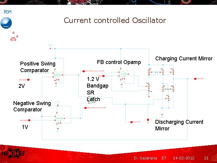
Current controlled Oscillator Positive Swing Comparator 2 V Negative Swing Comparator 1 V FB control Opamp Charging Current Mirror 1. 2 V Bandgap SR Latch Discharging Current Mirror D. Gajanana ET 14 -02 -2012 21
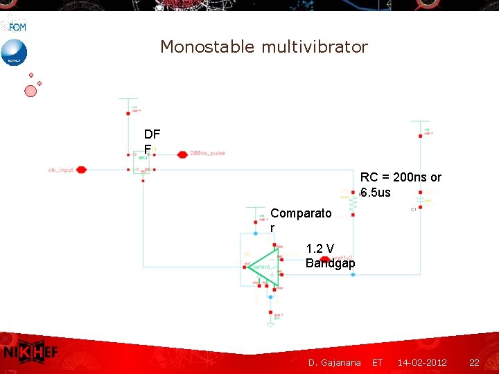
Monostable multivibrator DF F RC = 200 ns or 6. 5 us Comparato r 1. 2 V Bandgap D. Gajanana ET 14 -02 -2012 22
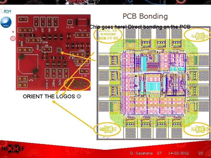
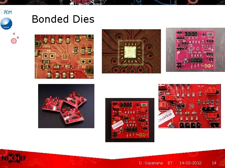
PCB Bonding Chip goes here! Direct bonding on the PCB ORIENT THE LOGOS D. Gajanana ET 14 -02 -2012 23
- Slides: 23