CMPUT 429 Winter 2002 Topic 5 Memory Technology






- Slides: 42

CMPUT 429 - Winter 2002 Topic 5: Memory Technology José Nelson Amaral CMPUT 429/CMPE 382 Computer Systems and Architecture 1

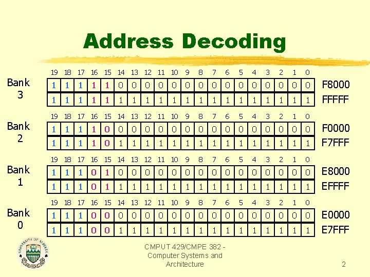
Address Decoding Bank 3 Bank 2 Bank 1 Bank 0 19 18 17 16 15 14 13 12 11 10 9 8 7 6 5 4 3 2 1 0 1 1 1 0 0 0 0 1 1 1 1 1 19 18 17 16 15 14 13 12 11 10 9 8 7 6 5 4 3 2 1 0 1 1 0 0 0 0 1 1 0 1 1 1 19 18 17 16 15 14 13 12 11 10 9 8 7 6 5 4 3 2 1 0 1 1 1 0 0 0 0 1 1 1 0 1 1 1 1 19 18 17 16 15 14 13 12 11 10 9 8 7 6 5 4 3 2 1 0 1 1 1 0 0 0 0 0 1 1 1 0 0 1 1 1 1 CMPUT 429/CMPE 382 Computer Systems and Architecture F 8000 FFFFF F 0000 F 7 FFF E 8000 EFFFF E 0000 E 7 FFF 2

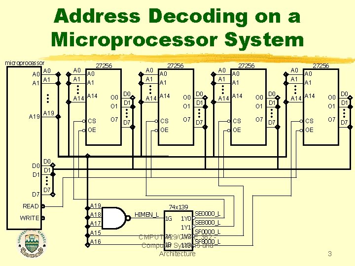
Address Decoding on a Microprocessor System microprocessor A 0 A 1 • • • A 19 27256 A 0 A 0 A 1 A 1 • • • D 0 O 0 A 14 A 14 D 1 O 1 • • • O 7 D 7 CS OE D 0 D 1 • • • D 7 READ WRITE A 19 A 18 A 17 A 15 A 16 74 x 139 SE 0000_L 1 Y 0 SE 8000_L 1 Y 1 SF 0000_L 1 Y 2 CMPUT 1 A 429/CMPE 382 SF 8000_L 1 B Systems 1 Y 3 Computer and HIMEN_L 1 G Architecture 3

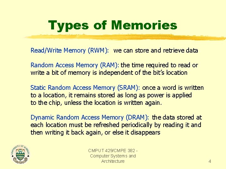
Types of Memories Read/Write Memory (RWM): we can store and retrieve data Random Access Memory (RAM): the time required to read or write a bit of memory is independent of the bit’s location Static Random Access Memory (SRAM): once a word is written to a location, it remains stored as long as power is applied to the chip, unless the location is written again. Dynamic Random Access Memory (DRAM): the data stored at each location must be refreshed periodically by reading it and then writing it back again, or else it disappears CMPUT 429/CMPE 382 Computer Systems and Architecture 4

Random Access Memories (RAMs) A Random-Access Memory (RAM) is so called to contrast with its predecessor, the Serial-Access Memory. In a serial access memory, memory positions become available for reading on a sequential fashion. Therefore to read an specific memory position, the reader must wait a variable time delay for the memory position to became available. In principle, in a RAM, all positions of the memory can be read on a random fashion with approximately the same delay for all positions. However, modern RAMs allow burst accesses that favor sequential accesses (complete them in less time). CMPUT 429/CMPE 382 Computer Systems and Architecture 5

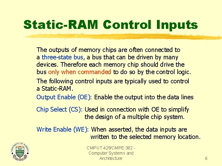
Static-RAM Control Inputs The outputs of memory chips are often connected to a three-state bus, a bus that can be driven by many devices. Therefore each memory chip should drive the bus only when commanded to do so by the control logic. The following control inputs are typically used to control a Static-RAM. Output Enable (OE): Enable the output into the data lines Chip Select (CS): Used in connection with OE to simplify the design of a multiple chip system. Write Enable (WE): When asserted, the data inputs are written to the selected memory location. CMPUT 429/CMPE 382 Computer Systems and Architecture 6

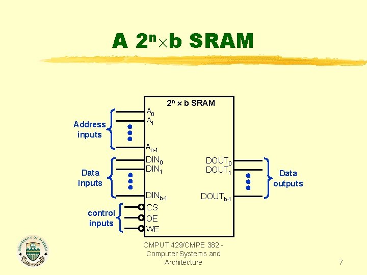
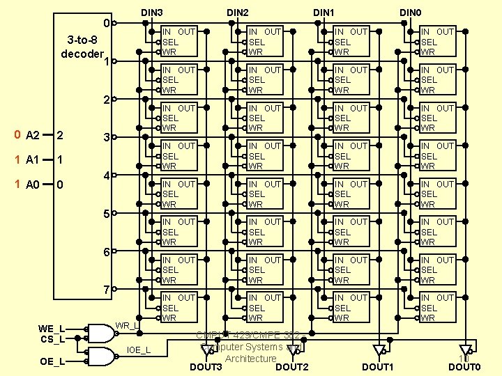
A 2 n b SRAM Address inputs A 0 A 1 2 n b SRAM An-1 Data inputs control inputs DIN 0 DIN 1 DOUT 0 DOUT 1 DINb-1 DOUTb-1 Data outputs CS OE WE CMPUT 429/CMPE 382 Computer Systems and Architecture 7

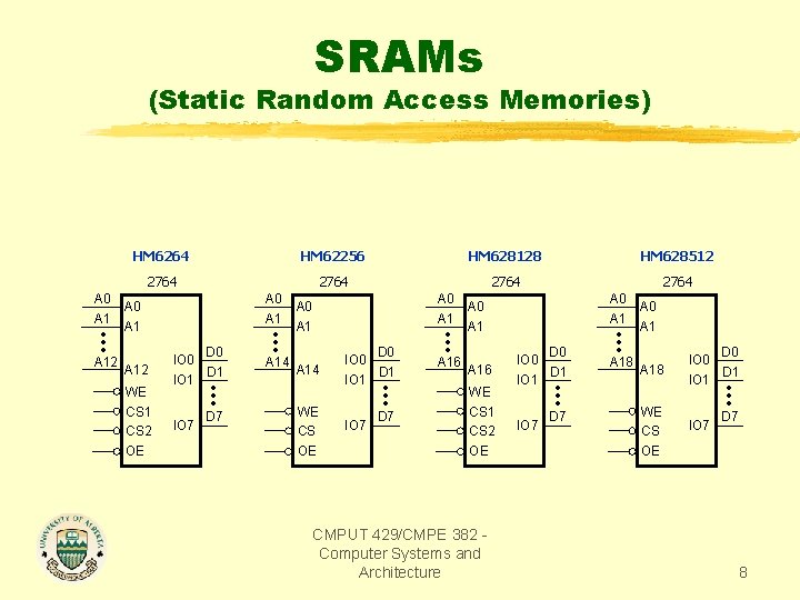
SRAMs (Static Random Access Memories) HM 6264 HM 62256 HM 628128 HM 628512 2764 A 0 A 1 • • • A 12 WE CS 1 CS 2 OE D 0 IO 0 D 1 IO 1 • • • D 7 IO 7 A 0 A 1 • • • A 14 WE CS OE D 0 IO 0 D 1 IO 1 • • • D 7 IO 7 A 0 A 1 • • • A 16 WE CS 1 CS 2 OE CMPUT 429/CMPE 382 Computer Systems and Architecture D 0 IO 0 D 1 IO 1 • • • D 7 IO 7 A 0 A 1 • • • A 18 WE CS OE D 0 IO 0 D 1 IO 1 • • • D 7 IO 7 8

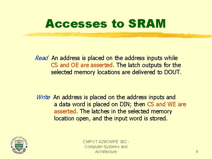
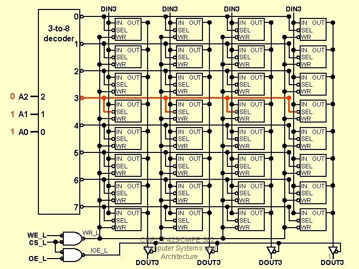
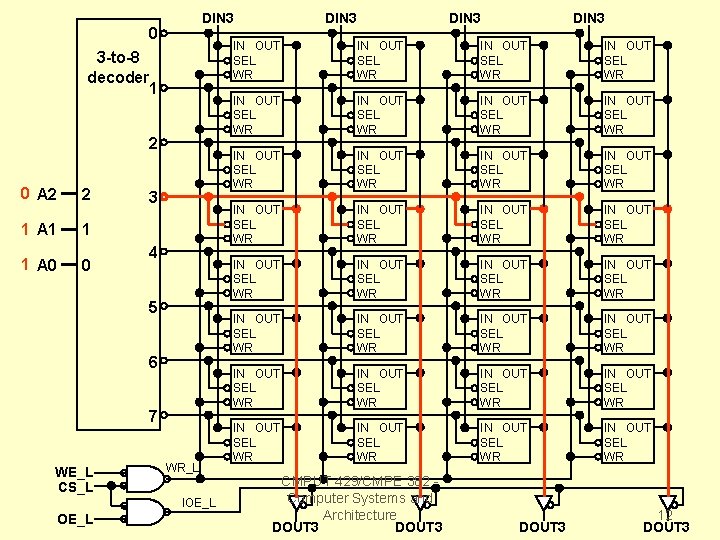
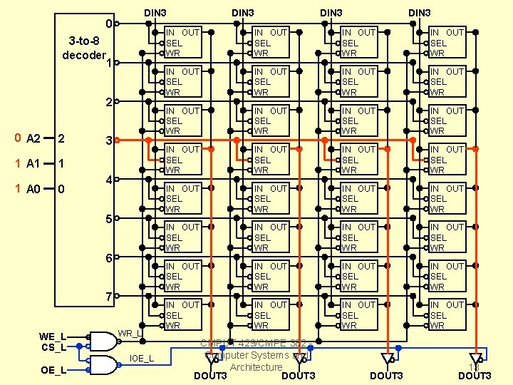
Accesses to SRAM Read An address is placed on the address inputs while CS and OE are asserted. The latch outputs for the selected memory locations are delivered to DOUT. Write An address is placed on the address inputs and a data word is placed on DIN; then CS and WE are asserted. The latches in the selected memory location open, and the input word is stored. CMPUT 429/CMPE 382 Computer Systems and Architecture 9

DIN 3 0 3 -to-8 decoder 1 2 0 A 2 2 1 A 1 1 1 A 0 0 3 4 5 6 7 WE_L CS_L WR_L IOE_L DIN 2 DIN 1 DIN 0 IN OUT SEL WR IN OUT SEL WR IN OUT SEL WR IN OUT SEL WR IN OUT SEL WR IN OUT SEL WR IN OUT SEL WR IN OUT SEL WR CMPUT 429/CMPE 382 Computer Systems and Architecture DOUT 3 DOUT 2 DOUT 1 10 DOUT 0

DIN 3 0 3 -to-8 decoder 1 2 0 A 2 2 1 A 1 1 1 A 0 0 3 4 5 6 7 WE_L CS_L WR_L IOE_L DIN 3 IN OUT SEL WR IN OUT SEL WR IN OUT SEL WR IN OUT SEL WR IN OUT SEL WR IN OUT SEL WR IN OUT SEL WR IN OUT SEL WR CMPUT 429/CMPE 382 Computer Systems and Architecture DOUT 3 11 DOUT 3

DIN 3 0 3 -to-8 decoder 1 2 0 A 2 2 1 A 1 1 1 A 0 0 3 4 5 6 7 WE_L CS_L WR_L IOE_L DIN 3 IN OUT SEL WR IN OUT SEL WR IN OUT SEL WR IN OUT SEL WR IN OUT SEL WR IN OUT SEL WR IN OUT SEL WR IN OUT SEL WR CMPUT 429/CMPE 382 Computer Systems and Architecture DOUT 3 12 DOUT 3

DIN 3 0 3 -to-8 decoder 1 2 0 A 2 2 1 A 1 1 1 A 0 0 3 4 5 6 7 WE_L CS_L WR_L IOE_L DIN 3 IN OUT SEL WR IN OUT SEL WR IN OUT SEL WR IN OUT SEL WR IN OUT SEL WR IN OUT SEL WR IN OUT SEL WR IN OUT SEL WR CMPUT 429/CMPE 382 Computer Systems and Architecture DOUT 3 13 DOUT 3

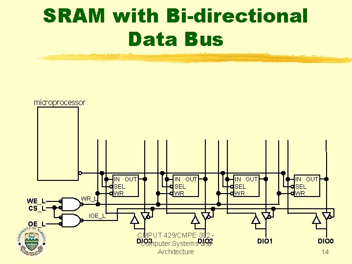
SRAM with Bi-directional Data Bus microprocessor WE_L CS_L WR_L IN OUT SEL WR IOE_L CMPUT 429/CMPE 382 DIO 3 Computer Systems. DIO 2 and Architecture DIO 1 DIO 0 14

Internal Address Decoding To avoid high complexity in the decoding logic, all memories (EPROMs, SRAMs, and DRAMs) use two-dimensional decoding which reduces the decoder size to approximately the square root of the number of addresses. The memory cells are organized in a two-dimensional array. Some address lines are used to select a row and the others are used to select a column. The cell selected by the whole address is at the intersection of the row and the column. CMPUT 429/CMPE 382 Computer Systems and Architecture 15

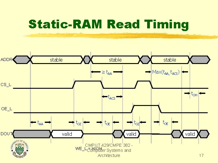
Static-RAM Read Timing t. AA (access time for address): how long it takes to get stable output after a change in address. t. ACS (access time for chip select): how long it takes to get stable output after CS is asserted. t. OE (output enable time): how long it takes for the three-state output buffers to leave the high-impedance state when OE and CS are both asserted. t. OZ (output-disable time): how long it takes for the three-state output buffers to enter high-impedance state after OE or CS are negated. t. OH (output-hold time): how long the output data remains CMPUT 429/CMPE 382 valid after a change to the address inputs. Computer Systems and Architecture 16

Static-RAM Read Timing stable ADDR stable t. AA Max(t. AA, t. ACS) CS_L t. OH t. ACS OE_L t. AA DOUT t. OZ valid t. OZ t. OE valid CMPUT 429/CMPE 382 WE_LComputer = HIGH Systems and Architecture t. OE valid 17

Static-RAM Write Timing t. AS (address setup time before write): all address inputs must be stable at this time before both CS and WE are asserted. t. AH(address hold time after write): all address inputs must be held stable until this time after CS or WE is negated. t. CSW (chip-select setup before end of write): CS must be asserted at least this long before the end of the write cycle. t. WP (write pulse width): WE must be asserted at least this long to reliably latch data into the selected cell. t. DS (data setup time before end of write): All of the data inputs must be stable at this time before the write cycle ends. t. DH (data hold time CMPUT after the end of write): All data inputs must 429/CMPE 382 be held stable until this Systems time after Computer and the write cycle ends. Architecture 18

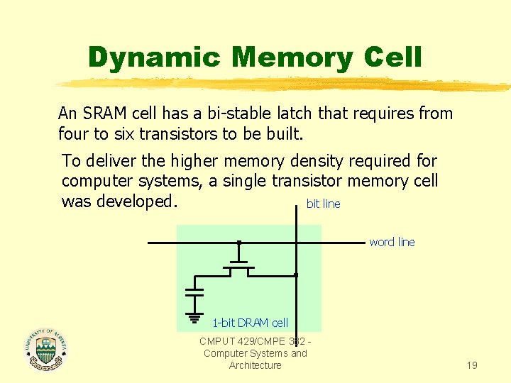
Dynamic Memory Cell An SRAM cell has a bi-stable latch that requires from four to six transistors to be built. To deliver the higher memory density required for computer systems, a single transistor memory cell was developed. bit line word line 1 -bit DRAM cell CMPUT 429/CMPE 382 Computer Systems and Architecture 19

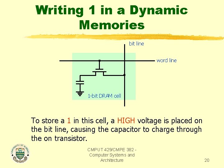
Writing 1 in a Dynamic Memories bit line word line 1 -bit DRAM cell To store a 1 in this cell, a HIGH voltage is placed on the bit line, causing the capacitor to charge through the on transistor. CMPUT 429/CMPE 382 Computer Systems and Architecture 20

Writing 0 in a Dynamic Memories bit line word line 1 -bit DRAM cell To store a 0 in this cell, a LOW voltage is placed on the bit line, causing the capacitor to discharge through the on transistor. CMPUT 429/CMPE 382 Computer Systems and Architecture 21

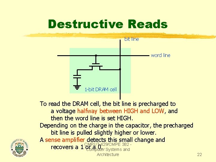
Destructive Reads bit line word line 1 -bit DRAM cell To read the DRAM cell, the bit line is precharged to a voltage halfway between HIGH and LOW, and then the word line is set HIGH. Depending on the charge in the capacitor, the precharged bit line is pulled slightly higher or lower. A sense amplifier detects this small change and CMPUT 429/CMPE 382 recovers a 1 or a 0. Systems and Computer Architecture 22

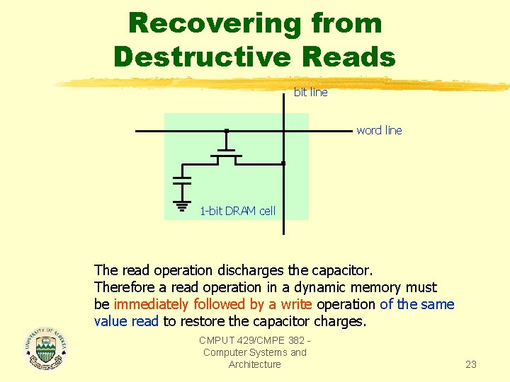
Recovering from Destructive Reads bit line word line 1 -bit DRAM cell The read operation discharges the capacitor. Therefore a read operation in a dynamic memory must be immediately followed by a write operation of the same value read to restore the capacitor charges. CMPUT 429/CMPE 382 Computer Systems and Architecture 23

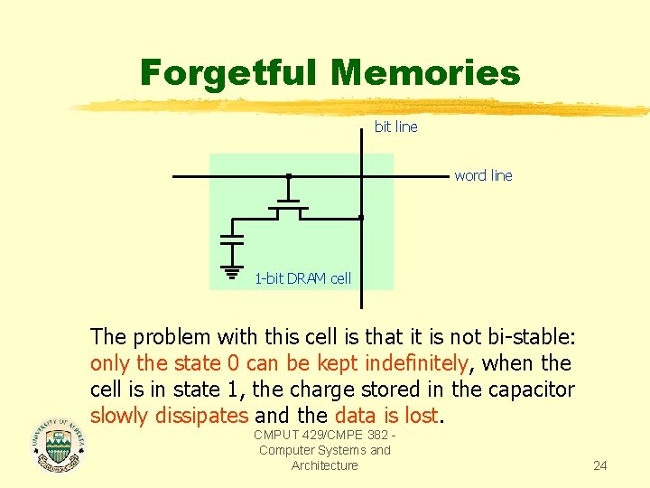
Forgetful Memories bit line word line 1 -bit DRAM cell The problem with this cell is that it is not bi-stable: only the state 0 can be kept indefinitely, when the cell is in state 1, the charge stored in the capacitor slowly dissipates and the data is lost. CMPUT 429/CMPE 382 Computer Systems and Architecture 24

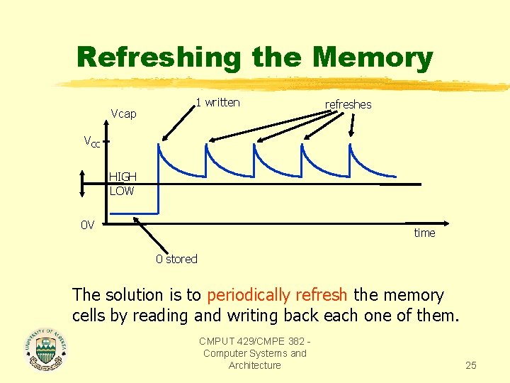
Refreshing the Memory Vcap 1 written refreshes VCC HIGH LOW 0 V time 0 stored The solution is to periodically refresh the memory cells by reading and writing back each one of them. CMPUT 429/CMPE 382 Computer Systems and Architecture 25

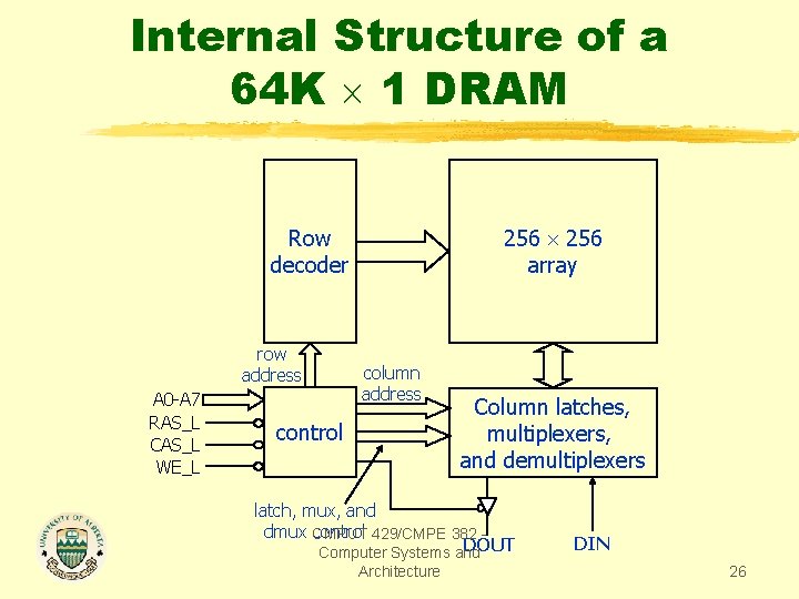
Internal Structure of a 64 K 1 DRAM 256 array Row decoder row address A 0 -A 7 RAS_L CAS_L WE_L column address control Column latches, multiplexers, and demultiplexers latch, mux, and dmux CMPUT control 429/CMPE 382 DOUT Computer Systems and Architecture DIN 26

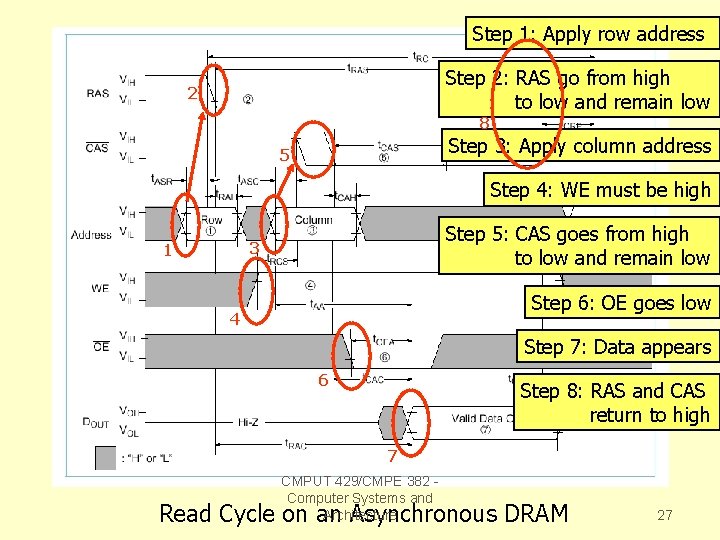
Step 1: Apply row address Step 2: RAS go from high to low and remain low 2 8 Step 3: Apply column address 5 Step 4: WE must be high Step 5: CAS goes from high to low and remain low 3 1 Step 6: OE goes low 4 Step 7: Data appears 6 Step 8: RAS and CAS return to high 7 CMPUT 429/CMPE 382 Computer Systems and Architecture Read Cycle on an Asynchronous DRAM 27

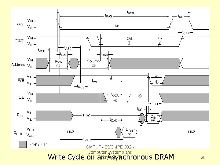
CMPUT 429/CMPE 382 Computer Systems and Architecture Write Cycle on an Asynchronous DRAM 28

Improved DRAMs Central Idea: Each read to a DRAM actually reads a complete row of bits or word line from the DRAM core into an array of sense amps. A traditional asynchronous DRAM interface then selects a small number of these bits to be delivered to the cache/microprocessor. All the other bits already extracted from the DRAM cells into the sense amps are wasted. CMPUT 429/CMPE 382 Computer Systems and Architecture 29

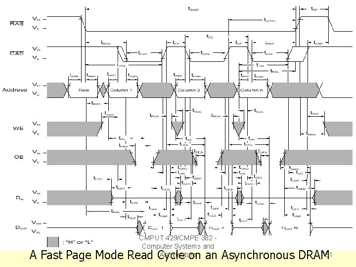
Fast Page Mode DRAMs In a DRAM with Fast Page Mode, a page is defined as all memory addresses that have the same row address. To read in fast page mode, all the steps from 1 to 7 of a standard read cycle are performed. Then OE and CAS are switched high, but RAS remains low. Then the steps 3 to 7 (providing a new column address, asserting CAS and OE) are performed for each new memory location to be read. CMPUT 429/CMPE 382 Computer Systems and Architecture 30

CMPUT 429/CMPE 382 Computer Systems and Architecture A Fast Page Mode Read Cycle on an Asynchronous DRAM 31

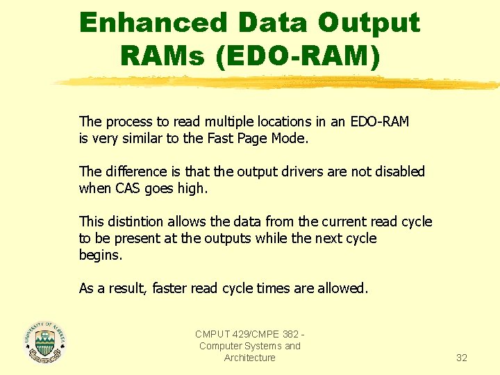
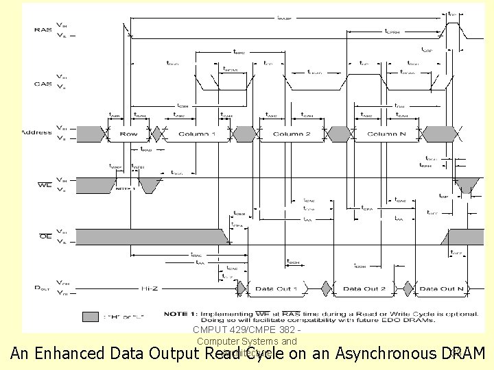
Enhanced Data Output RAMs (EDO-RAM) The process to read multiple locations in an EDO-RAM is very similar to the Fast Page Mode. The difference is that the output drivers are not disabled when CAS goes high. This distintion allows the data from the current read cycle to be present at the outputs while the next cycle begins. As a result, faster read cycle times are allowed. CMPUT 429/CMPE 382 Computer Systems and Architecture 32

CMPUT 429/CMPE 382 Computer Systems and Architecture 33 An Enhanced Data Output Read Cycle on an Asynchronous DRAM

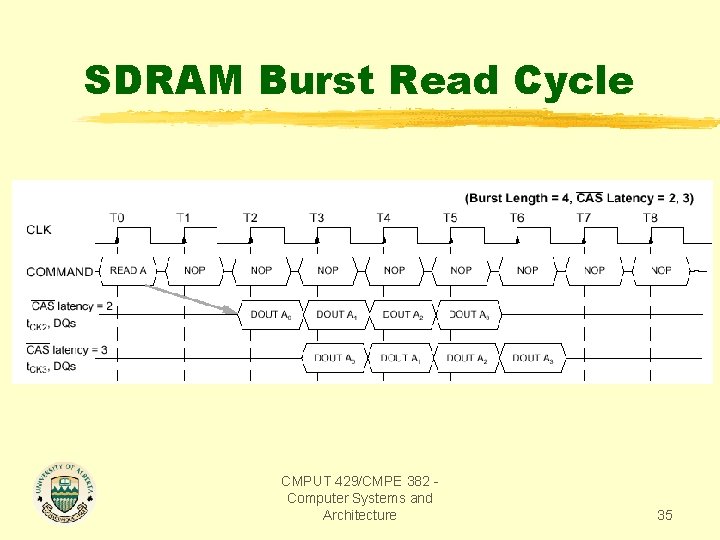
Synchronous DRAMs (SDRAM) A Synchronous DRAM (SDRAM) has a clock input. It operates in a similar fashion as the fast page mode and EDO DRAM. However the consecutive data is output synchronously on the falling/rising edge of the clock, instead of on command by CAS. How many data elements will be output (the length of the burst) is programmable up to the maximum size of the row. The clock in an SDRAM typically runs one order of magnitude faster than the access time for individual accesses. CMPUT 429/CMPE 382 Computer Systems and Architecture 34

SDRAM Burst Read Cycle CMPUT 429/CMPE 382 Computer Systems and Architecture 35

DDR SDRAM A Double Data Rate (DDR) SDRAM is an SDRAM that allows data transfers both on the rising and falling edge of the clock. Thus the effective data transfer rate of a DDR SDRAM is two times the data transfer rate of a standard SDRAM with the same clock frequency. CMPUT 429/CMPE 382 Computer Systems and Architecture 36

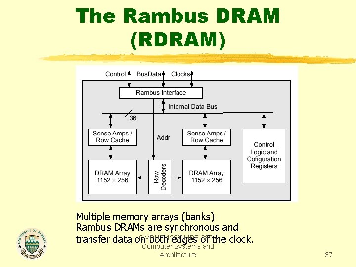
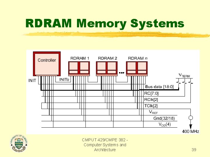
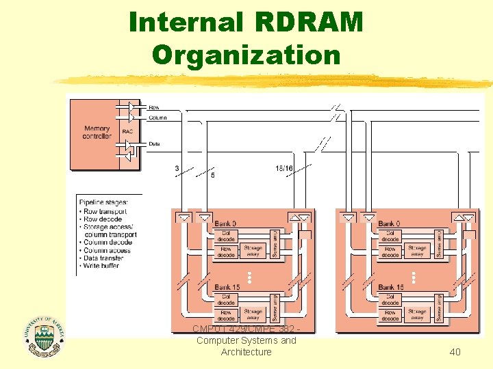
The Rambus DRAM (RDRAM) Multiple memory arrays (banks) Rambus DRAMs are synchronous and CMPUT 382 the transfer data on both 429/CMPE edges of clock. Computer Systems and Architecture 37

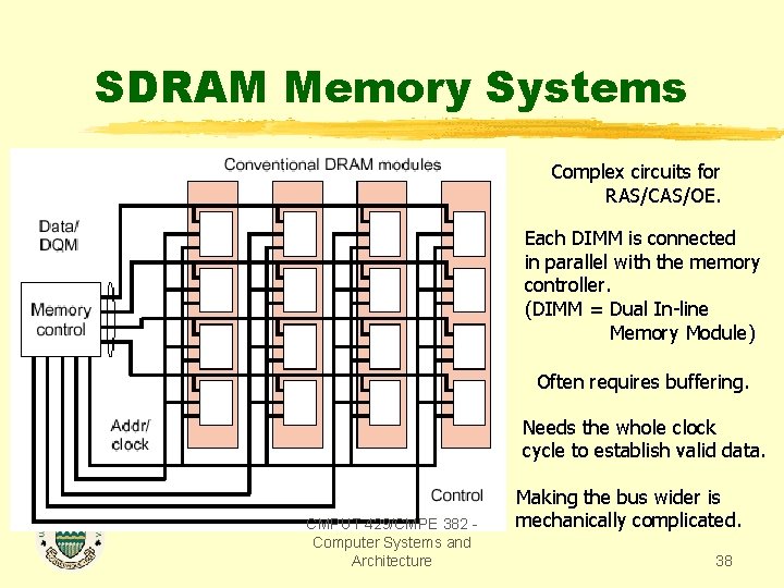
SDRAM Memory Systems Complex circuits for RAS/CAS/OE. Each DIMM is connected in parallel with the memory controller. (DIMM = Dual In-line Memory Module) Often requires buffering. Needs the whole clock cycle to establish valid data. CMPUT 429/CMPE 382 Computer Systems and Architecture Making the bus wider is mechanically complicated. 38

RDRAM Memory Systems CMPUT 429/CMPE 382 Computer Systems and Architecture 39

Internal RDRAM Organization CMPUT 429/CMPE 382 Computer Systems and Architecture 40

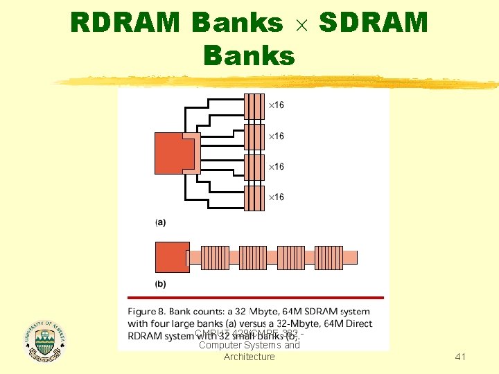
RDRAM Banks SDRAM Banks CMPUT 429/CMPE 382 Computer Systems and Architecture 41

Further Reading To learn more about the differences between SDRAM systems and Rambus DRAM systems for personal computers, visit these websites: http: //www. hardwarecentral. com/hardwarecentral/reviews/1787/1/ http: //www. pcguide. com/ref/ram/tech_SDRAM. htm Crisp, Richard, “Direct Rambus Technology: The New Main Memory Standard, ” IEEE Micro, 17(6): 18 -28, Nov/Dec, 1997. CMPUT 429/CMPE 382 Computer Systems and Architecture 42