CMOS VLSI Analog Design CMOS VLSI 1 Outline


- Slides: 34

CMOS VLSI Analog Design CMOS VLSI 1

Outline q Overview – Small signal model, biasing q Amplifiers – Common source, CMOS inverter – Current mirrors, Differential pairs – Operational amplifier q Data converters – DAC, ADC q RF – LNA, mixer Analog Design CMOS VLSI 2

CMOS for Analog q MOS device can be used for amplification as well as switching – Typical: operate devices in saturation, gate voltage sets current q Benefits – Cheap processes (compared to BJT) – Integrated packages q Challenges – Low gain – Coupling issues – Tolerances Analog Design CMOS VLSI 3

MOS Small Signal Model Analog Design CMOS VLSI 4

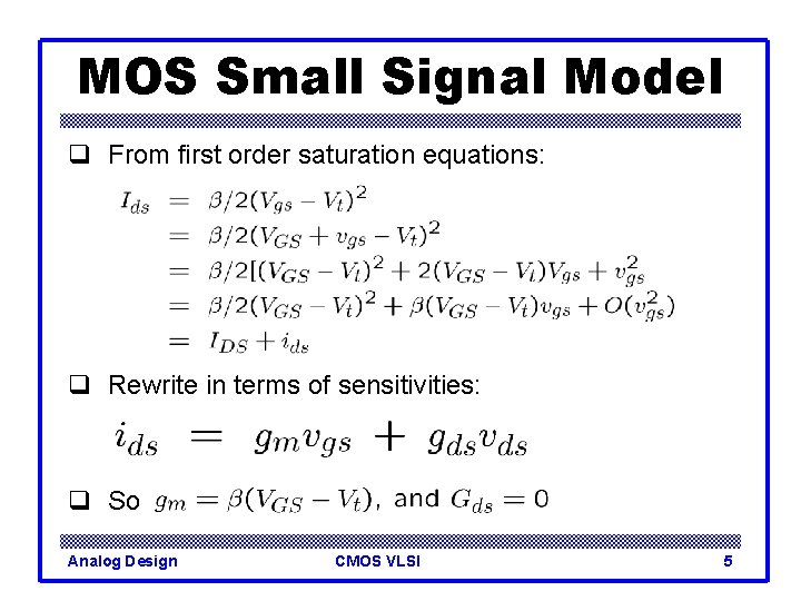
MOS Small Signal Model q From first order saturation equations: q Rewrite in terms of sensitivities: q So Analog Design CMOS VLSI 5

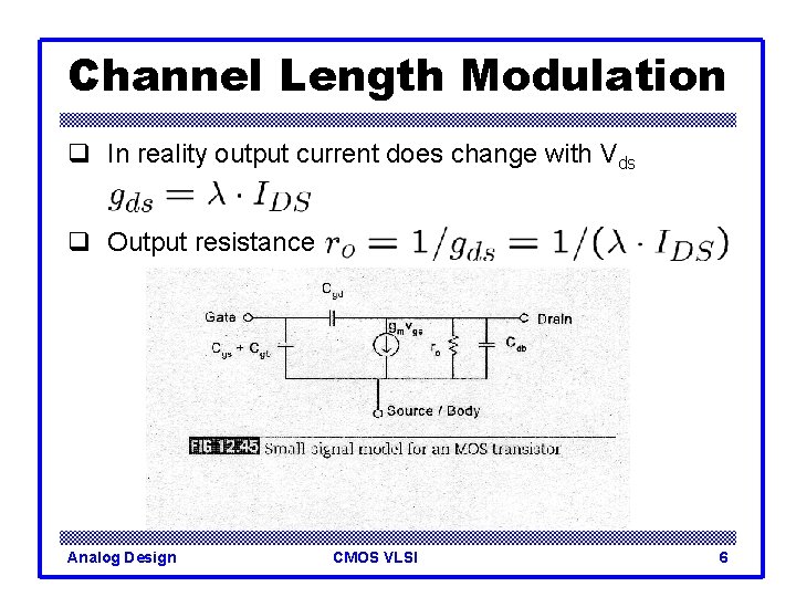
Channel Length Modulation q In reality output current does change with Vds q Output resistance Analog Design CMOS VLSI 6

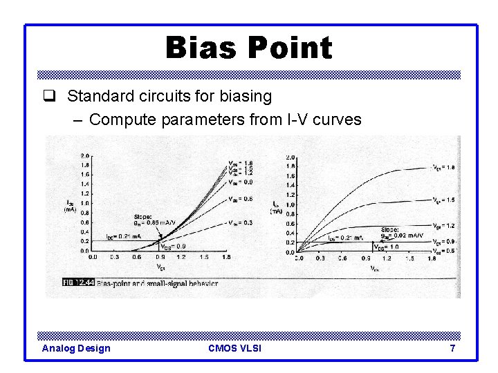
Bias Point q Standard circuits for biasing – Compute parameters from I-V curves Analog Design CMOS VLSI 7

Outline q Overview – Small signal model, biasing q Amplifiers – Common source, CMOS inverter – Current mirrors, Differential pairs – Operational amplifier q Data converters – DAC, ADC q RF – LNA, mixer Analog Design CMOS VLSI 8

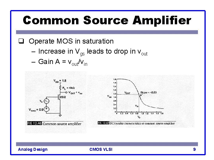
Common Source Amplifier q Operate MOS in saturation – Increase in Vgs leads to drop in vout – Gain A = vout/vin Analog Design CMOS VLSI 9

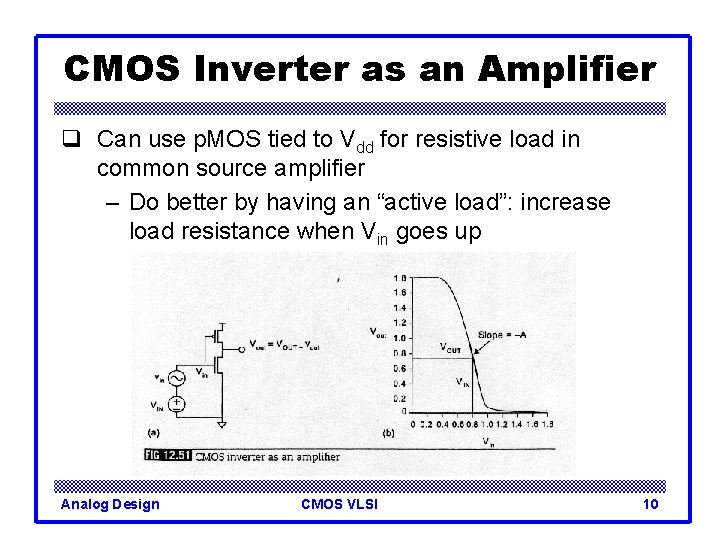
CMOS Inverter as an Amplifier q Can use p. MOS tied to Vdd for resistive load in common source amplifier – Do better by having an “active load”: increase load resistance when Vin goes up Analog Design CMOS VLSI 10

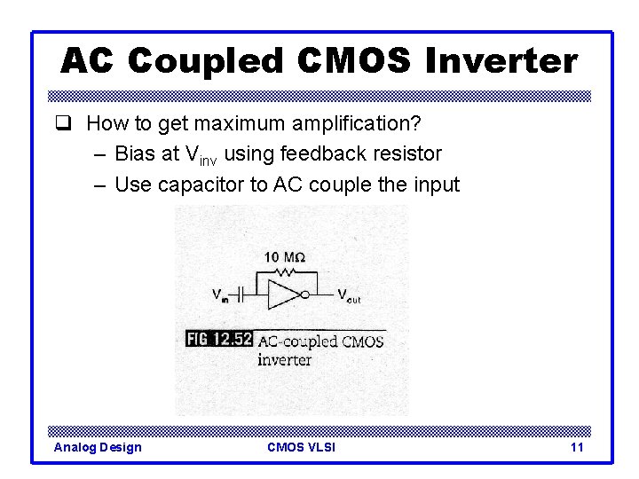
AC Coupled CMOS Inverter q How to get maximum amplification? – Bias at Vinv using feedback resistor – Use capacitor to AC couple the input Analog Design CMOS VLSI 11

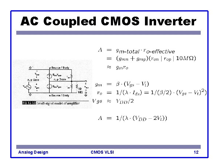
AC Coupled CMOS Inverter Analog Design CMOS VLSI 12

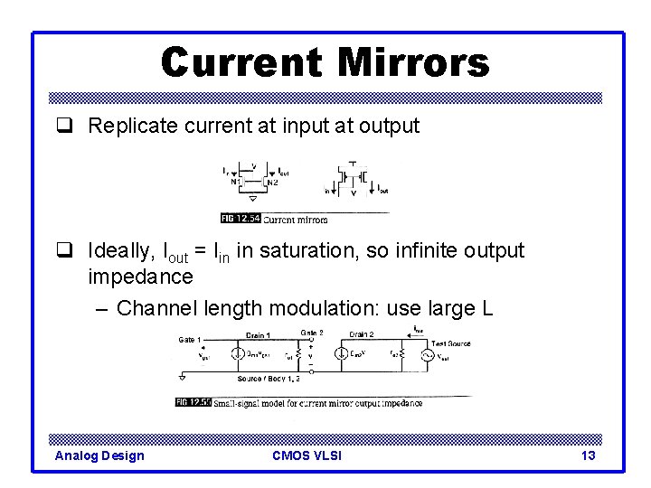
Current Mirrors q Replicate current at input at output q Ideally, Iout = Iin in saturation, so infinite output impedance – Channel length modulation: use large L Analog Design CMOS VLSI 13

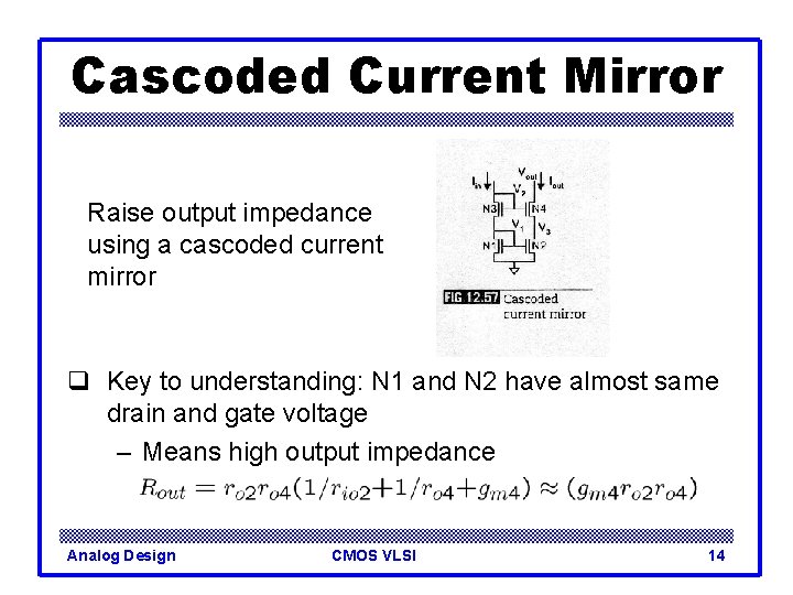
Cascoded Current Mirror Raise output impedance using a cascoded current mirror q Key to understanding: N 1 and N 2 have almost same drain and gate voltage – Means high output impedance Analog Design CMOS VLSI 14

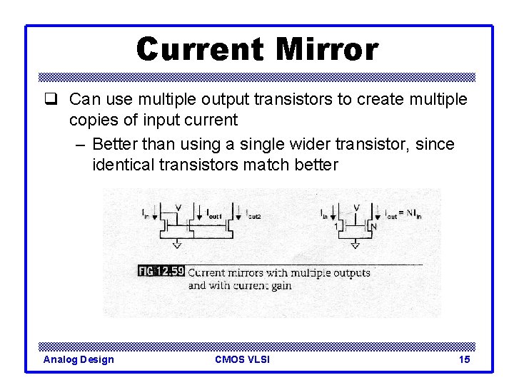
Current Mirror q Can use multiple output transistors to create multiple copies of input current – Better than using a single wider transistor, since identical transistors match better Analog Design CMOS VLSI 15

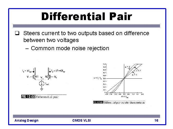
Differential Pair q Steers current to two outputs based on difference between two voltages – Common mode noise rejection Analog Design CMOS VLSI 16

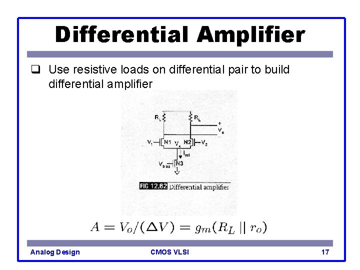
Differential Amplifier q Use resistive loads on differential pair to build differential amplifier Analog Design CMOS VLSI 17

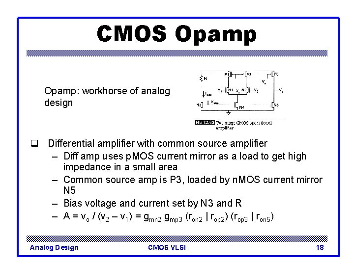
CMOS Opamp: workhorse of analog design q Differential amplifier with common source amplifier – Diff amp uses p. MOS current mirror as a load to get high impedance in a small area – Common source amp is P 3, loaded by n. MOS current mirror N 5 – Bias voltage and current set by N 3 and R – A = vo / (v 2 – v 1) = gmn 2 gmp 3 (ron 2 | rop 2) (rop 3 | ron 5) Analog Design CMOS VLSI 18

Outline q Overview – Small signal model, biasing q Amplifiers – Common source, CMOS inverter – Current mirrors, Differential pairs – Operational amplifier q Data converters – DAC, ADC q RF – LNA, mixer Analog Design CMOS VLSI 19

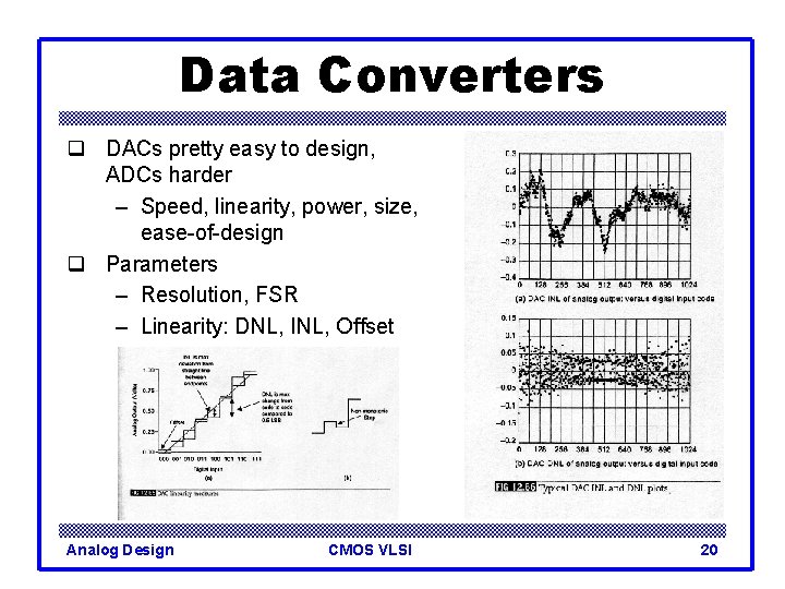
Data Converters q DACs pretty easy to design, ADCs harder – Speed, linearity, power, size, ease-of-design q Parameters – Resolution, FSR – Linearity: DNL, INL, Offset Analog Design CMOS VLSI 20

Noise and Distortion Measures q DAC: apply digital sine wave, measure desired signal energy to harmonics and noise q ADC: apply analog sine wave, do FFT on the stored samples – Measure total harmonic distortion (THD), and spurious free dynamic range (SFDR) Analog Design CMOS VLSI 21

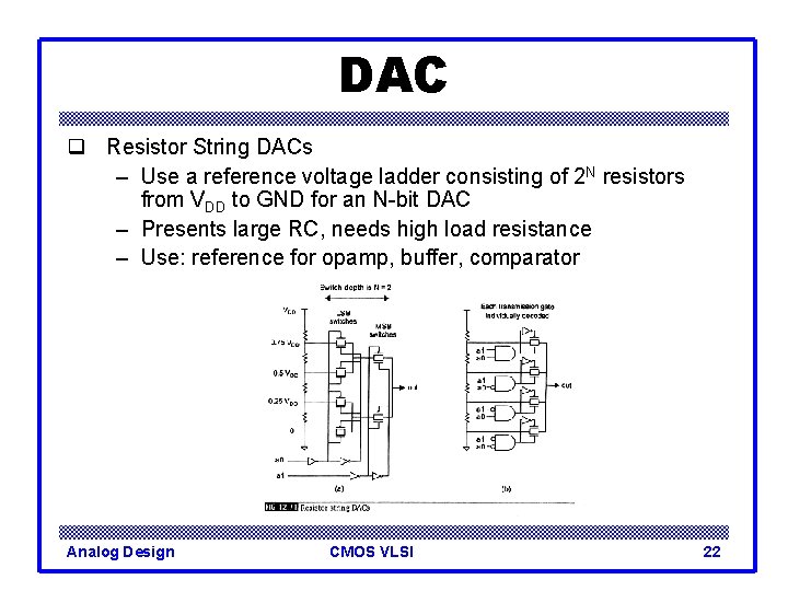
DAC q Resistor String DACs – Use a reference voltage ladder consisting of 2 N resistors from VDD to GND for an N-bit DAC – Presents large RC, needs high load resistance – Use: reference for opamp, buffer, comparator Analog Design CMOS VLSI 22

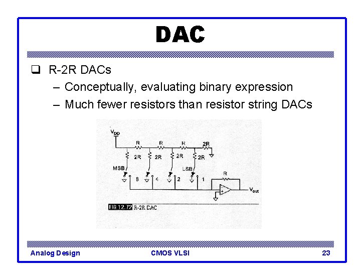
DAC q R-2 R DACs – Conceptually, evaluating binary expression – Much fewer resistors than resistor string DACs Analog Design CMOS VLSI 23

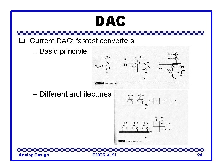
DAC q Current DAC: fastest converters – Basic principle – Different architectures Analog Design CMOS VLSI 24

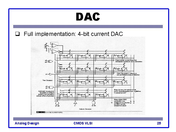
DAC q Full implementation: 4 -bit current DAC Analog Design CMOS VLSI 25

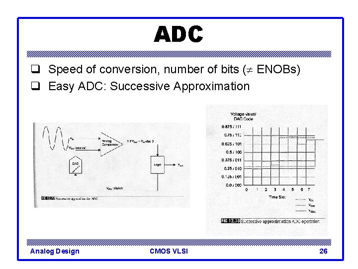
ADC q Speed of conversion, number of bits (¹ ENOBs) q Easy ADC: Successive Approximation Analog Design CMOS VLSI 26

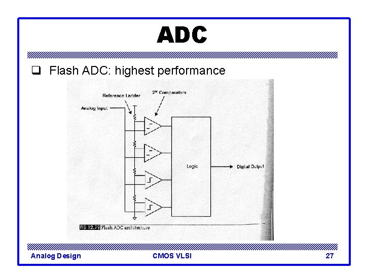
ADC q Flash ADC: highest performance Analog Design CMOS VLSI 27

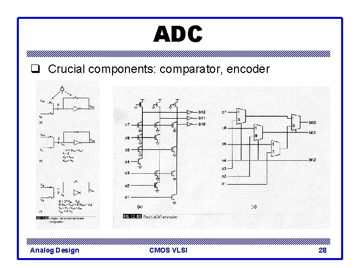
ADC q Crucial components: comparator, encoder Analog Design CMOS VLSI 28

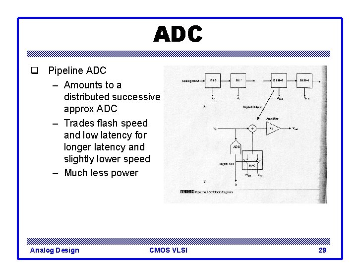
ADC q Pipeline ADC – Amounts to a distributed successive approx ADC – Trades flash speed and low latency for longer latency and slightly lower speed – Much less power Analog Design CMOS VLSI 29

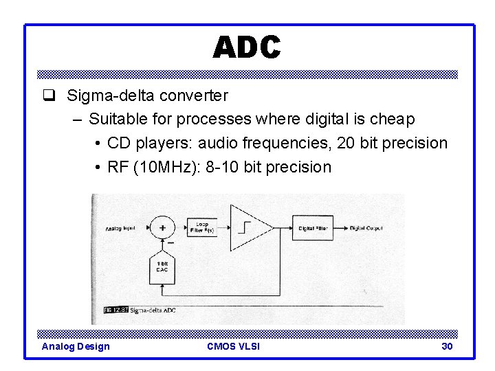
ADC q Sigma-delta converter – Suitable for processes where digital is cheap • CD players: audio frequencies, 20 bit precision • RF (10 MHz): 8 -10 bit precision Analog Design CMOS VLSI 30

Outline q Overview – Small signal model, biasing q Amplifiers – Common source, CMOS inverter – Current mirrors, Differential pairs – Operational amplifier q Data converters – DAC, ADC q RF – LNA, mixers Analog Design CMOS VLSI 31

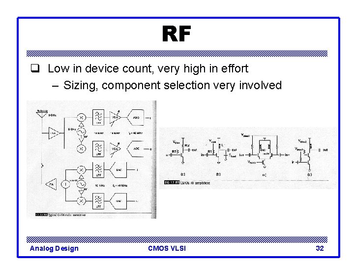
RF q Low in device count, very high in effort – Sizing, component selection very involved Analog Design CMOS VLSI 32

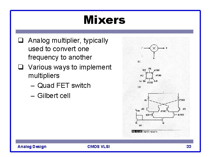
Mixers q Analog multiplier, typically used to convert one frequency to another q Various ways to implement multipliers – Quad FET switch – Gilbert cell Analog Design CMOS VLSI 33

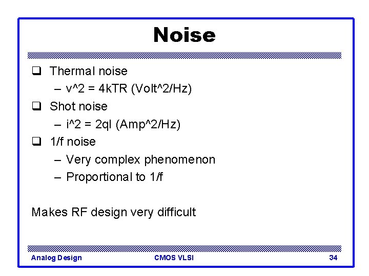
Noise q Thermal noise – v^2 = 4 k. TR (Volt^2/Hz) q Shot noise – i^2 = 2 q. I (Amp^2/Hz) q 1/f noise – Very complex phenomenon – Proportional to 1/f Makes RF design very difficult Analog Design CMOS VLSI 34