CMOS Technology Flow varies with process types company

 • p. MOS transistors in n-well • n. MOS")


- Slides: 18
CMOS Technology • Flow varies with process types & company – N-Well CMOS – Twin-Well CMOS – STI • Start with substrate selection – Type: n or p – Doping level, →resistivity – Orientation, 100, or 101, etc – Other parameters
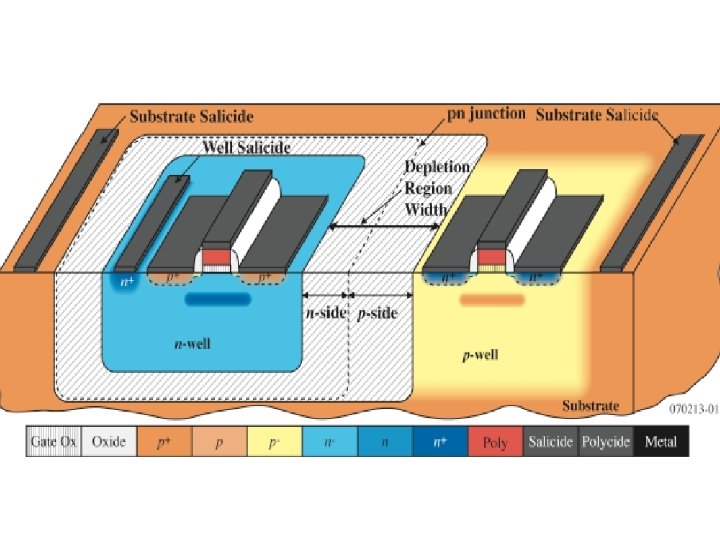
N-well CMOS (ON. 5 um) • p. MOS transistors in n-well • n. MOS transistors on substrate • n. MOS transistor’s body is always connected to lowest voltage of chip – n. MOS is a three terminal device • p. MOS body can be tied to voltages other than Vdd – p. MOS is a four terminal device • 0. 35 um and larger typically n-well
VDD M 2 Vin Vo M 1
Relative size of different layers
Deep Sub. Micron Challenges • Transistor sizes become very small • But FOX lateral size cannot be reduced • Depletion region between p-well and nwell not reduced • Large area FOX depletion
Shallow Trench Isolation Technology • Allowing transistors to be spaced closer
Devices available Transistors and wires Deep wells good for substrate noise isolation
Resistors • • • Diffused and/or implanted resistors. Well resistors. Polysilicon resistors. Metal resistors. Thin film resistors
capacitors Junction capacitors Gate capacitors Poly-poly capacitors Metal-metal capacitors In older processes, you put the bottom plate on FOX
Metal-metal capacitors Very linear cap More expensive to make
Inductors
Sub 100 nm CMOS Technology • • State of the art is 14 nm 45 nm is in wide use for high speed 65 nm also in wide use for So. Cs Grad students in our group have access to certain 28 nm, 45 nm, 65 nm, 130 nm, 180 nm, 0. 5 mm technologies – Have designed in such technologies – But analog transistors use L = 0. 6, 0. 9 mm
HW • Go to the MOSIS webpage • Find and download the NDA for IBM 0. 13 • Sign it, either give to TA in person, or scan and email to TA
Advantages • Digital Viewpoint: – – – Improved Ion/Ioff Reduced gate capacitance Higher drive current capability Reduced interconnect density Reduction of active power • Analog Viewpoint: – – More levels of metal Higher f. T Higher capacitance density Reduced junction capacitance per gm
Disadvantages for analog • Reduction in power supply resulting in reduced headroom and signal power • Gate leakage currents • Reduced small-signal intrinsic gains • Increased nonlinearity (IIP 3) • Noise and matching? ? • Reduced signal to noise ratio Anne-Johan Annema, et. Al. , “Analog Circuits in Ultra-Deep-Submicron CMOS, ” IEEE J. of Solid-State Circuits, Vol. 40, No. 1, Jan. 2005, pp. 132 -143.
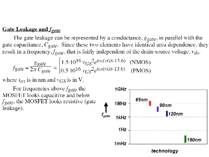
the Gate Leakage Problem