CMOS Technology and Logic Gates Only 15 432
- Slides: 37

CMOS Technology and Logic Gates Only 15, 432, 758 more mosfets to do. . . metal poly 6. 884 – Spring 2005 pdiff 2/07/2005 ndiff L 03 – CMOS Technology 1

Quality of Design Quality of a hardware design primarily judged by: – Price – Performance – Power and/or Energy Other important metrics can include: – Operating range • Temperature, voltage, background radiation – Reliability • Mean-time between failures (MTBF) – Form factor • Size, weight – Flexibility • Tolerance to changes in specification Need to understand implementation technology to understand tradeoffs among these attributes. 6. 884 – Spring 2005 2/07/2005 L 03 – CMOS Technology 2

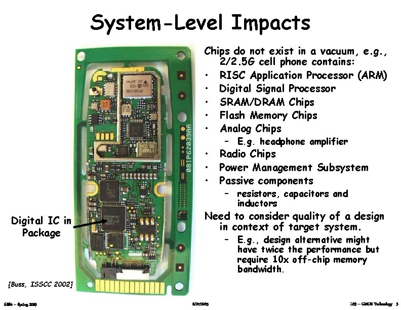
System-Level Impacts Chips do not exist in a vacuum, e. g. , 2/2. 5 G cell phone contains: • RISC Application Processor (ARM) • Digital Signal Processor • SRAM/DRAM Chips • Flash Memory Chips • Analog Chips • • • Digital IC in Package – E. g. headphone amplifier Radio Chips Power Management Subsystem Passive components – resistors, capacitors and inductors Need to consider quality of a design in context of target system. – E. g. , design alternative might have twice the performance but require 10 x off-chip memory bandwidth. [Buss, ISSCC 2002] 6. 884 – Spring 2005 2/07/2005 L 03 – CMOS Technology 3

Digital Technology Generations • • Electromechanical Relays Vacuum Tubes Bipolar Transistors CMOS/FET Transistors • Future: – ~10, 000 nm gates originally, now down to 90 nm in production – scaling will stop somewhere below 30 nm (over 100 billion trans. /chip) – 3 D CMOS (10 trillion transistors/system? ) – Carbon Nanotubes? – Molecular Electronics? CMOS VLSI is the digital implementation technology of choice for the foreseeable future (next 10 -20 years) – Excellent energy versus delay characteristics – High density of wires and transistors – Monolithic manufacturing of devices and interconnect, cheap! 6. 884 – Spring 2005 2/07/2005 L 03 – CMOS Technology 4

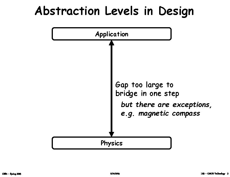
Abstraction Levels in Design Application Gap too large to bridge in one step but there are exceptions, e. g. magnetic compass Physics 6. 884 – Spring 2005 2/07/2005 L 03 – CMOS Technology 5

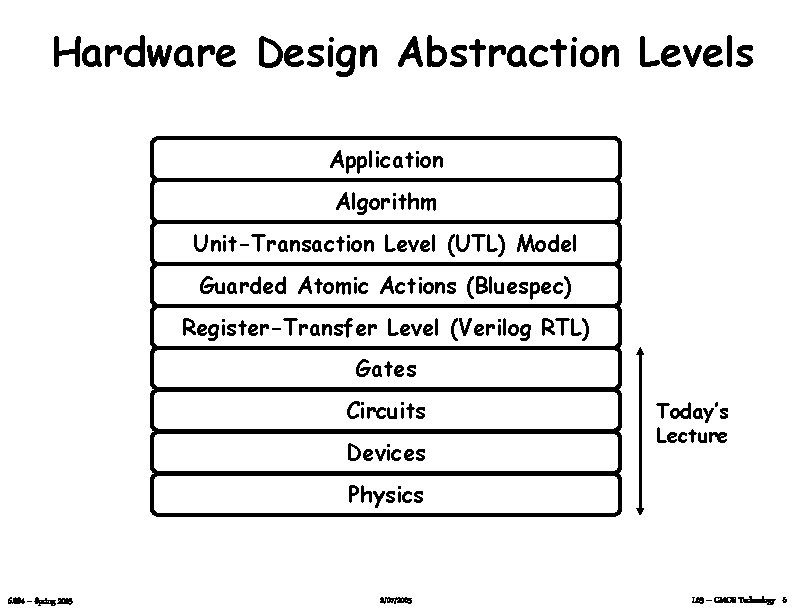
Hardware Design Abstraction Levels Application Algorithm Unit-Transaction Level (UTL) Model Guarded Atomic Actions (Bluespec) Register-Transfer Level (Verilog RTL) Gates Circuits Devices Today’s Lecture Physics 6. 884 – Spring 2005 2/07/2005 L 03 – CMOS Technology 6

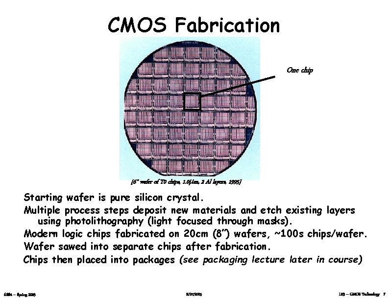
CMOS Fabrication One chip [6” wafer of T 0 chips, 1. 0 mm, 2 Al layers, 1995] Starting wafer is pure silicon crystal. Multiple process steps deposit new materials and etch existing layers using photolithography (light focused through masks). Modern logic chips fabricated on 20 cm (8”) wafers, ~100 s chips/wafer. Wafer sawed into separate chips after fabrication. Chips then placed into packages (see packaging lecture later in course) 6. 884 – Spring 2005 2/07/2005 L 03 – CMOS Technology 7

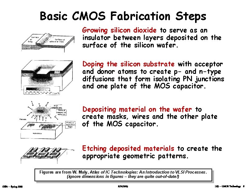
Basic CMOS Fabrication Steps Growing silicon dioxide to serve as an insulator between layers deposited on the surface of the silicon wafer. Doping the silicon substrate with acceptor and donor atoms to create p- and n-type diffusions that form isolating PN junctions and one plate of the MOS capacitor. Depositing material on the wafer to create masks, wires and the other plate of the MOS capacitor. Etching deposited materials to create the appropriate geometric patterns. Figures are from W. Maly, Atlas of IC Technologies: An Introduction to VLSI Processes. (ignore dimensions in figures – they are quite out-of-date!) 6. 884 – Spring 2005 2/07/2005 L 03 – CMOS Technology 8

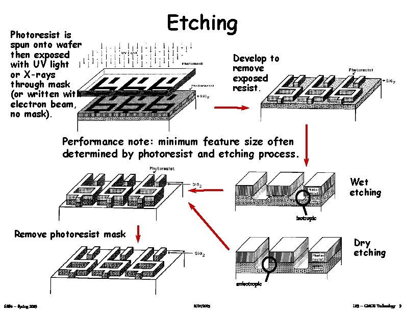
Photoresist is spun onto wafer then exposed with UV light or X-rays through mask (or written with electron beam, no mask). Etching Develop to remove exposed resist. Performance note: minimum feature size often determined by photoresist and etching process. Wet etching isotropic Remove photoresist mask Dry etching anisotropic 6. 884 – Spring 2005 2/07/2005 L 03 – CMOS Technology 9

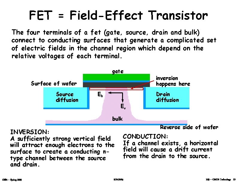
FET = Field-Effect Transistor The four terminals of a fet (gate, source, drain and bulk) connect to conducting surfaces that generate a complicated set of electric fields in the channel region which depend on the relative voltages of each terminal. gate Surface of wafer Source diffusion Eh Ev inversion happens here Drain diffusion bulk INVERSION: A sufficiently strong vertical field will attract enough electrons to the surface to create a conducting ntype channel between the source and drain. 6. 884 – Spring 2005 Reverse side of wafer CONDUCTION: If a channel exists, a horizontal field will cause a drift current from the drain to the source. 2/07/2005 L 03 – CMOS Technology 10

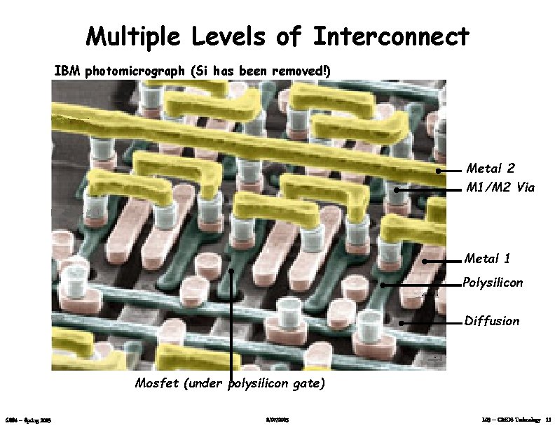
Multiple Levels of Interconnect IBM photomicrograph (Si has been removed!) Metal 2 M 1/M 2 Via Metal 1 Polysilicon Diffusion Mosfet (under polysilicon gate) 6. 884 – Spring 2005 2/07/2005 L 03 – CMOS Technology 11

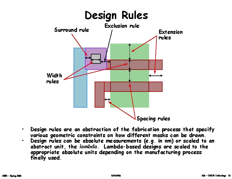
Design Rules Surround rule Exclusion rule Extension rules Width rules Spacing rules • • 6. 884 – Spring 2005 Design rules are an abstraction of the fabrication process that specify various geometric constraints on how different masks can be drawn. Design rules can be absolute measurements (e. g. in nm) or scaled to an abstract unit, the lambda. Lambda-based designs are scaled to the appropriate absolute units depending on the manufacturing process finally used. 2/07/2005 L 03 – CMOS Technology 12

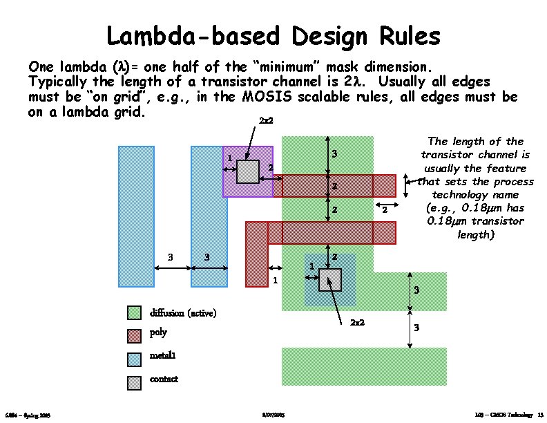
Lambda-based Design Rules One lambda (l)= one half of the “minimum” mask dimension. Typically the length of a transistor channel is 2 l. Usually all edges must be “on grid”, e. g. , in the MOSIS scalable rules, all edges must be on a lambda grid. 2 x 2 1 3 2 2 2 3 3 1 diffusion (active) poly 1 2 The length of the transistor channel is usually the feature that sets the process technology name (e. g. , 0. 18 mm has 0. 18 mm transistor length) 2 3 2 x 2 3 metal 1 contact 6. 884 – Spring 2005 2/07/2005 L 03 – CMOS Technology 13

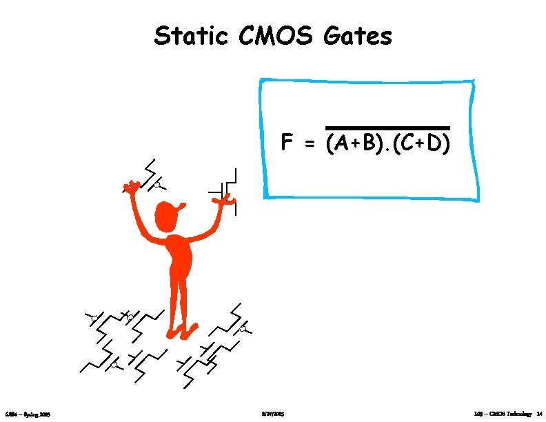
Static CMOS Gates F = (A+B). (C+D) 6. 884 – Spring 2005 2/07/2005 L 03 – CMOS Technology 14

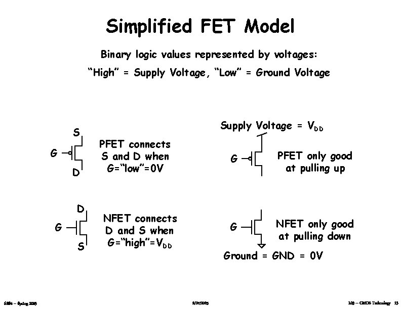
Simplified FET Model Binary logic values represented by voltages: “High” = Supply Voltage, “Low” = Ground Voltage S G D D G S 6. 884 – Spring 2005 Supply Voltage = VDD PFET connects S and D when G=“low”=0 V NFET connects D and S when G=“high”=VDD G PFET only good at pulling up G NFET only good at pulling down Ground = GND = 0 V 2/07/2005 L 03 – CMOS Technology 15

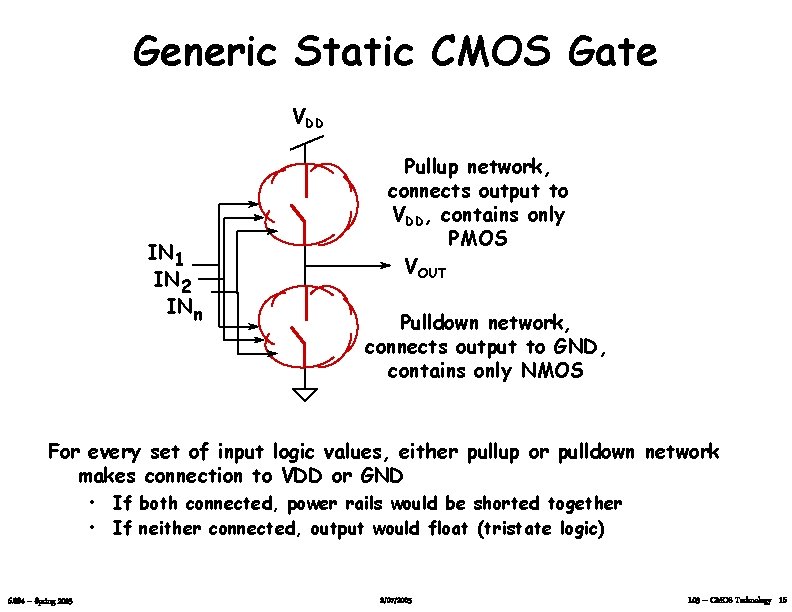
Generic Static CMOS Gate VDD IN 1 IN 2 INn Pullup network, connects output to VDD, contains only PMOS VOUT Pulldown network, connects output to GND, contains only NMOS For every set of input logic values, either pullup or pulldown network makes connection to VDD or GND • If both connected, power rails would be shorted together • If neither connected, output would float (tristate logic) 6. 884 – Spring 2005 2/07/2005 L 03 – CMOS Technology 16

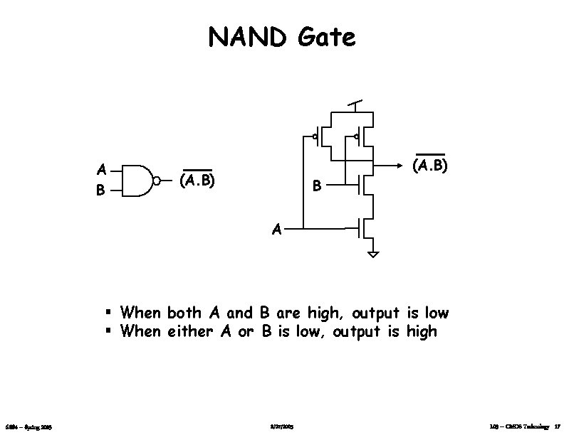
NAND Gate A B (A. B) B A § When both A and B are high, output is low § When either A or B is low, output is high 6. 884 – Spring 2005 2/07/2005 L 03 – CMOS Technology 17

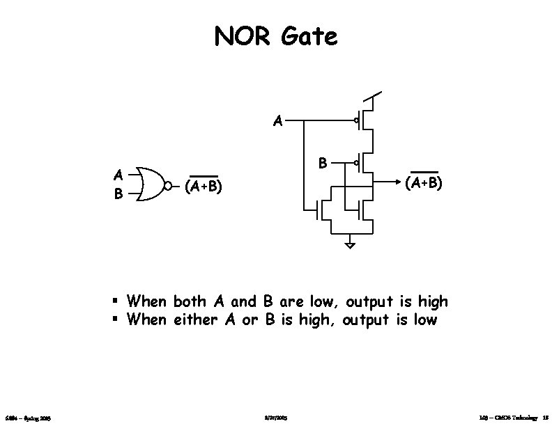
NOR Gate A A B B (A+B) § When both A and B are low, output is high § When either A or B is high, output is low 6. 884 – Spring 2005 2/07/2005 L 03 – CMOS Technology 18

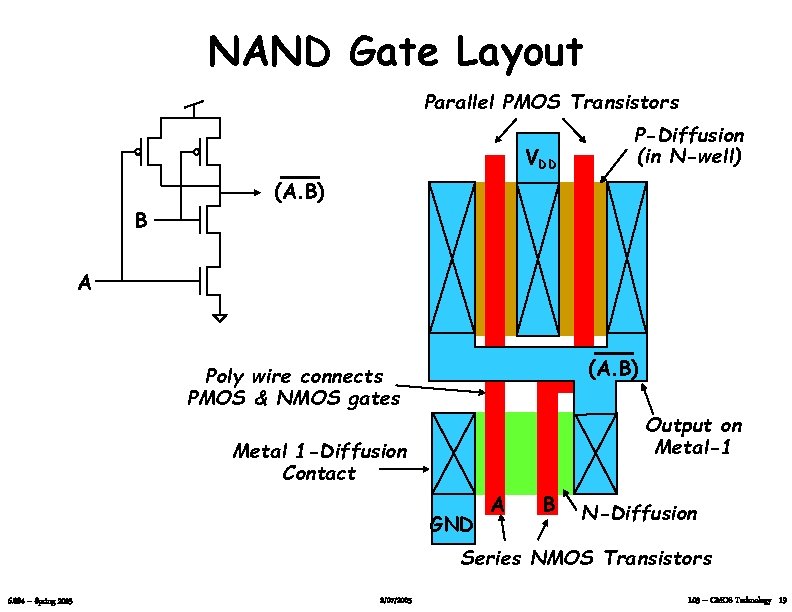
NAND Gate Layout Parallel PMOS Transistors VDD P-Diffusion (in N-well) (A. B) B A (A. B) Poly wire connects PMOS & NMOS gates Output on Metal-1 Metal 1 -Diffusion Contact GND A B N-Diffusion Series NMOS Transistors 6. 884 – Spring 2005 2/07/2005 L 03 – CMOS Technology 19

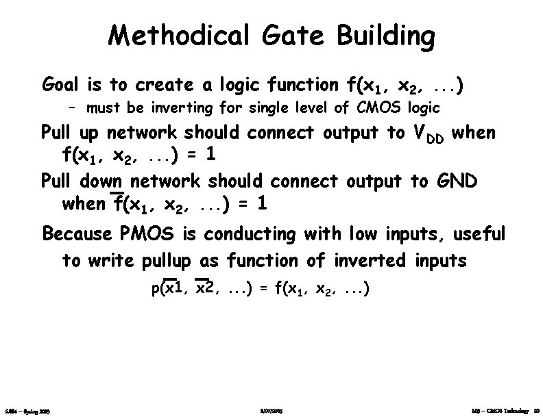
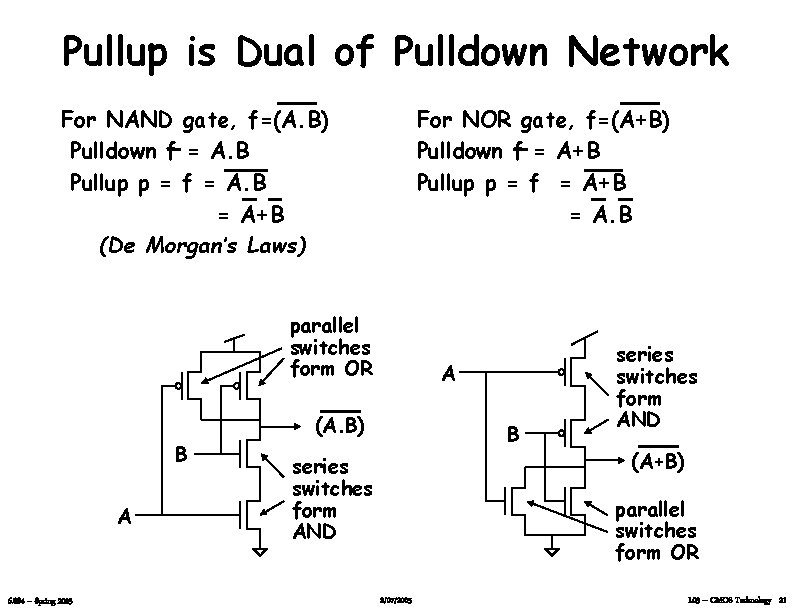
Methodical Gate Building Goal is to create a logic function f(x 1, x 2, . . . ) – must be inverting for single level of CMOS logic Pull up network should connect output to VDD when f(x 1, x 2, . . . ) = 1 Pull down network should connect output to GND when f(x 1, x 2, . . . ) = 1 Because PMOS is conducting with low inputs, useful to write pullup as function of inverted inputs p(x 1, x 2, . . . ) = f(x 1, x 2, . . . ) 6. 884 – Spring 2005 2/07/2005 L 03 – CMOS Technology 20

Pullup is Dual of Pulldown Network For NAND gate, f=(A. B) Pulldown f = A. B Pullup p = f = A. B = A+B (De Morgan’s Laws) For NOR gate, f=(A+B) Pulldown f = A+B Pullup p = f = A+B = A. B parallel switches form OR A (A. B) B A 6. 884 – Spring 2005 B series switches form AND (A+B) parallel switches form OR 2/07/2005 L 03 – CMOS Technology 21

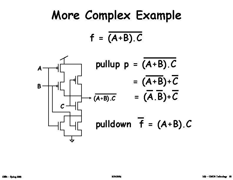
More Complex Example f = (A+B). C A pullup p = (A+B). C B = (A+B)+C C (A+B). C = (A. B)+C pulldown f = (A+B). C 6. 884 – Spring 2005 2/07/2005 L 03 – CMOS Technology 22

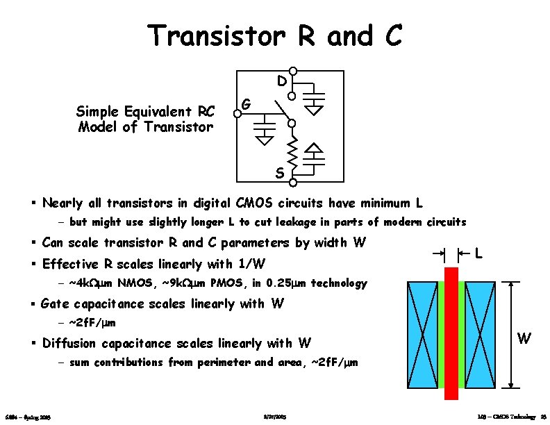
Transistor R and C D Simple Equivalent RC Model of Transistor G S § Nearly all transistors in digital CMOS circuits have minimum L - but might use slightly longer L to cut leakage in parts of modern circuits § Can scale transistor R and C parameters by width W § Effective R scales linearly with 1/W L - ~4 k. Wmm NMOS, ~9 k. Wmm PMOS, in 0. 25 mm technology § Gate capacitance scales linearly with W - ~2 f. F/mm § Diffusion capacitance scales linearly with W W - sum contributions from perimeter and area, ~2 f. F/mm 6. 884 – Spring 2005 2/07/2005 L 03 – CMOS Technology 23

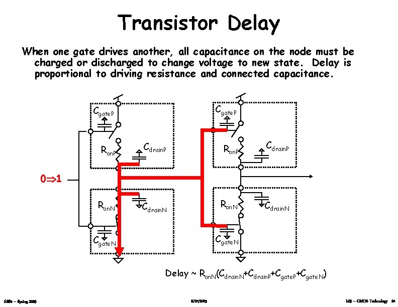
Transistor Delay When one gate drives another, all capacitance on the node must be charged or discharged to change voltage to new state. Delay is proportional to driving resistance and connected capacitance. Cgate. P Ron. P Cdrain. P Ron. N Cdrain. N 0 1 Cgate. N Delay ~ Ron. N(Cdrain. N+Cdrain. P+Cgate. N) 6. 884 – Spring 2005 2/07/2005 L 03 – CMOS Technology 24

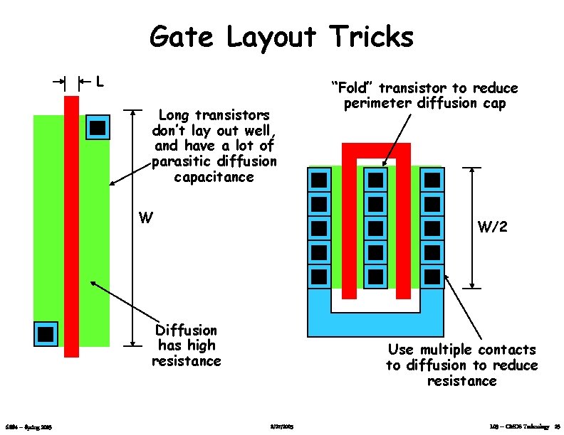
Gate Layout Tricks L Long transistors don’t lay out well, and have a lot of parasitic diffusion capacitance W W/2 Diffusion has high resistance 6. 884 – Spring 2005 “Fold” transistor to reduce perimeter diffusion cap Use multiple contacts to diffusion to reduce resistance 2/07/2005 L 03 – CMOS Technology 25

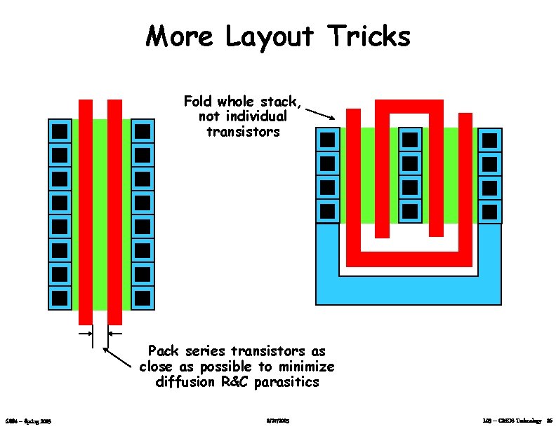
More Layout Tricks Fold whole stack, not individual transistors Pack series transistors as close as possible to minimize diffusion R&C parasitics 6. 884 – Spring 2005 2/07/2005 L 03 – CMOS Technology 26

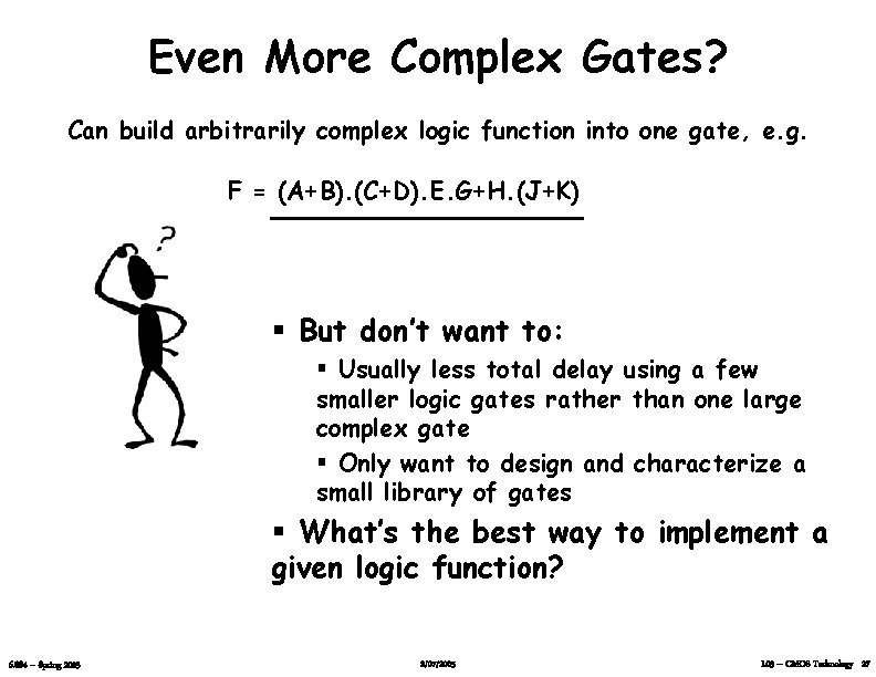
Even More Complex Gates? Can build arbitrarily complex logic function into one gate, e. g. F = (A+B). (C+D). E. G+H. (J+K) § But don’t want to: § Usually less total delay using a few smaller logic gates rather than one large complex gate § Only want to design and characterize a small library of gates § What’s the best way to implement a given logic function? 6. 884 – Spring 2005 2/07/2005 L 03 – CMOS Technology 27

Method of Logical Effort (Sutherland Sproul) • • Easy way to estimate delays in CMOS process. Indicates correct number of logic stages and transistor sizes. Based on simple RC approximations. Useful for back-of-the-envelope circuit design and to give insight into results of synthesis. 6. 884 – Spring 2005 2/07/2005 L 03 – CMOS Technology 28

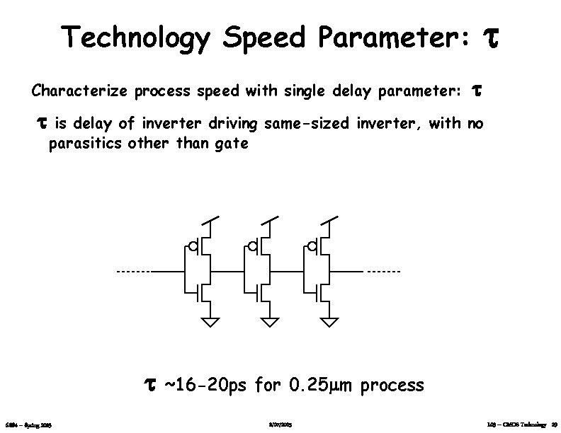
Technology Speed Parameter: Characterize process speed with single delay parameter: is delay of inverter driving same-sized inverter, with no parasitics other than gate 6. 884 – Spring 2005 ~16 -20 ps for 0. 25 mm process 2/07/2005 L 03 – CMOS Technology 29

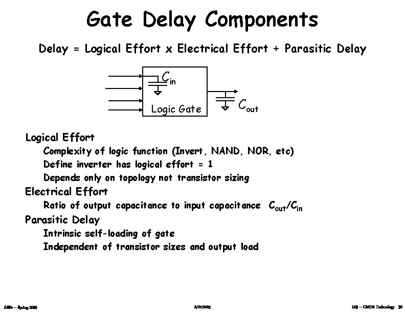
Gate Delay Components Delay = Logical Effort x Electrical Effort + Parasitic Delay Cin Logic Gate Cout Logical Effort Complexity of logic function (Invert, NAND, NOR, etc) Define inverter has logical effort = 1 Depends only on topology not transistor sizing Electrical Effort Ratio of output capacitance to input capacitance Cout/Cin Parasitic Delay Intrinsic self-loading of gate Independent of transistor sizes and output load 6. 884 – Spring 2005 2/07/2005 L 03 – CMOS Technology 30

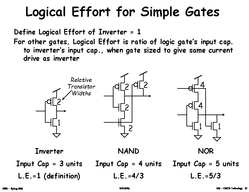
Logical Effort for Simple Gates Define Logical Effort of Inverter = 1 For other gates, Logical Effort is ratio of logic gate’s input cap. to inverter’s input cap. , when gate sized to give same current drive as inverter 2 Relative Transistor Widths 1 2 2 4 4 1 1 Inverter NAND NOR Input Cap = 3 units Input Cap = 4 units Input Cap = 5 units L. E. =1 (definition) L. E. =4/3 L. E. =5/3 6. 884 – Spring 2005 2/07/2005 L 03 – CMOS Technology 31

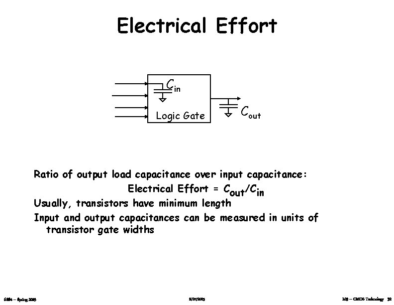
Electrical Effort Cin Logic Gate Cout Ratio of output load capacitance over input capacitance: Electrical Effort = Cout/Cin Usually, transistors have minimum length Input and output capacitances can be measured in units of transistor gate widths 6. 884 – Spring 2005 2/07/2005 L 03 – CMOS Technology 32

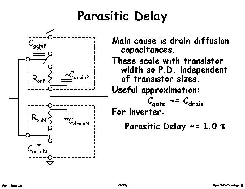
Parasitic Delay Cgate. P Ron. P Cdrain. P Ron. N Cdrain. N Main cause is drain diffusion capacitances. These scale with transistor width so P. D. independent of transistor sizes. Useful approximation: Cgate ~= Cdrain For inverter: Parasitic Delay ~= 1. 0 Cgate. N 6. 884 – Spring 2005 2/07/2005 L 03 – CMOS Technology 33

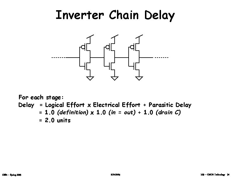
Inverter Chain Delay For each stage: Delay = Logical Effort x Electrical Effort + Parasitic Delay = 1. 0 (definition) x 1. 0 (in = out) + 1. 0 (drain C) = 2. 0 units 6. 884 – Spring 2005 2/07/2005 L 03 – CMOS Technology 34

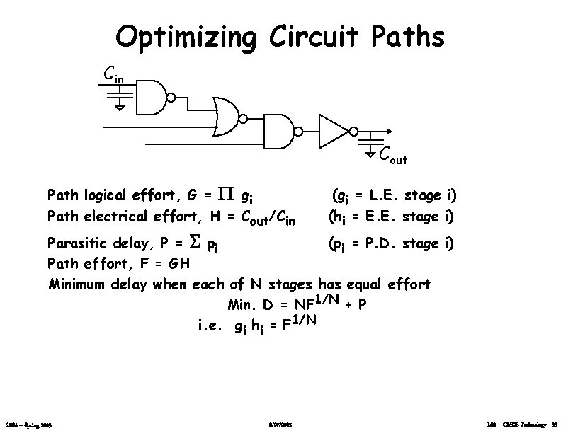
Optimizing Circuit Paths Cin Cout Path logical effort, G = gi Path electrical effort, H = Cout/Cin (gi = L. E. stage i) (hi = E. E. stage i) Parasitic delay, P = pi (pi = P. D. stage i) Path effort, F = GH Minimum delay when each of N stages has equal effort Min. D = NF 1/N + P i. e. gi hi = F 1/N 6. 884 – Spring 2005 2/07/2005 L 03 – CMOS Technology 35

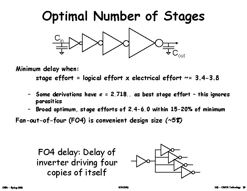
Optimal Number of Stages Cin Cout Minimum delay when: stage effort = logical effort x electrical effort ~= 3. 4 -3. 8 – Some derivations have e = 2. 718. . as best stage effort – this ignores parasitics – Broad optimum, stage efforts of 2. 4 -6. 0 within 15 -20% of minimum t Fan-out-of-four (FO 4) is convenient design size (~5 ) FO 4 delay: Delay of inverter driving four copies of itself 6. 884 – Spring 2005 2/07/2005 L 03 – CMOS Technology 36

Using Logical Effort in Design For given function, pick candidate gate topology Determine optimal stage effort – equal for all stages Starting at last gate – – – output load is known logical effort is known (from gate topology) calculate transistor size to give required stage effort gives output load for preceding stage lather, rinse, repeat. . . Can modify stage efforts up or down to reduce area, power, or to fit fixed set of library cells – optimal sizing has broad optimum In 6. 884, we’ll just let synthesis tool handle gate sizing, but it’s useful to know why the tool makes certain decisions. 6. 884 – Spring 2005 2/07/2005 L 03 – CMOS Technology 37