CMOS Scaling Effects Dr A V N Tilak







- Slides: 43

CMOS Scaling Effects Dr. A. V. N. Tilak Gudlavalleru Engineering College GUDLAVALLERU, A. P.

Outline of my talk 1. Downscaling and it’s possible limit 2. Current downscale scheme and it’s problems 3. Examples of expected difficulties and some solutions 4. Summary and Conclusions

1. Downscaling and it’s possible limit

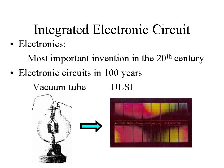
Integrated Electronic Circuit • Electronics: Most important invention in the 20 th century • Electronic circuits in 100 years Vacuum tube ULSI

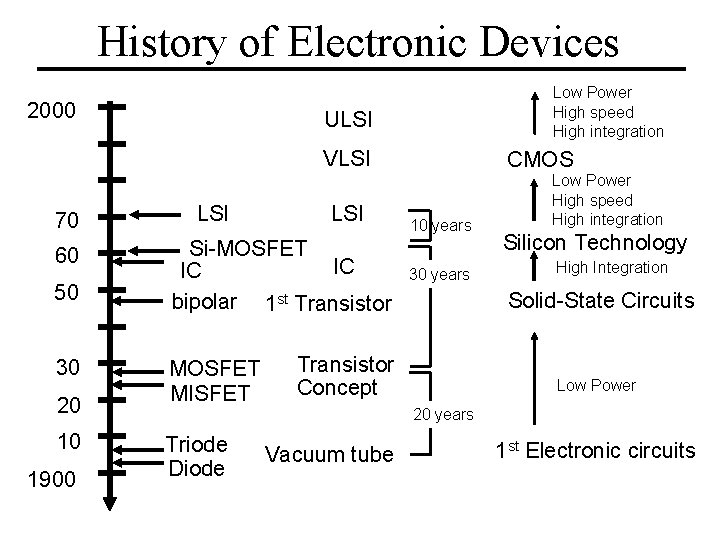
History of Electronic Devices 2000 Low Power High speed High integration ULSI VLSI 70 60 50 30 20 10 1900 LSI Si-MOSFET IC IC bipolar 1 st Transistor MOSFET MISFET CMOS 10 years 30 years Low Power High speed High integration Silicon Technology High Integration Solid-State Circuits Transistor Concept Low Power 20 years Triode Diode Vacuum tube 1 st Electronic circuits

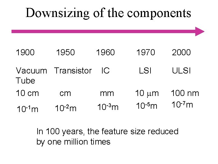
Downsizing of the components 1900 1950 1960 Vacuum Transistor IC Tube 10 cm cm mm 10 -1 m 10 -2 m 10 -3 m 1970 2000 LSI ULSI 10 mm 10 -5 m 100 nm 10 -7 m In 100 years, the feature size reduced by one million times

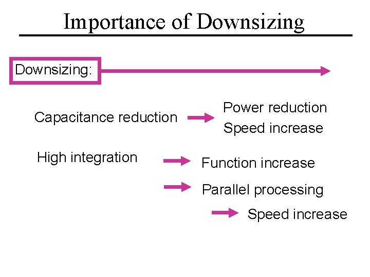
Importance of Downsizing: Capacitance reduction High integration Power reduction Speed increase Function increase Parallel processing Speed increase

Downscaling is important. Then, what will be the limit in downscaling?

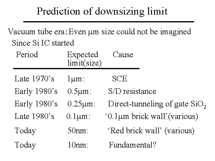
Prediction of downsizing limit Vacuum tube era:Even mm size could not be imagined Since Si IC started Period Expected Cause limit(size) Late 1970’s Early 1980’s Late 1980’s 1 mm: 0. 5 mm: 0. 25 mm: 0. 1 mm: SCE S/D resistance Direct-tunneling of gate Si. O 2 ‘ 0. 1 mm brick wall’(various) Today 50 nm: ‘Red brick wall’ (various) Today 10 nm: Fundamental?

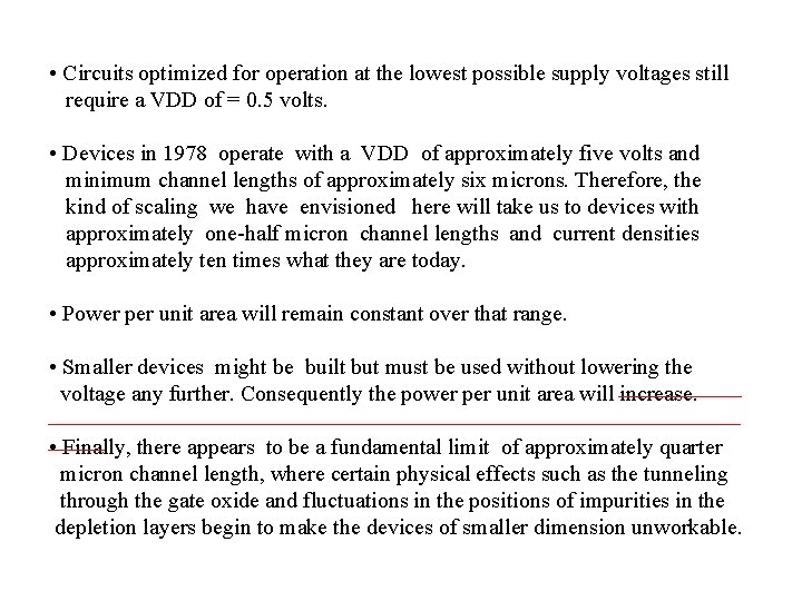
• Circuits optimized for operation at the lowest possible supply voltages still require a VDD of = 0. 5 volts. • Devices in 1978 operate with a VDD of approximately five volts and minimum channel lengths of approximately six microns. Therefore, the kind of scaling we have envisioned here will take us to devices with approximately one-half micron channel lengths and current densities approximately ten times what they are today. • Power per unit area will remain constant over that range. • Smaller devices might be built but must be used without lowering the voltage any further. Consequently the power per unit area will increase. • Finally, there appears to be a fundamental limit of approximately quarter micron channel length, where certain physical effects such as the tunneling through the gate oxide and fluctuations in the positions of impurities in the depletion layers begin to make the devices of smaller dimension unworkable.

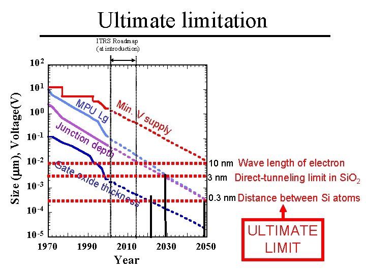
Ultimate limitation ITRS Roadmap (at introduction) Size (mm), Voltage(V) 10 2 10 1 MP 10 -1 10 -2 Ju nc tio Ga 10 -3 nd te o xid Vs up p ly ep th 10 nm Wave length of electron 3 nm Direct-tunneling limit in Si. O 2 e th ick nes 0. 3 nm Distance between Si atoms s 10 -4 10 -5 1970 Min. UL g 10 0 1990 2010 Year 2030 2050 ULTIMATE LIMIT

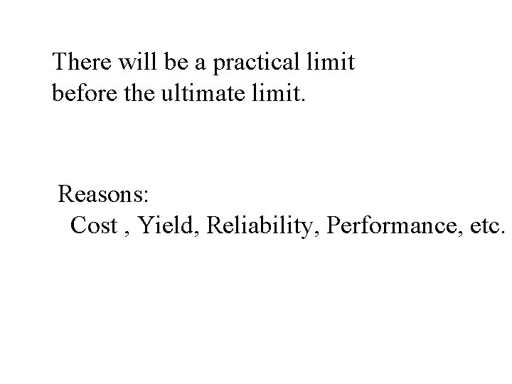
There will be a practical limit before the ultimate limit. Reasons: Cost , Yield, Reliability, Performance, etc.

However, no one knows the practical limit. It is too early to give up.

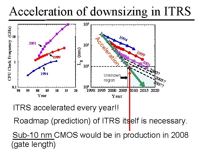
10 3 199 10 1994 0. 1 90 95 00 05 Year 10 1 ion 1 at 1999 ler L g (nm) 10 2 ce 2001 4 Ac CPU Clock Frequency (GHz) Acceleration of downsizing in ITRS 15 20 9 20 01 200 3? 200 5? 7? 10 0 1995 2000 2005 2010 2015 2020 Unknown region 10 199 Year ITRS accelerated every year!! Roadmap (prediction) of ITRS itself is necessary. Sub-10 nm CMOS would be in production in 2008 (gate length)

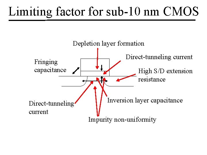
Limiting factor for sub-10 nm CMOS Depletion layer formation Fringing capacitance Direct-tunneling current High S/D extension resistance Inversion layer capacitance Impurity non-uniformity

What is the biggest problem now? Probably, Power increase for a chip operation and Cost increase for next generation lithography including mask making

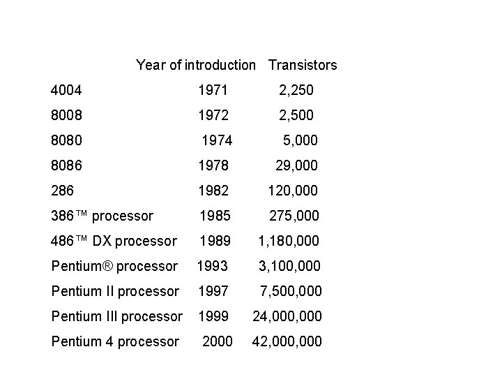
Year of introduction Transistors 4004 1971 2, 250 8008 1972 2, 500 8080 1974 5, 000 8086 1978 29, 000 286 1982 120, 000 386™ processor 1985 275, 000 486™ DX processor 1989 1, 180, 000 Pentium® processor 1993 3, 100, 000 Pentium II processor 1997 7, 500, 000 Pentium III processor 1999 24, 000 Pentium 4 processor 2000 42, 000

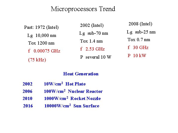
Microprocessors Trend Past: 1972 (Intel) 2008 (Intel) Lg 10, 000 nm Lg sub-70 nm Lg sub-25 nm Tox 1200 nm Tox 1. 4 nm Tox 0. 7 nm f 0. 00075 GHz f 2. 53 GHz f 30 GHz P several 10 W P 10 k. W (75 k. Hz) Heat Generation 2002 10 W/cm 2 Hot Plate 2006 2010 2016 100 W/cm 2 Nuclear Reactor 1000 W/cm 2 Rocket Nozzle 10000 W/cm 2 Sun Surface

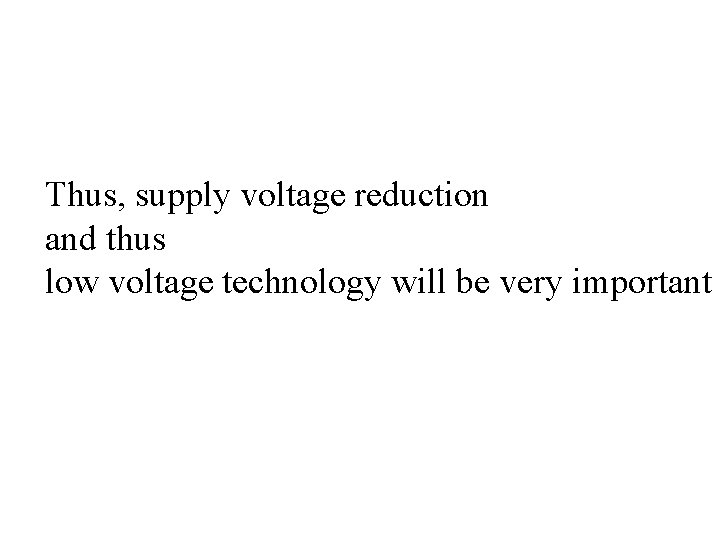
Thus, supply voltage reduction and thus low voltage technology will be very important

2. Current downscale scheme and it’s problems

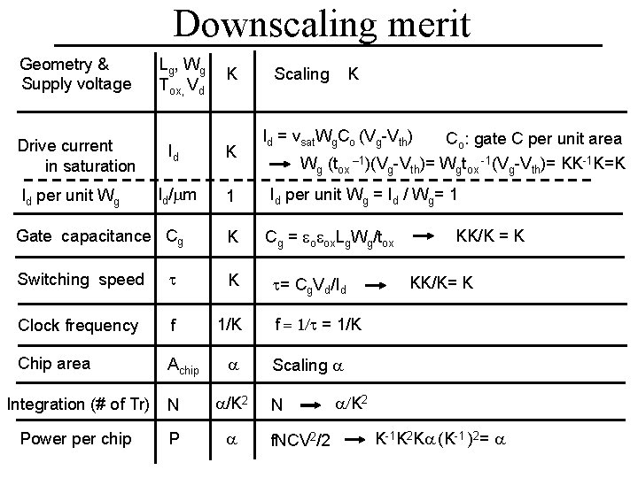
Downscaling merit Geometry & Supply voltage Drive current in saturation Id per unit Wg Lg , W g Tox, Vd K Scaling K Id = vsat. Wg. Co (Vg-Vth) Co: gate C per unit area Wg (tox – 1)(Vg-Vth)= Wgtox -1(Vg-Vth)= KK-1 K=K Id/mm 1 Id per unit Wg = Id / Wg= 1 K Cg = eoeox. Lg. Wg/tox Gate capacitance Cg Switching speed t K Clock frequency f 1/K Chip area Achip a Integration (# of Tr) N a/K 2 Power per chip P a t= Cg. Vd/Id KK/K = K KK/K= K f = 1/t = 1/K Scaling a N f. NCV 2/2 a/K 2 K-1 K 2 Ka (K-1 )2= a

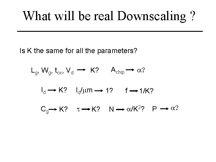
What will be real Downscaling ? Is K the same for all the parameters? K? Lg, Wg, tox, Vd Id K? Id/mm Cg K? t K? a? Achip 1? N f 1/K? a/K 2? P a?

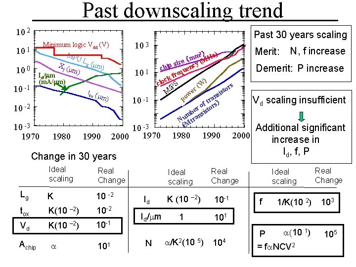
Past downscaling trend 10 2 Past 30 years scaling 10 3 Minimum logic Vdd (V) MPU Lg ( mm) Xj ( mm) Id/mm (m. A/mm) tox ( mm) 10 1 10 0 10 -1 10 -2 10 -3 1970 1980 1990 2) ) m Hz m ( M size cy ( chip uen q e fr ck ) o l c S W s ( IP or r t e s M i w ns a po r t of ors) r be nsist m Nu tra (M 10 -3 1970 2000 1980 1990 2000 Change in 30 years Ideal scaling Real Change Lg K 10 -2 tox K(10 – 2) 10 -2 K(10 – 2) 10 -1 Vd Achip a 101 Ideal scaling Id Id/mm N 10 -1 1 104 N, f increase Demerit: P increase Vd scaling insufficient Additional significant increase in Id, f, P Real Change K (10 – 2) a/K 2(10 5) Merit: Ideal scaling f 1/K(10 2) a(10 1) P = fa. NCV 2 Real Change 103 105

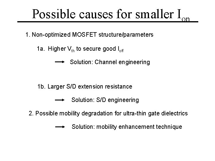
Possible causes for smaller Ion 1. Non-optimized MOSFET structure/parameters 1 a. Higher Vth to secure good Ioff Solution: Channel engineering 1 b. Larger S/D extension resistance Solution: S/D engineering 2. Possible mobility degradation for ultra-thin gate dielectrics Solution: mobility enhancement technique

3. Examples of expected difficulties and some solutions

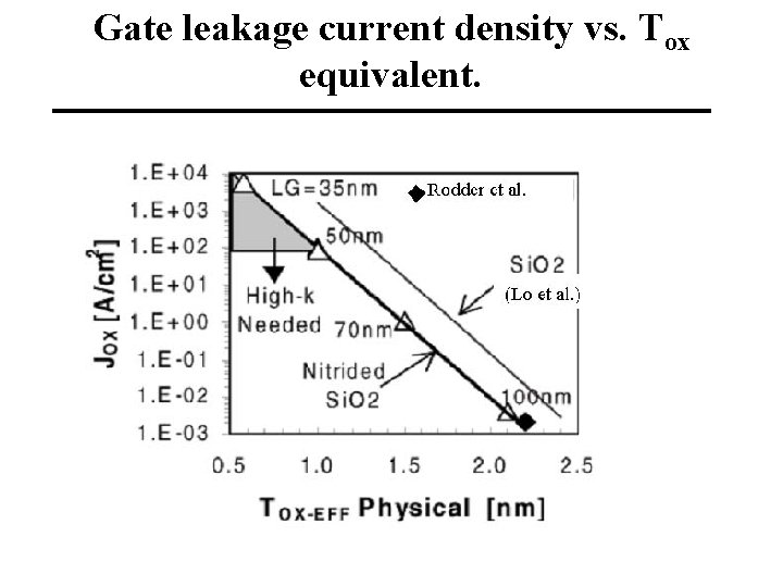
Gate leakage current density vs. Tox equivalent.

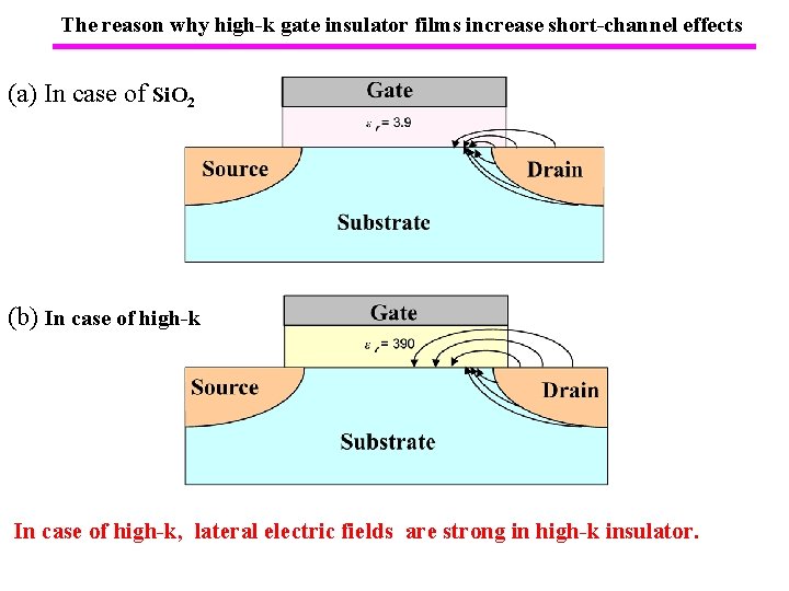
The reason why high-k gate insulator films increase short-channel effects (a) In case of Si. O 2 (b) In case of high-k, lateral electric fields are strong in high-k insulator.

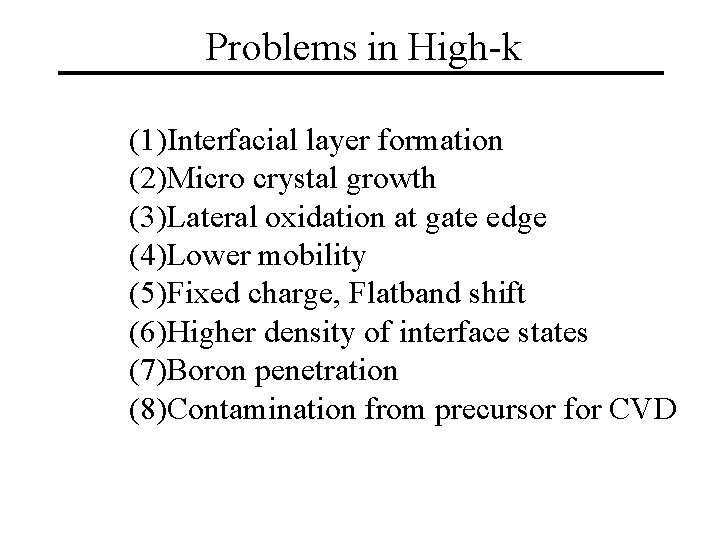
Problems in High-k (1)Interfacial layer formation (2)Micro crystal growth (3)Lateral oxidation at gate edge (4)Lower mobility (5)Fixed charge, Flatband shift (6)Higher density of interface states (7)Boron penetration (8)Contamination from precursor for CVD

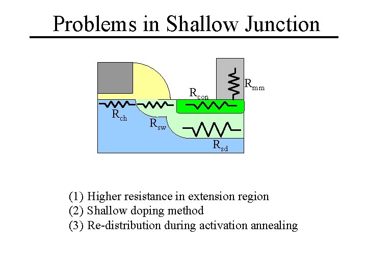
Problems in Shallow Junction Rmm Rcon Rch Rsw Rsd (1) Higher resistance in extension region (2) Shallow doping method (3) Re-distribution during activation annealing

4. Summary and Conclusions

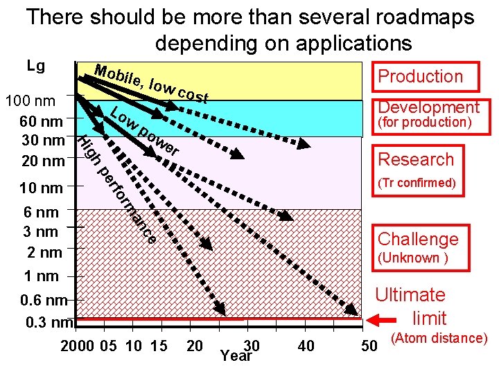
There should be more than several roadmaps depending on applications Lg Lo w Production cost Development (for production) r Research pe (Tr confirmed) an rm rfo Challenge ce 6 nm 3 nm 2 nm gh 10 nm po we Hi 100 nm 60 nm 30 nm 20 nm Mob ile, l ow (Unknown ) 1 nm Ultimate limit 0. 6 nm 0. 3 nm 2000 05 10 15 20 30 Year 40 50 (Atom distance)

Si devices are the smallest devices currently available in the market, and there is no other candidates smaller than Si in future as well. It’s too early to give up silicon device. Problems of downsizing will be solved by introducing new materials, structures, and processes.

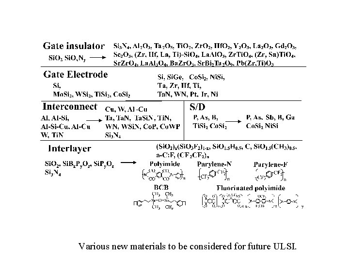
Various new materials to be considered for future ULSI.

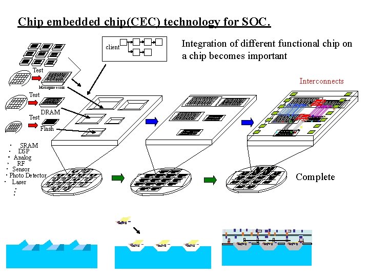
From now, not only the downsizing, but also integration of many different functional subchips on a silicon chip will become very important.

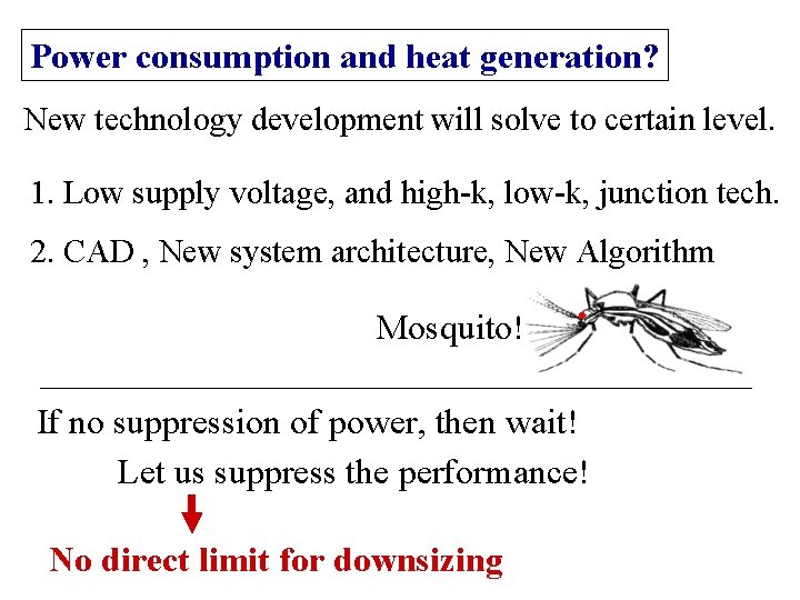
Power consumption and heat generation? New technology development will solve to certain level. 1. Low supply voltage, and high-k, low-k, junction tech. 2. CAD , New system architecture, New Algorithm Mosquito! If no suppression of power, then wait! Let us suppress the performance! No direct limit for downsizing

Cost? Tremendous increase in R&D and production cost. Solution: Alliance between companies for production. Collaboration of industry, academia, government. Resource for Money, Human, Land If no suppression of cost, then wait! Let us suppress the performance and integration! No direct limit for downsizing

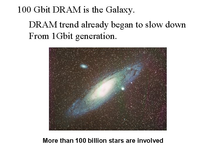
100 Gbit DRAM is the Galaxy. DRAM trend already began to slow down From 1 Gbit generation. More than 100 billion stars are involved

Reliability and Yield? Concerns Particle, defects, Hot carrier effects on Smaller geometry, and thinner film, New material, complicated structure (3 D)? Hard breakdown, or hard failure is reducing for Thinner film, because of tunneling leakage. (bypass) Failsafe design in system side is in progress No direct limit for downsizing

Performance will limit? Maybe or may not be around at 10 nm. If limit in downsizing, Then, consider to increase the performance by other method. Solution: Chip embedded chip (CEC) Tech More intelligent system architecture, algorithm.

Chip embedded chip(CEC) technology for SOC. client Integration of different functional chip on a chip becomes important Test Microprocessor Interconnects Test DRAM Flash SRAM DSP Analog RF Sensor Photo Detector Laser Complete

CMOS is the smallest device among other candidates. Production: Lg = sub 100 nm, tox = 1. 4 nm Research: Lg = 6 nm, tox = 0. 7 nm 30 years ago: Production: tox = 100 nm I have been participate in ‘NANO TECH’ for 30 years, and now move to PICO TECH. If CMOS faces the downsizing limit, other devices will also face the limit at the same size or even larger size.

Lg = 6 nm is the length of only 20 Si atoms Tox = 0. 7 nm is only the length of 2 Si atoms Thus, the downsizing limit is not very far. Regardless of the downsizing limit, Si CMOS will be the main device at least for 50 years. Integration of other functional chips on the Si will be more importnt.

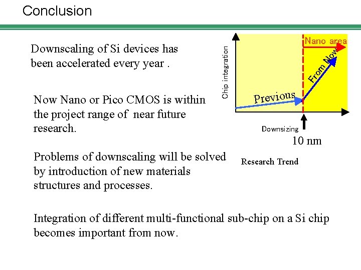
Conclusion Now Nano or Pico CMOS is within the project range of near future research. Problems of downscaling will be solved by introduction of new materials structures and processes. No w om Fr Chip integration Downscaling of Si devices has been accelerated every year. Nano area Previous Downsizing 10 nm Research Trend Integration of different multi-functional sub-chip on a Si chip becomes important from now.