CMOS n IC built on silicon substrate n


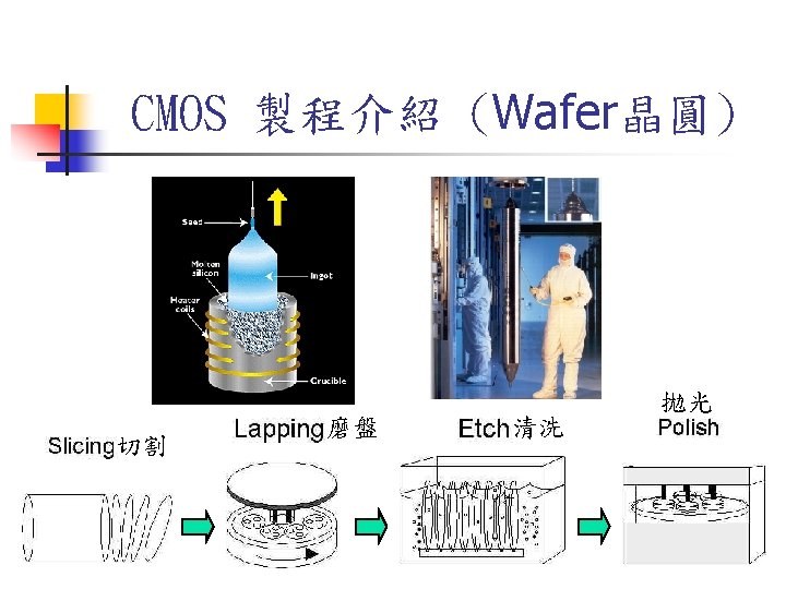
CMOS 製程介紹 n IC built on silicon substrate : n n n some structures diffused into substrate. other structures built on top of substrate. Substrate regions are doped with n-type and p-type impurities. (n+ = heavily doped) Wires made of polycrystalline silicon (poly), multiple layers of aluminum (metal). Insulator - Silicon Dioxide (Si. O 2) n n n Used to insulate transistor gates (thin oxide) Used to insulate layers of wires (field oxide) Can be grown on Silicon or Chemically Deposited

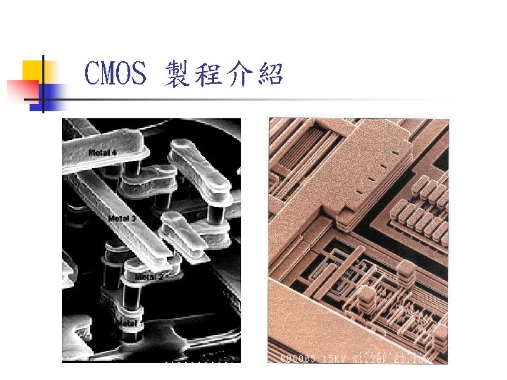
CMOS 製程介紹 n A View of the Cleanroom AMD’s Dresden Fab - Source: AMD Corporation www. amd. com
 n n n Coat wafer with photoresist (PR) Shine UV light")
CMOS 製程介紹 (Photolithography光罩) n n n Coat wafer with photoresist (PR) Shine UV light through mask to selectively expose PR Now use exposed areas for n n Selective doping Selective removal of material under exposed PR UV Light Mask Photoresist Wafer
 poly source/drain gate oxide")
CMOS 製程介紹 (0. 25 micron transistor) poly source/drain gate oxide
")
CMOS 製程介紹 (Example : NOT Gate)
 n")
NOT Gate – Step 1 Form N-Well regions n Grow oxide (長氧化層 ) n Deposit photoresist ( 沈積光阻) oxide p-type substrate Cross section view NWELL mask Layout view photoresist

NOT Gate – Step 1 NWELL mask Form N-Well regions n Grow oxide (長氧化層 ) n n Deposit photoresist ( 沈積光阻) oxide p-type substrate Cross section view Pattern photoresist n n NWELL mask NWELL Mask expose only n-well areas (使用NWELL光罩曝 光產生 作區) Layout view photoresist
 n n")
NOT Gate – Step 1 Form N-Well regions n Etch oxide (去除氧化層) n n Remove photresist ( 移除光阻) n-well p-type substrate Cross section view Diffuse n-type dopants through oxide mask layer (在沒有氧化層的區 域,摻雜n型元素形 成N-Well ) Layout view

NOT Gate – Step 2 ACTIVE mask Form Active Regions n Deposit Si. N over wafer (沈積氮化矽) n Deposit photoresist over Si. N layer (沈積光阻) n-well p-type substrate Si. N photoresist silicon nitride 氮化矽 ACTIVE mask

NOT Gate – Step 2 ACTIVE mask Form Active Regions n Deposit Si. N over wafer (沈積氮化矽) n n Deposit photoresist over Si. N layer (沈積光阻) n-well Si. N photoresist p-type substrate Pattern photoresist n ACTIVE MASK (使用ACTIVE光罩曝 光產生作用區) ACTIVE mask

NOT Gate – Step 2 Form Active Regions n Pattern photoresist n ACTIVE MASK (使用ACTIVE光罩曝 光產生作用區) n n-well Si. N photoresist p-type substrate Etch Si. N in exposed areas n leaves Si. N mask which blocks oxide growth (移除氮化矽準備產 生厚氧化層) ACTIVE mask
 n")
NOT Gate – Step 2 Form Active Regions n Remove photoresist ( 移除光阻) n n Grow Field Oxide FOX (長厚氧化層 ) n-well FOX p-type substrate Remove Si. N (移除氮化矽) ACTIVE mask

NOT Gate – Step 3 Form Gate Poly n Grow thin Gate Oxide (長閘極氧化層 ) POLY mask gate oxide n n Deposit Polysilicon (沈積多晶矽) Deposit Photoresist (沈積光阻) POLY mask polysilicon

NOT Gate – Step 3 Form Gate Poly n Grow thin Gate Oxide (長閘極氧化層 ) n POLY mask gate oxide Pattern Photoresist n POLY MASK (使用POLY 光罩曝 光產生閘極) n Etch Poly in exposed areas (移除多晶矽層) POLY mask

NOT Gate – Step 3 Form Gate Poly n Etch Poly in exposed areas (移除多晶矽層) n Etch Oxide (移除氧化層) gate oxide

NOT Gate – Step 4 PSELECT mask Form pmos S/D n Deposit photoresist ( 沈積光阻) n Pattern photoresist n PSELECT MASK (使用PSELECT光罩 曝光產生PMOS的 源極與汲極) PSELECT mask

NOT Gate – Step 4 PSELECT mask Form pmos S/D n Pattern photoresist n PSELECT MASK (使用PSELECT光罩 曝光產生PMOS的 源極與汲極) n Remove photoresist (移除光阻) POLY mask
 n")
NOT Gate – Step 4 Form pmos S/D n Implant p-type dopants (植入P型元素) n p+ dopant Remove photoresist ( 移除光阻) POLY mask

NOT Gate – Step 5 NSELECT mask Form nmos S/D n Deposit photoresist ( 沈積光阻) n p+ p+ p+ n Pattern photoresist n NSELECT MASK (使用NSELECT光罩 曝光產生NMOS的 源極與汲極) POLY mask

NOT Gate – Step 5 NSELECT mask Form nmos S/D n Pattern photoresist n NSELECT MASK (使用NSELECT光罩 曝光產生NMOS的 源極與汲極) n p+ p+ p+ n Remove photoresist (移除光阻) POLY mask
 n")
NOT Gate – Step 5 Form nmos S/D n Implant n-type dopants (植入N型元素) n n+ p+ p+ n+ n+ n n+ dopant Remove photoresist ( 移除光阻) POLY mask p+
 n")
NOT Gate – Step 6 CONTACT mask Form Contacts n Deposit oxide (沈積氧化層) n n+ p+ n Deposit photoresist (沈積光阻) CONTACT mask p+ n+ n+ p+

NOT Gate – Step 6 CONTACT mask Form Contacts n Pattern photoresist n CONTACT Mask (使用CONTACT光罩 曝光產生active層與 poly層之連接點) n+ p+ n CONTACT mask p+ n+ n+ p+

NOT Gate – Step 6 Form Contacts n Pattern photoresist n CONTACT Mask (使用CONTACT光罩 曝光產生active層與 poly層之連接點) n Etch oxide (移除氧化層) n+ n p+ p+ n+ n+ p+
 n n Deposit")
NOT Gate – Step 6 Form Contacts n Remove photoresist (移除光阻) n n Deposit metal 1 (沈積第一金屬層) Planerize (磨平第一金屬層) n+ n p+ p+ n+ n+ p+

NOT Gate – Step 7 METAL 1 mask Form Metal 1 Traces n Deposit photoresist (沈積光阻) n n+ p+ p+ n+ n Pattern photoresist n METAL 1 Mask (使用METAL 1光罩 曝光產生連接線路) METAL 1 mask n+ p+

NOT Gate – Step 7 Form Metal 1 Traces n Pattern photoresist n METAL 1 Mask (使用METAL 1光罩 曝光產生連接線路) n Etch metal (移除第一金屬層) n+ p+ p+ n+ n+ p+ n metal over poly outside of cross section

NOT Gate – Step 7 Form Metal 1 Traces n Pattern photoresist n METAL 1 Mask (使用METAL 1光罩 曝光產生連接線路) n n Etch metal (移除第一金屬層) Remove photoresist (移除光阻) n+ n p+ p+ n+ n+ p+

NOT Gate – Step 8 VIA mask Form Vias to Metal 1 n Deposit oxide (沈積氧化層) n n n+ p+ p+ n Planerize oxide (磨平氧化層) Deposit photoresist (沈積光阻) VIA mask n+ n+ p+

NOT Gate – Step 8 VIA mask Form Vias to Metal 1 n Deposit photoresist (沈積光阻) n n+ p+ p+ n Pattern photoresist n VIA Mask (使用VIA光罩曝光產 生連接金屬層之貫 孔) VIA mask n+ n+ p+

NOT Gate – Step 8 Form Vias to Metal 1 n Pattern photoresist n VIA Mask (使用VIA光罩曝光產 生連接金屬層之貫 孔) n n Etch oxide (移除氧化層) Remove photoresist (移除光阻) n+ n p+ p+ n+ n+ p+

NOT Gate – Step 8 Form Vias to Metal 1 n Deposit Metal 2 (沈積第二金屬層) n+ n p+ p+ n+ n+ p+

NOT Gate – Step 9 METAL 2 mask Form Metal 2 Traces n Deposit photoresist (沈積光阻) n+ n n Pattern photoresist n METAL 2 Mask (使用METAL 2光罩 曝光產生連接線路) p+ p+ n+ n+ p+

NOT Gate – Step 9 Form Metal 2 Traces n Pattern photoresist METAL 2 Mask n+ (使用METAL 2光罩 曝光產生連接線路) n n n Etch metal (移除第二金屬層) p+ p+ n+ n+ p+

NOT Gate – Step 9 Form Metal 2 Traces n Pattern photoresist METAL 2 Mask n+ (使用METAL 2光罩 曝光產生連接線路) n n Etch metal (移除第二金屬層) Remove photoresist (移除光阻) p+ p+ n+ n+ p+

NOT Gate – Step 10+ Form Additional Traces n Deposit oxide n Deposit photoresist n Pattern photoresist n Etch oxide n Deposit metal n Deposit photresist n Pattern photoresist n Etch metal n Repeat for each additional metal n+ p+ n p-type substrate p+ n+ n+ p+
- Slides: 40