CMOS Logic Gates NMOS transistor acts as a




- Slides: 20

CMOS Logic Gates

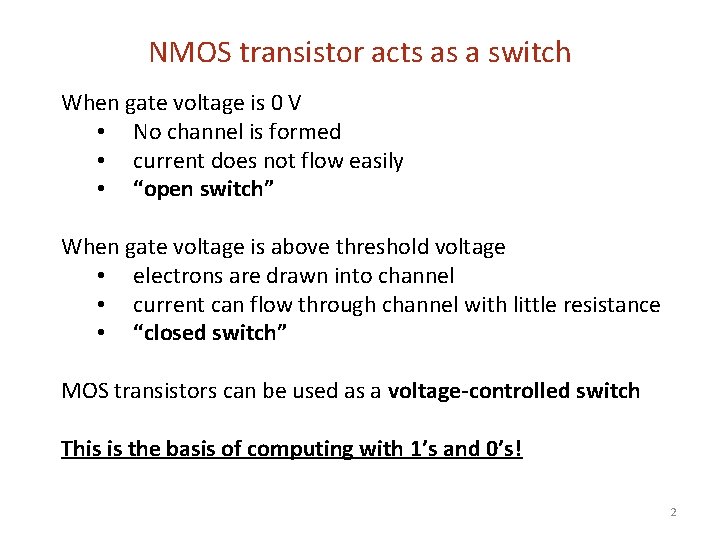
NMOS transistor acts as a switch When gate voltage is 0 V • No channel is formed • current does not flow easily • “open switch” When gate voltage is above threshold voltage • electrons are drawn into channel • current can flow through channel with little resistance • “closed switch” MOS transistors can be used as a voltage-controlled switch This is the basis of computing with 1’s and 0’s! 2

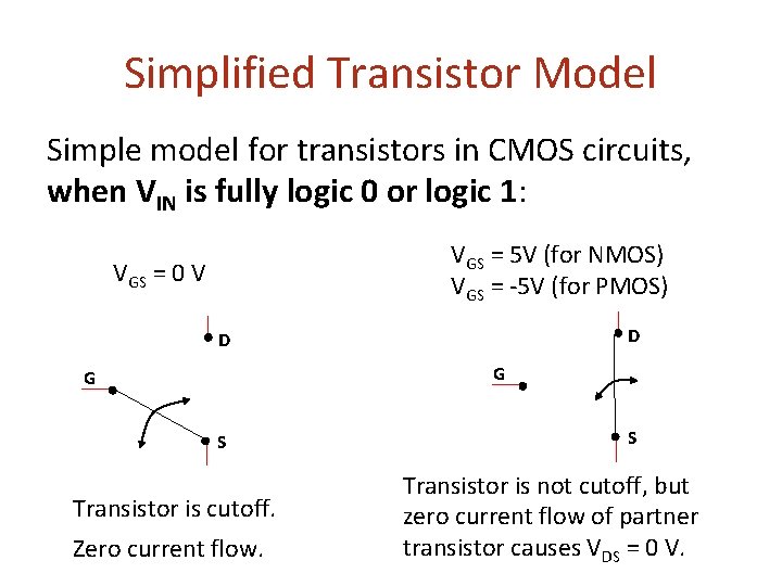
Simplified Transistor Model Simple model for transistors in CMOS circuits, when VIN is fully logic 0 or logic 1: VGS = 5 V (for NMOS) VGS = -5 V (for PMOS) VGS = 0 V D D G G S Transistor is cutoff. Zero current flow. S Transistor is not cutoff, but zero current flow of partner transistor causes VDS = 0 V.

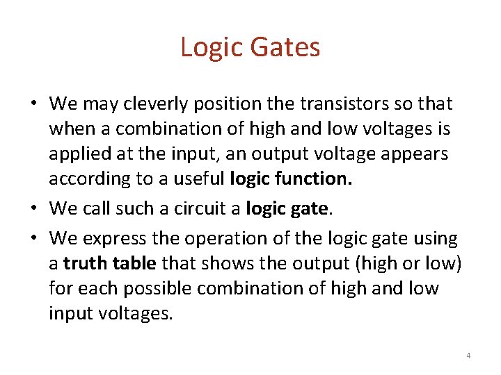
Logic Gates • We may cleverly position the transistors so that when a combination of high and low voltages is applied at the input, an output voltage appears according to a useful logic function. • We call such a circuit a logic gate. • We express the operation of the logic gate using a truth table that shows the output (high or low) for each possible combination of high and low input voltages. 4

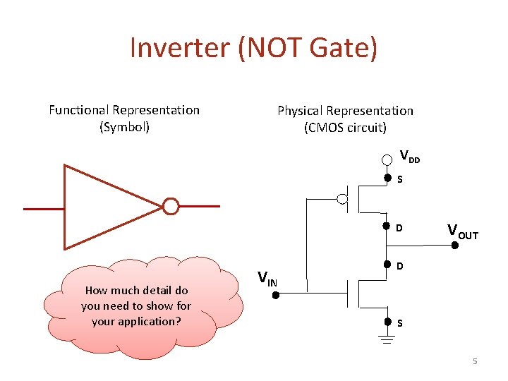
Inverter (NOT Gate) Functional Representation (Symbol) Physical Representation (CMOS circuit) VDD S D How much detail do you need to show for your application? VIN VOUT D S 5

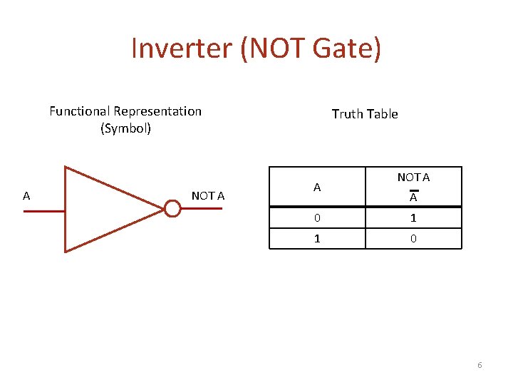
Inverter (NOT Gate) Functional Representation (Symbol) A NOT A Truth Table A NOT A A 0 1 1 0 6

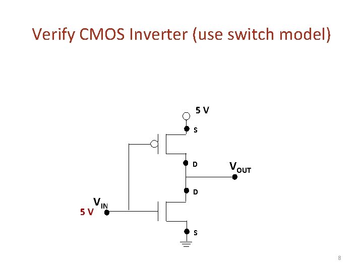
Verify CMOS Inverter (use switch model) 5 V S D VIN VOUT D 0 V S 7

Verify CMOS Inverter (use switch model) 5 V S D VIN VOUT D 5 V S 8

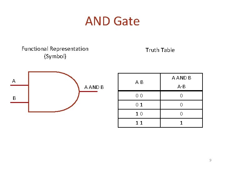
AND Gate Functional Representation (Symbol) A B A AND B Truth Table AB A AND B A·B 00 0 01 0 10 0 11 1 9

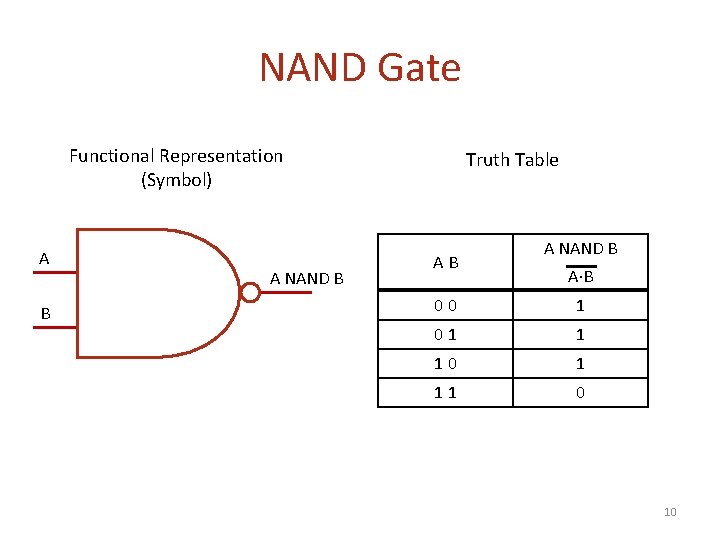
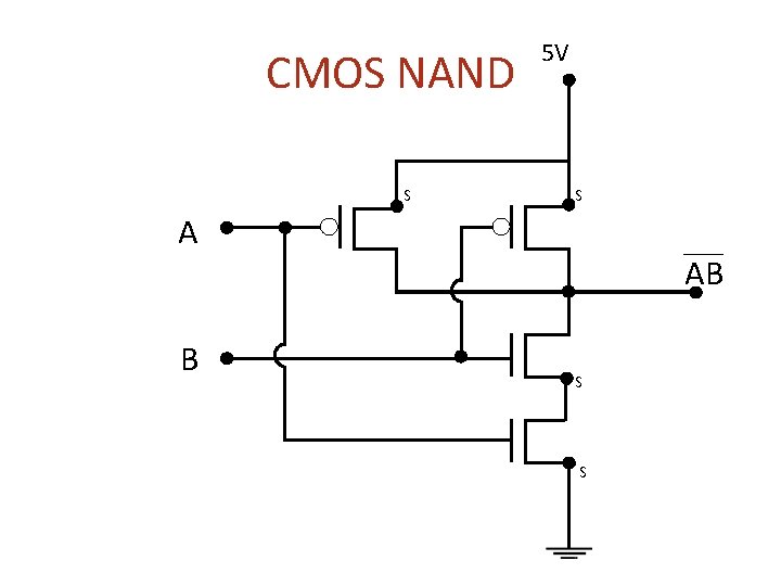
NAND Gate Functional Representation (Symbol) A B A NAND B Truth Table AB A NAND B A·B 00 1 01 1 10 1 11 0 10

CMOS NAND S 5 V S A B AB S S

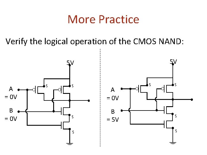
More Practice Verify the logical operation of the CMOS NAND: 5 V 5 V A = 0 V B = 0 V S S A = 0 V B = 5 V S S

More Practice Verify the logical operation of the CMOS NAND: 5 V 5 V A = 5 V B = 0 V S S A = 5 V B = 5 V S S

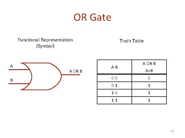
OR Gate Functional Representation (Symbol) A B A OR B Truth Table AB A OR B A+B 00 0 01 1 10 1 11 1 14

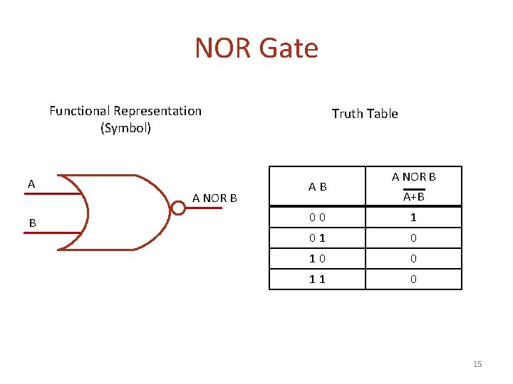
NOR Gate Functional Representation (Symbol) A B A NOR B Truth Table AB A NOR B A+B 00 1 01 0 10 0 11 0 15

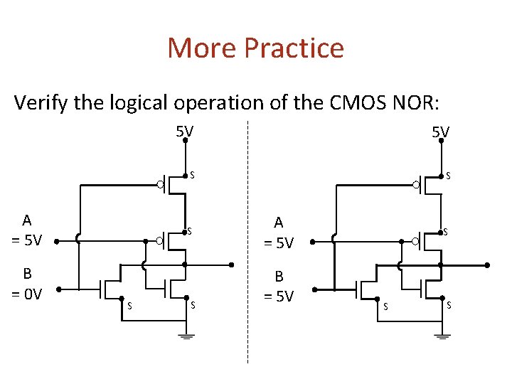
More Practice Verify the logical operation of the CMOS NOR: A = 0 V B = 0 V 5 V 5 V S S S A = 0 V B = 5 V S S S

More Practice Verify the logical operation of the CMOS NOR: A = 5 V B = 0 V 5 V 5 V S S S A = 5 V B = 5 V S S S

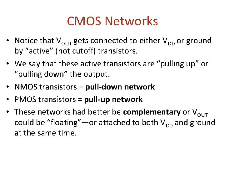
CMOS Networks • Notice that VOUT gets connected to either VDD or ground by “active” (not cutoff) transistors. • We say that these active transistors are “pulling up” or “pulling down” the output. • NMOS transistors = pull-down network • PMOS transistors = pull-up network • These networks had better be complementary or VOUT could be “floating”—or attached to both VDD and ground at the same time.

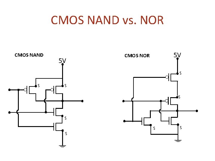
CMOS NAND vs. NOR CMOS NAND 5 V 5 V CMOS NOR S S S S

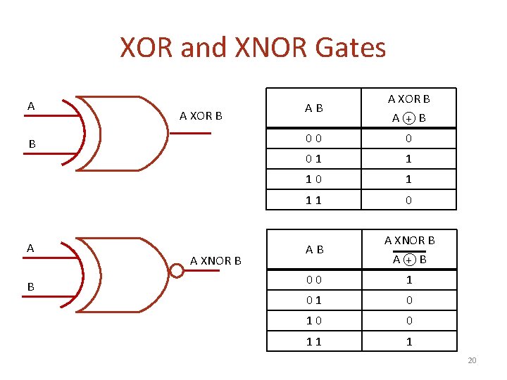
XOR and XNOR Gates A A XOR B B A XNOR B AB A XOR B A + B 00 0 01 1 10 1 11 0 AB A XNOR B A + B 00 1 01 0 10 0 11 1 20