CMOS Logic Gates a delay model Introducing logical



- Slides: 52

CMOS Logic Gates a delay model Introducing logical effort Lecture 5

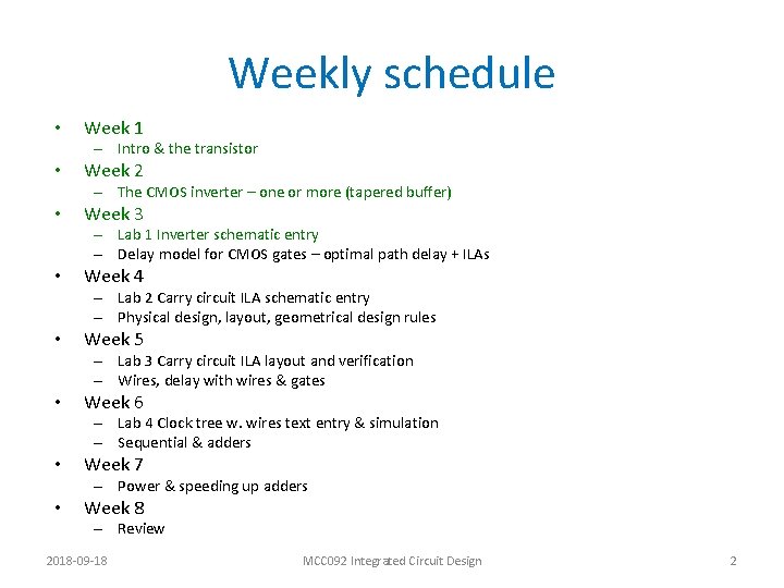
Weekly schedule • Week 1 – Intro & the transistor • Week 2 – The CMOS inverter – one or more (tapered buffer) • Week 3 – Lab 1 Inverter schematic entry – Delay model for CMOS gates – optimal path delay + ILAs • Week 4 – Lab 2 Carry circuit ILA schematic entry – Physical design, layout, geometrical design rules • Week 5 – Lab 3 Carry circuit ILA layout and verification – Wires, delay with wires & gates • Week 6 – Lab 4 Clock tree w. wires text entry & simulation – Sequential & adders • Week 7 – Power & speeding up adders • Week 8 – Review 2018 -09 -18 MCC 092 Integrated Circuit Design 2

Week 3 • Monday lab 1 – CMOS inverter static and dynamic • Tuesday – Lecture Delay with gates, logical effort – Postlab review lab 1 • Thursday – Prelab 2, Lecture on optimal path delay – Tutorial POTW (Victor) • Friday Deadline prelab 2 – – Schematic entry of carry ckt of full adder 2018 -09 -18 MCC 092 Integrated Circuit Design 3

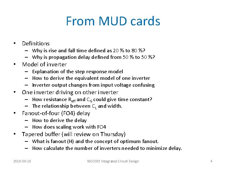
From MUD cards • Definitions – Why is rise and fall time defined as 20 % to 80 %? – Why is propagation delay defined from 50 % to 50 %? • Model of inverter – Explanation of the step response model – How to derive the equivalent model of one inverter – Inverter output changes from input voltage confusing • One inverter driving on other inverter – How resistance Reff and CG could give time constant? – The relationship between CL and width. • Fanout-of-four (FO 4) delay – How to derive the delay – How does scaling work with FO 4 • Tapered buffer (will review on Thursday) – What is fanout (H) and the concept of optimum fanout. – How calculate the number of inverters needed to minimize delay. 2018 -09 -18 MCC 092 Integrated Circuit Design 4

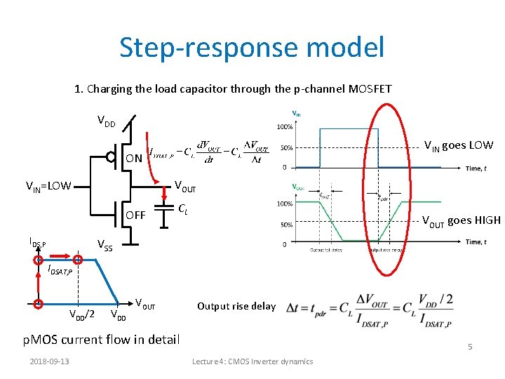
Step-response model 1. Charging the load capacitor through the p-channel MOSFET VDD VIN goes LOW ON VIN=LOW VOUT OFF IDS, P CL VOUT goes HIGH VSS IDSAT, P VDD/2 VDD VOUT Output rise delay p. MOS current flow in detail 2018 -09 -13 5 Lecture 4: CMOS Inverter dynamics

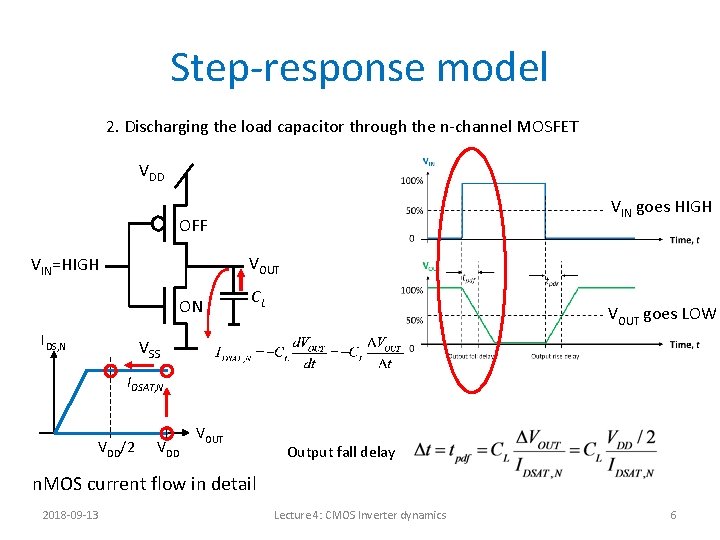
Step-response model 2. Discharging the load capacitor through the n-channel MOSFET VDD VIN goes HIGH OFF VIN=HIGH VOUT ON IDS, N CL VOUT goes LOW VSS IDSAT, N VDD/2 VDD VOUT Output fall delay n. MOS current flow in detail 2018 -09 -13 Lecture 4: CMOS Inverter dynamics 6

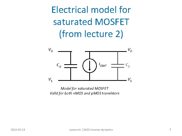
Electrical model for saturated MOSFET (from lecture 2) VG VD CG IDSAT VS CD VS Model for saturated MOSFET Valid for both n. MOS and p. MOS transistors 2018 -09 -13 Lecture 4: CMOS Inverter dynamics 7

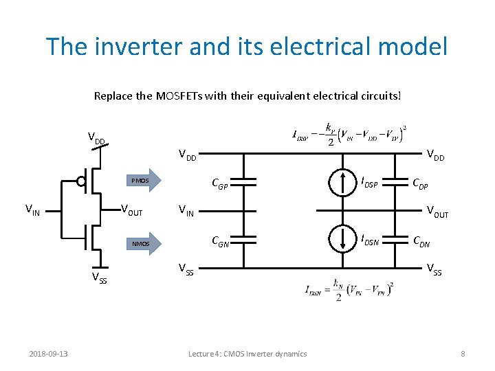
The inverter and its electrical model Replace the MOSFETs with their equivalent electrical circuits! VDD CGP PMOS VIN VOUT 2018 -09 -13 IDSP VIN CDP VOUT CGN NMOS VSS VDD VSS Lecture 4: CMOS Inverter dynamics IDSN CDN VSS 8

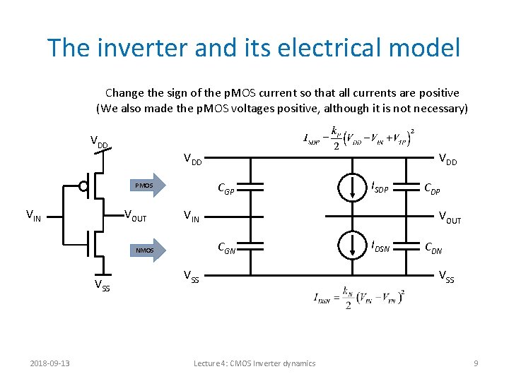
The inverter and its electrical model Change the sign of the p. MOS current so that all currents are positive (We also made the p. MOS voltages positive, although it is not necessary) VDD CGP PMOS VIN VOUT 2018 -09 -13 ISDP VIN CDP VOUT CGN NMOS VSS VDD VSS Lecture 4: CMOS Inverter dynamics IDSN CDN VSS 9

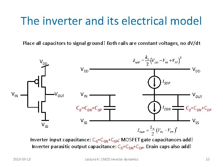
The inverter and its electrical model Place all capacitors to signal ground! Both rails are constant voltages, no d. V/dt VDD VDD ISDP VIN VOUT VIN CG=CGN+CGP VSS VOUT IDSN CD=CDN+CDP VSS Inverter input capacitance: CG=CGN+CGP; MOSFET gate capacitances add! Inverter parasitic output capacitance: CD=CDN+CDP. Drain caps also add! 2018 -09 -13 Lecture 4: CMOS Inverter dynamics 10

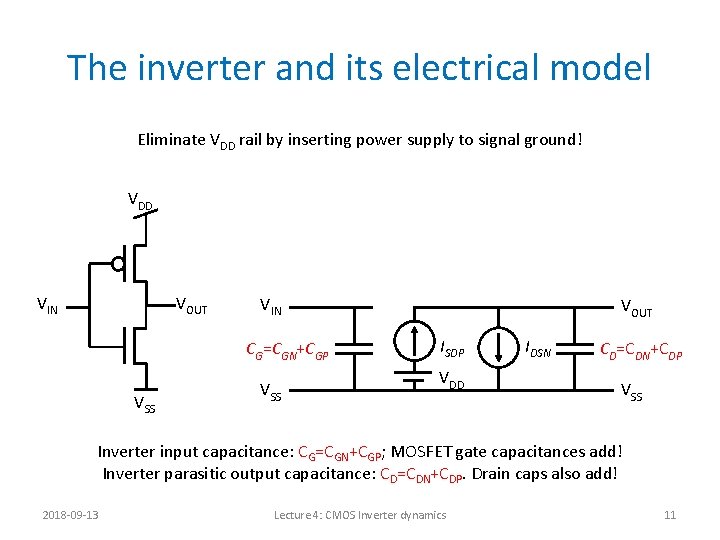
The inverter and its electrical model Eliminate VDD rail by inserting power supply to signal ground! VDD VIN VOUT VIN CG=CGN+CGP VSS VOUT ISDP VDD IDSN CD=CDN+CDP VSS Inverter input capacitance: CG=CGN+CGP; MOSFET gate capacitances add! Inverter parasitic output capacitance: CD=CDN+CDP. Drain caps also add! 2018 -09 -13 Lecture 4: CMOS Inverter dynamics 11

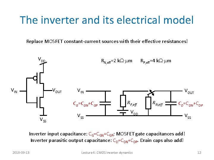
The inverter and its electrical model Replace MOSFET constant-current sources with their effective resistances! VDD VIN RN, eff=2 k. W. mm VOUT VIN CG=CGN+CGP VSS RP, eff=4 k. W. mm VSS VOUT RP, eff VDD RN, eff CD=CDN+CDP VSS Inverter input capacitance: CG=CGN+CGP; MOSFET gate capacitances add! Inverter parasitic output capacitance: CD=CDN+CDP. Drain caps also add! 2018 -09 -13 Lecture 4: CMOS Inverter dynamics 12

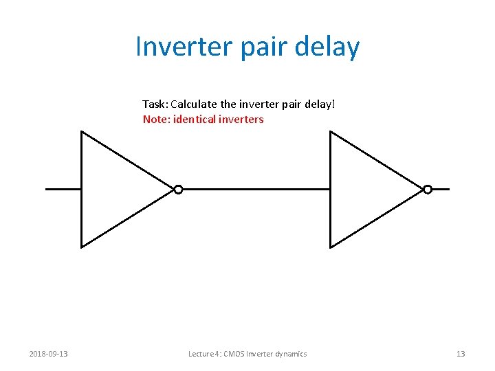
Inverter pair delay Task: Calculate the inverter pair delay! Note: identical inverters VDD Reff 2018 -09 -13 Lecture 4: CMOS Inverter dynamics 13

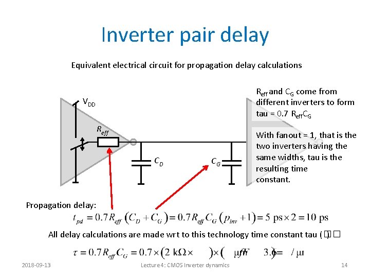
Inverter pair delay Equivalent electrical circuit for propagation delay calculations Reff and CG come from different inverters to form tau = 0. 7 Reff. CG VDD Reff CD CG With fanout = 1, that is the two inverters having the same widths, tau is the resulting time constant. Propagation delay: All delay calculations are made wrt to this technology time constant tau (�� ) 2018 -09 -13 Lecture 4: CMOS Inverter dynamics 14

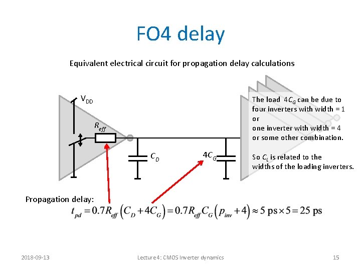
FO 4 delay Equivalent electrical circuit for propagation delay calculations VDD The load 4 CG can be due to four inverters with width = 1 or one inverter with width = 4 or some other combination. Reff CD 4 CG So CL is related to the widths of the loading inverters. Propagation delay: 2018 -09 -13 Lecture 4: CMOS Inverter dynamics 15

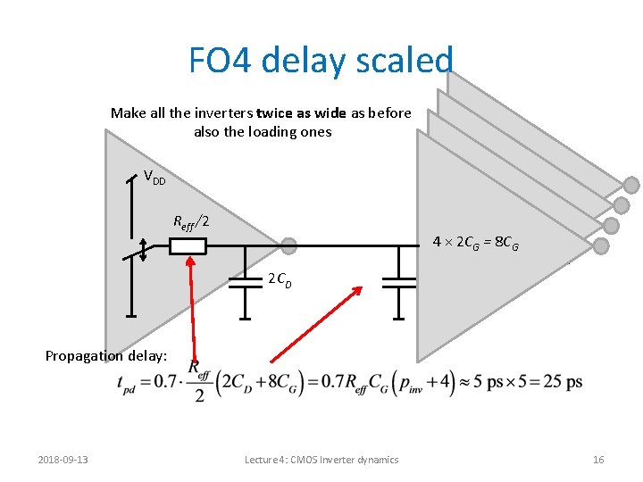
FO 4 delay scaled Make all the inverters twice as wide as before also the loading ones VDD Reff /2 4 × 2 CG = 8 CG 2 CD Propagation delay: 2018 -09 -13 Lecture 4: CMOS Inverter dynamics 16

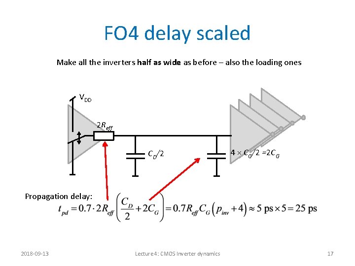
FO 4 delay scaled Make all the inverters half as wide as before – also the loading ones VDD 2 Reff CD/2 4 × CG/2 =2 CG Propagation delay: 2018 -09 -13 Lecture 4: CMOS Inverter dynamics 17

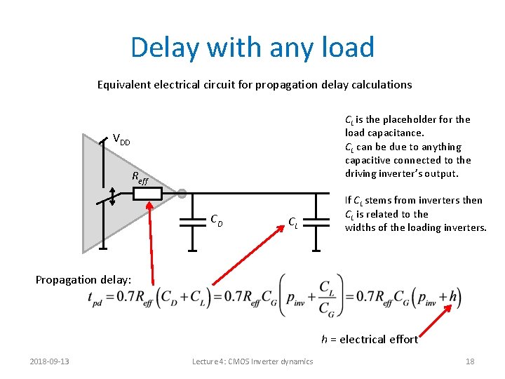
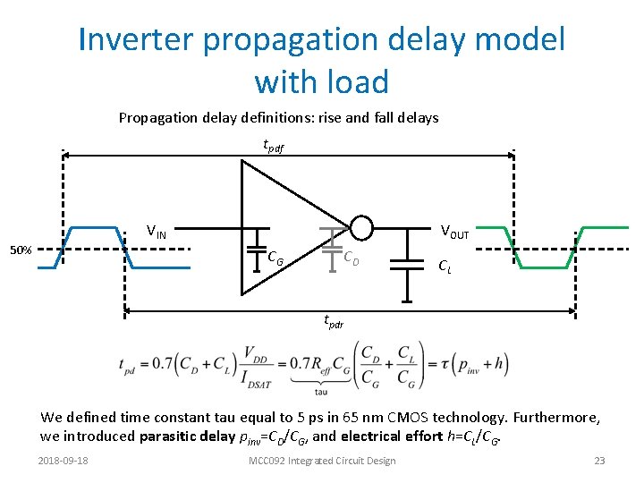
Delay with any load Equivalent electrical circuit for propagation delay calculations CL is the placeholder for the load capacitance. CL can be due to anything capacitive connected to the driving inverter’s output. VDD Reff CD CL If CL stems from inverters then CL is related to the widths of the loading inverters. Propagation delay: h = electrical effort 2018 -09 -13 Lecture 4: CMOS Inverter dynamics 18

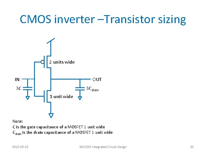
CMOS inverter –Transistor sizing 2 units wide IN OUT 3 C 3 Cdrain 1 unit wide Note: C is the gate capacitance of a MOSFET 1 unit wide Cdrain is the drain capacitance of a MOSFET 1 unit wide 2018 -09 -18 MCC 092 Integrated Circuit Design 20

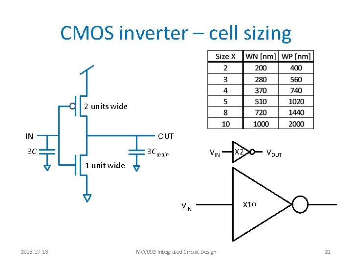
CMOS inverter – cell sizing 2 units wide IN OUT 3 C 3 Cdrain VIN X 2 VOUT 1 unit wide VIN 2018 -09 -18 MCC 092 Integrated Circuit Design X 10 21

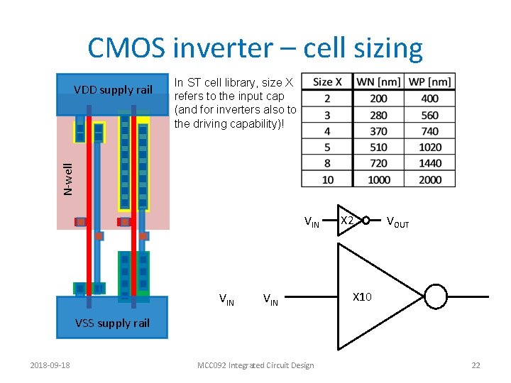
CMOS inverter – cell sizing In ST cell library, size X refers to the input cap (and for inverters also to the driving capability)! N-well VDD supply rail VIN VIN X 2 VOUT X 10 VSS supply rail 2018 -09 -18 MCC 092 Integrated Circuit Design 22

Inverter propagation delay model with load Propagation delay definitions: rise and fall delays tpdf VIN 50% VOUT CG CD CL tpdr We defined time constant tau equal to 5 ps in 65 nm CMOS technology. Furthermore, we introduced parasitic delay pinv=CD/CG, and electrical effort h=CL/CG. 2018 -09 -18 MCC 092 Integrated Circuit Design 23

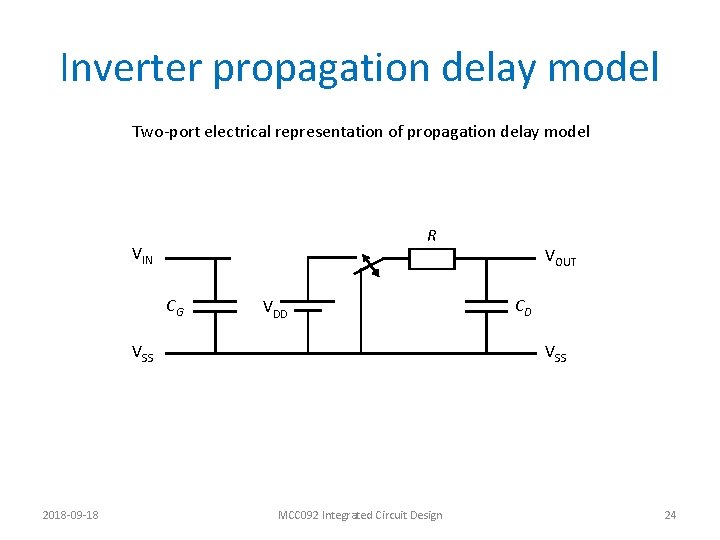
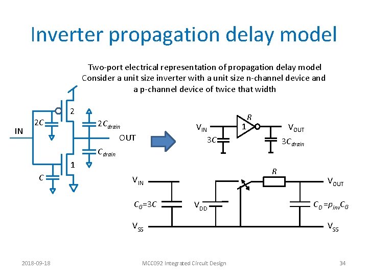
Inverter propagation delay model Two-port electrical representation of propagation delay model R VIN CG VDD VSS 2018 -09 -18 VOUT CD VSS MCC 092 Integrated Circuit Design 24

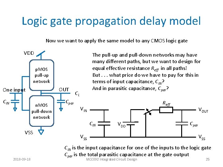
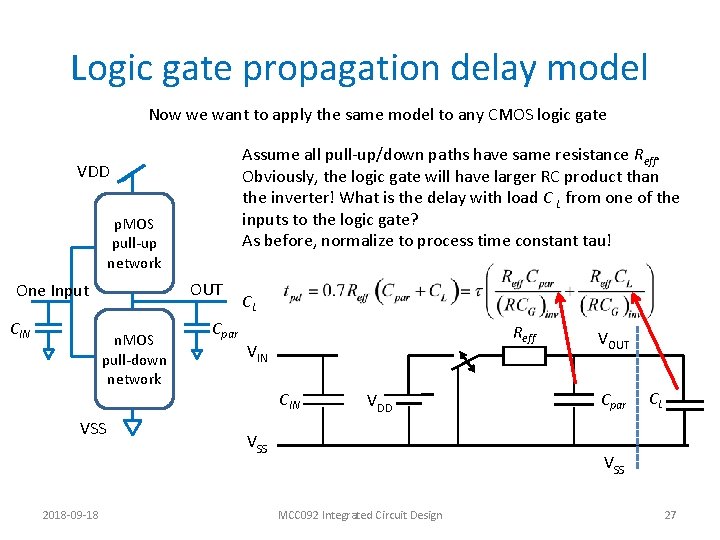
Logic gate propagation delay model Now we want to apply the same model to any CMOS logic gate VDD The pull-up and pull-down networks may have many different paths, but we want to design for equal effective resistance Reff in all paths! But. . . what price do we have to pay for this in terms of input capacitance, CIN? And in parasitic capacitance, Cpar? p. MOS pull-up network OUT One input CIN n. MOS pull-down network VSS 2018 -09 -18 Cpar CL Reff VIN CIN VDD VSS VOUT Cpar VSS CIN is the input capacitance for one of the inputs to the logic gate Cpar is the total parasitic capacitance at the gate output MCC 092 Integrated Circuit Design 25

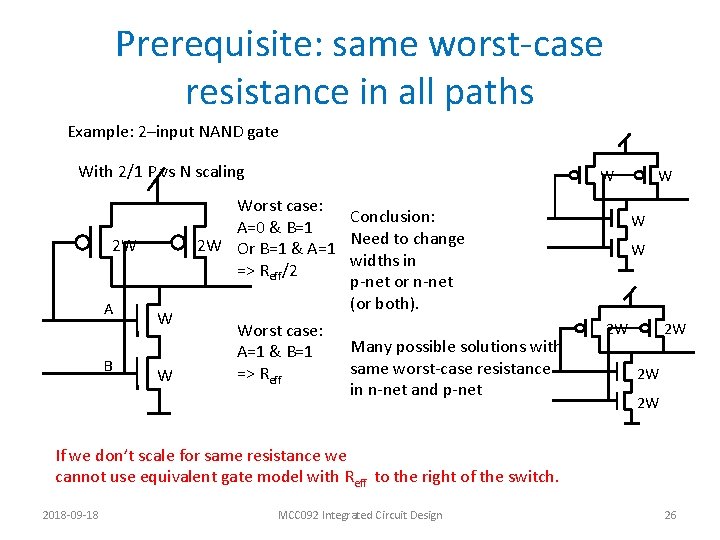
Prerequisite: same worst-case resistance in all paths Example: 2–input NAND gate With 2/1 P vs N scaling 2 W A B W Worst case: Conclusion: A=0 & B=1 2 W Or B=1 & A=1 Need to change widths in => Reff/2 p-net or n-net (or both). Worst case: Many possible solutions with A=1 & B=1 same worst-case resistance => Reff in n-net and p-net W W W 2 W 2 W If we don’t scale for same resistance we cannot use equivalent gate model with Reff to the right of the switch. 2018 -09 -18 MCC 092 Integrated Circuit Design 26

Logic gate propagation delay model Now we want to apply the same model to any CMOS logic gate Assume all pull-up/down paths have same resistance Reff. Obviously, the logic gate will have larger RC product than the inverter! What is the delay with load C L from one of the inputs to the logic gate? As before, normalize to process time constant tau! VDD p. MOS pull-up network OUT One Input CIN n. MOS pull-down network VSS 2018 -09 -18 Cpar CL Reff VIN CIN VDD VSS VOUT Cpar CL VSS MCC 092 Integrated Circuit Design 27

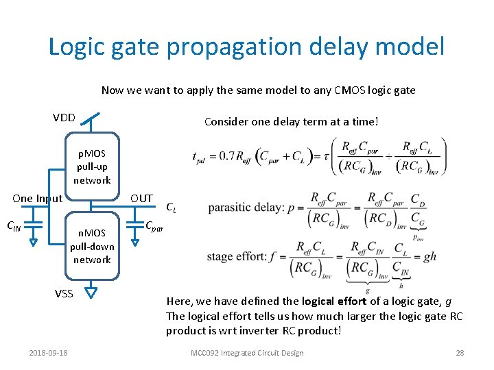
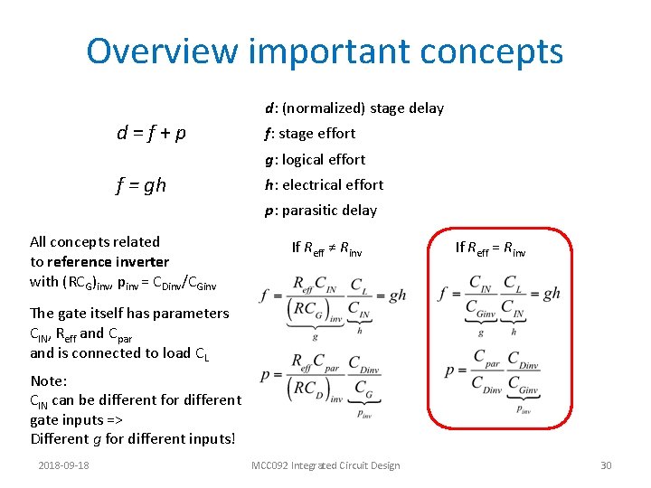
Logic gate propagation delay model Now we want to apply the same model to any CMOS logic gate VDD Consider one delay term at a time! p. MOS pull-up network One Input CIN OUT n. MOS pull-down network VSS 2018 -09 -18 CL Cpar Here, we have defined the logical effort of a logic gate, g The logical effort tells us how much larger the logic gate RC product is wrt inverter RC product! MCC 092 Integrated Circuit Design 28

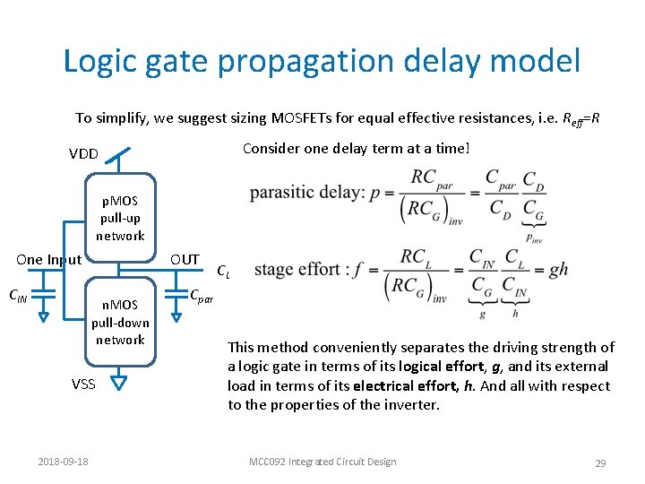
Logic gate propagation delay model To simplify, we suggest sizing MOSFETs for equal effective resistances, i. e. Reff=R Consider one delay term at a time! VDD p. MOS pull-up network One Input CIN OUT n. MOS pull-down network VSS 2018 -09 -18 CL Cpar This method conveniently separates the driving strength of a logic gate in terms of its logical effort, g, and its external load in terms of its electrical effort, h. And all with respect to the properties of the inverter. MCC 092 Integrated Circuit Design 29

Overview important concepts d: (normalized) stage delay d=f+p f: stage effort g: logical effort f = gh h: electrical effort p: parasitic delay All concepts related to reference inverter with (RCG)inv, pinv = CDinv/CGinv If Reff ≠ Rinv If Reff = Rinv The gate itself has parameters CIN, Reff and Cpar and is connected to load CL Note: CIN can be different for different gate inputs => Different g for different inputs! 2018 -09 -18 MCC 092 Integrated Circuit Design 30

Who invented logical effort? Ivan Sutherland Bob Sproull “The father of computer graphics” Together they worked on head-mounted displays. Work on graphics hardware spurred the invention of logical effort 2018 -09 -18 MCC 092 Integrated Circuit Design 31

Quiz time! Go to socrative. com Select Student login Go to room: “MCC 0922018” 2018 -09 -18 MCC 092 Integrated Circuit Design 32

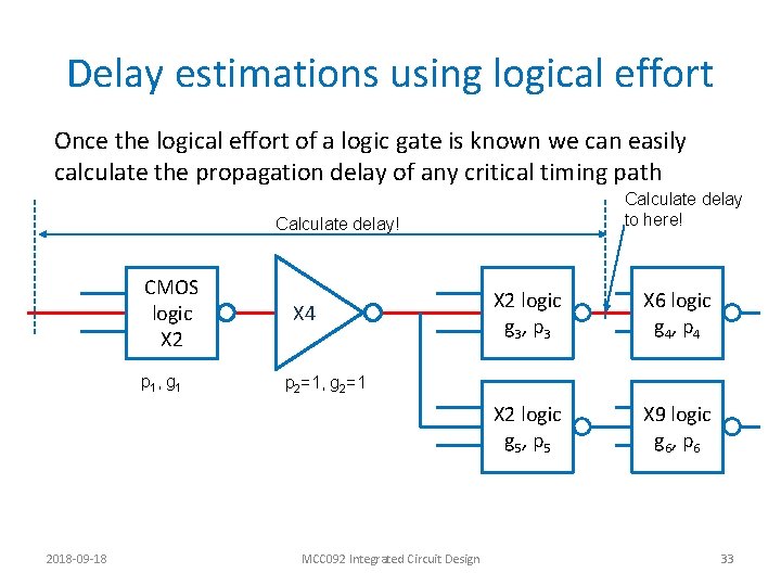
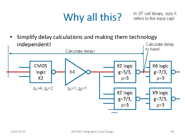
Delay estimations using logical effort Once the logical effort of a logic gate is known we can easily calculate the propagation delay of any critical timing path Calculate delay to here! Calculate delay! CMOS logic X 2 p 1 , g 1 2018 -09 -18 X 4 X 2 logic g 3 , p 3 X 6 logic g 4 , p 4 X 2 logic g 5 , p 5 X 9 logic g 6 , p 6 p 2=1, g 2=1 MCC 092 Integrated Circuit Design 33

Inverter propagation delay model Two-port electrical representation of propagation delay model Consider a unit size inverter with a unit size n-channel device and a p-channel device of twice that width 2 IN 2 C 2 Cdrain 1 VIN OUT R VOUT 3 C 3 Cdrain 1 C R VIN CG=3 C VDD VSS 2018 -09 -18 MCC 092 Integrated Circuit Design VOUT CD =pinv. CG VSS 34

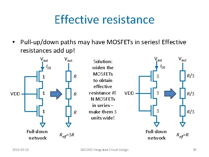
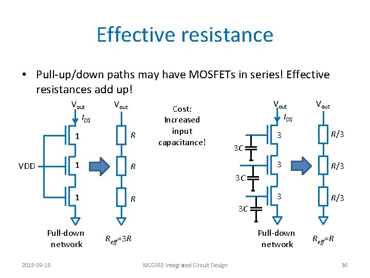
Effective resistance • Pull-up/down paths may have MOSFETs in series! Effective resistances add up! Vout IDS VDD 1 R 1 R Pull-down network 2018 -09 -18 Vout Solution: widen the MOSFETs to obtain effective resistance R! N MOSFETs in series – make them 3 units wide! Vout IDS VDD 3 R/3 Pull-down network Reff=3 R MCC 092 Integrated Circuit Design Vout Reff=R 35

Effective resistance • Pull-up/down paths may have MOSFETs in series! Effective resistances add up! Vout IDS 1 1 VDD 1 Pull-down network 2018 -09 -18 Vout R Cost: Increased input capacitance! R Vout IDS Vout 3 R/3 3 C 3 C R 3 C Pull-down network Reff=3 R MCC 092 Integrated Circuit Design Reff=R 36

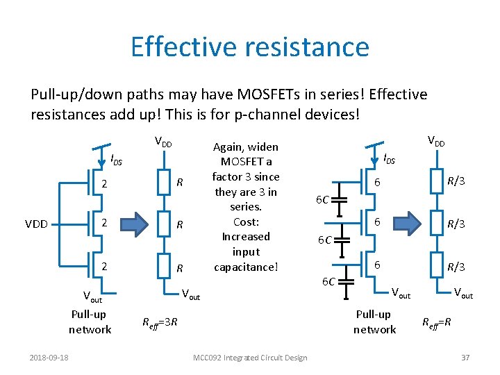
Effective resistance Pull-up/down paths may have MOSFETs in series! Effective resistances add up! This is for p-channel devices! VDD Again, widen MOSFET a factor 3 since they are 3 in series. Cost: Increased input capacitance! IDS 2 VDD 2 2 Vout Pull-up network 2018 -09 -18 R R R Vout VDD IDS 6 R/3 6 C 6 C 6 C Vout Pull-up network Reff=3 R MCC 092 Integrated Circuit Design Vout Reff=R 37

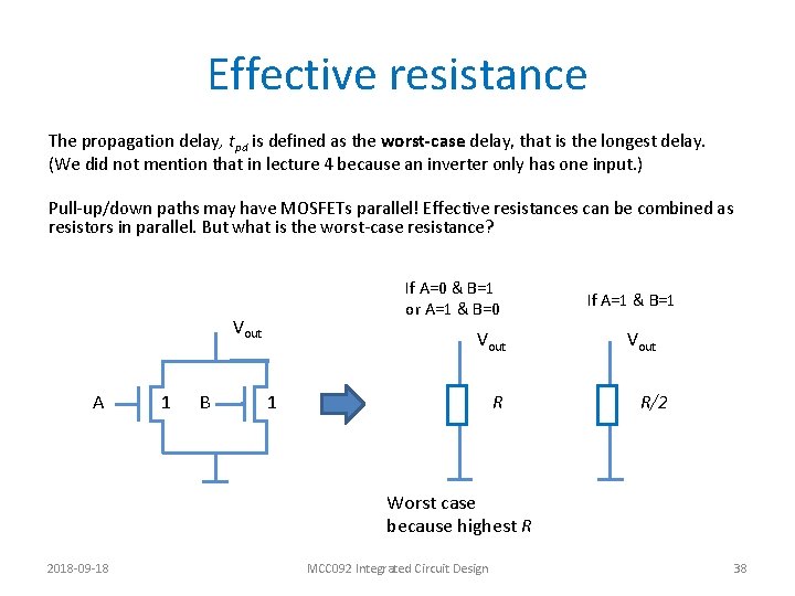
Effective resistance The propagation delay, tpd is defined as the worst-case delay, that is the longest delay. (We did not mention that in lecture 4 because an inverter only has one input. ) Pull-up/down paths may have MOSFETs parallel! Effective resistances can be combined as resistors in parallel. But what is the worst-case resistance? If A=0 & B=1 or A=1 & B=0 Vout A 1 B Vout 1 R If A=1 & B=1 Vout R/2 Worst case because highest R 2018 -09 -18 MCC 092 Integrated Circuit Design 38

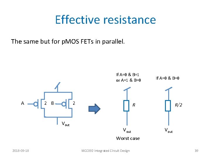
Effective resistance The same but for p. MOS FETs in parallel. If A=0 & B=1 or A=1 & B=0 A 2 B 2 Vout If A=0 & B=0 R Vout R/2 Vout Worst case 2018 -09 -18 MCC 092 Integrated Circuit Design 39

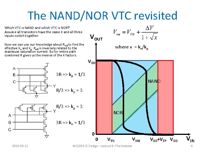
The NAND/NOR VTC revisited Which VTC is NAND and which VTC is NOR? Assume all transistors have the same k and all three inputs switch together. VOUT Now we can use our knowledge about R eff to find the effective kn and kp. Reff is inversely related to the maximum saturation current. So for entire path combined R gives us the inverse of the k factors. where x = kn/kp VDD 3 R => kp = 1/3 NAND R/3 => kn = 3 R/3 => kp = 3 NOR 3 R => kn = 1/3 0 2018 -09 -11 0 VTN MCC 092 IC Design - Lecture 3: The Inverter VSW VDD+VTP VDD VIN 8

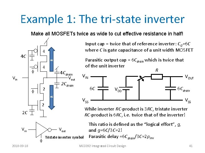
Example 1: The tri-state inverter Make all MOSFETs twice as wide to cut effective resistance in half! Input cap = twice that of reference inverter: CG=6 C where C is gate capacitance of a unit width MOSFET 4 Parasitic output cap = 6 Cdrain which is twice that of the unit inverter R R 4 C _ f 4 4 Cdrain Vout 2 Cdrain 2 R f VIN 6 C VDD 6 Cdrain VSS 2 VOUT VSS 2 C While inverter RC-product is 3 RC, tristate inverter RC-product is 6 RC, i. e. twice that of the inverter! Vin This ratio is defined as the “logical effort”, g, and g=6 C/3 C=2! Parasitic delay =6 Cdrain/3 C=2 pinv Vout f 2018 -09 -18 Tristate inverter symbol MCC 092 Integrated Circuit Design 41

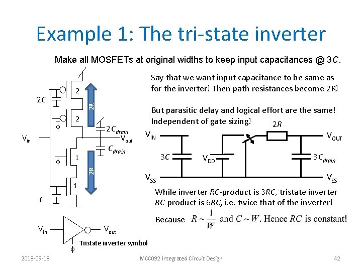
Example 1: The tri-state inverter Make all MOSFETs at original widths to keep input capacitances @ 3 C. Say that we want input capacitance to be same as for the inverter! Then path resistances become 2 R! 2 2 R 2 C _ f 2 2 Cdrain Vout VIN Cdrain 1 2 R f But parasitic delay and logical effort are the same! Independent of gate sizing! 2 R 3 C 2018 -09 -18 3 Cdrain VSS While inverter RC-product is 3 RC, tristate inverter RC-product is 6 RC, i. e. twice that of the inverter! C Because Vout f VDD VSS 1 Vin VOUT Tristate inverter symbol MCC 092 Integrated Circuit Design 42

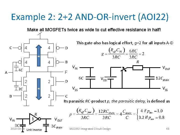
Example 2: 2+2 AND-OR-invert (AOI 22) Make all MOSFETs twice as wide to cut effective resistance in half! This gate also has logical effort, g=2 for all inputs A-D 4 A 4 4 D 4 B R C 4 C A A F 2 B 2 1 VIN 3 C 2018 -09 -18 Unit inverter VDD VOUT 12 Cdrain VSS C 2 R 6 C VSS R 2 C VIN D 2 R Its parasitic RC-product p, the parasitic delay, is defined as VOUT 3 Cdrain MCC 092 Integrated Circuit Design 43

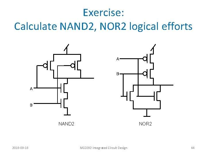
Exercise: Calculate NAND 2, NOR 2 logical efforts A B NAND 2 2018 -09 -18 NOR 2 MCC 092 Integrated Circuit Design 44

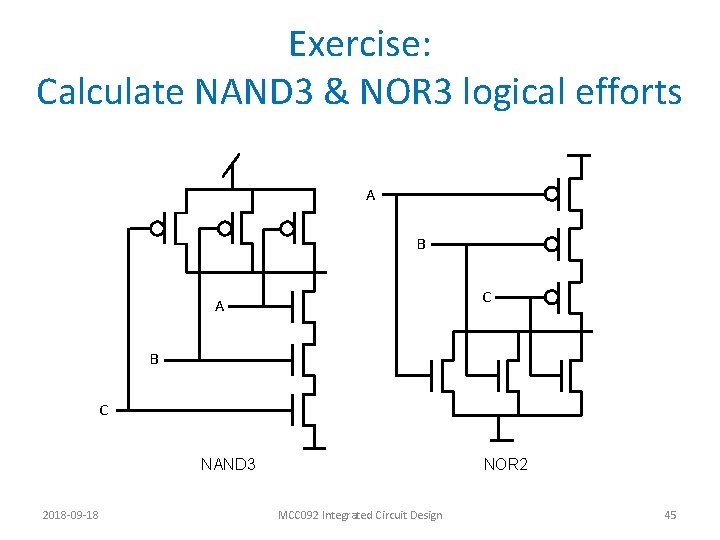
Exercise: Calculate NAND 3 & NOR 3 logical efforts A B C NAND 3 2018 -09 -18 NOR 2 MCC 092 Integrated Circuit Design 45

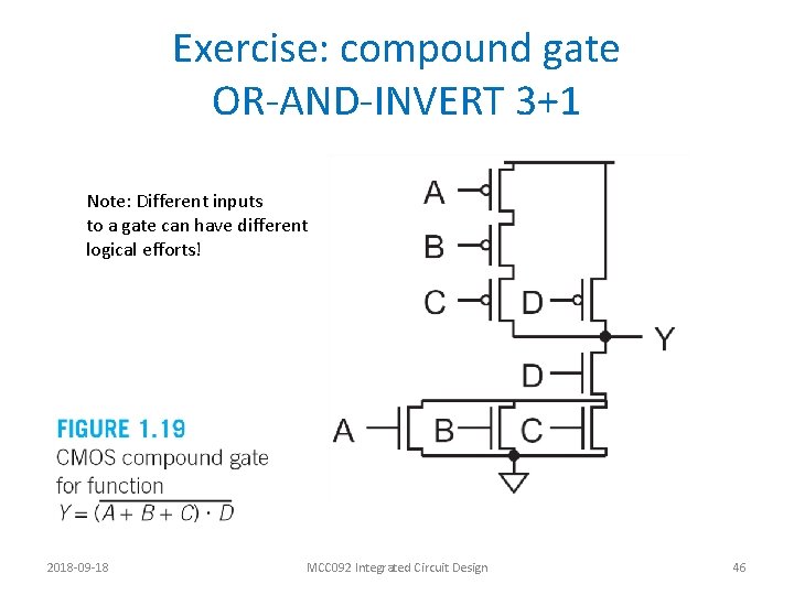
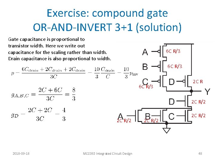
Exercise: compound gate OR-AND-INVERT 3+1 Note: Different inputs to a gate can have different logical efforts! 2018 -09 -18 MCC 092 Integrated Circuit Design 46

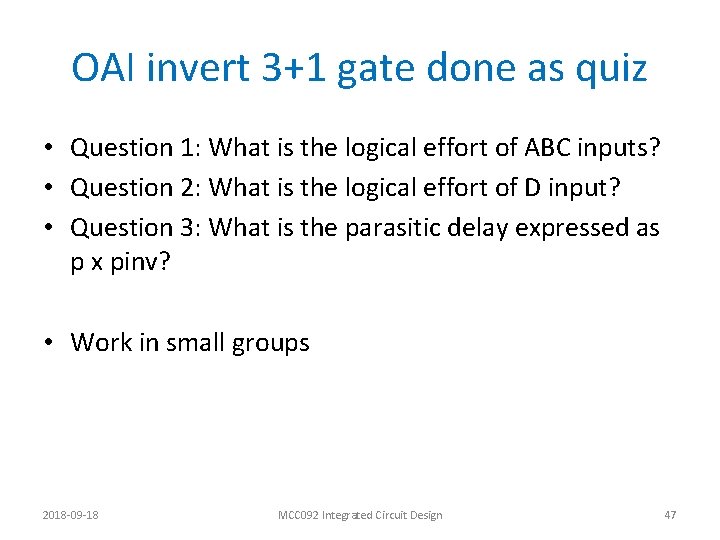
OAI invert 3+1 gate done as quiz • Question 1: What is the logical effort of ABC inputs? • Question 2: What is the logical effort of D input? • Question 3: What is the parasitic delay expressed as p x pinv? • Work in small groups 2018 -09 -18 MCC 092 Integrated Circuit Design 47

Exercise: compound gate OR-AND-INVERT 3+1 (solution) Gate capacitance is proportional to transistor width. Here we write out capacitance for the scaling rather than width. Drain capacitance is also proportional to width. 6 C R/3 2 C R/2 2018 -09 -18 MCC 092 Integrated Circuit Design 2 C R/2 48

Why all this? In ST cell library, size X refers to the input cap! • Simplify delay calculations and making them technology Calculate delay independent! to here! Calculate delay! CMOS logic X 2 p 1=4, g 1=2 X 4 p 2=1, g 2=1 X 2 logic g=5/3, p=3 X 6 logic g=7/3, p=3 X 2 logic g=7/3, p=3 X 9 logic g=7/3, p=3 Propagation delay=18*tao=90 ps 2018 -09 -18 MCC 092 Integrated Circuit Design 49

Why all this? • Minimize path delays with gates other than inverters. • We will do that in lecture 6. 2018 -09 -18 MCC 092 Integrated Circuit Design 50

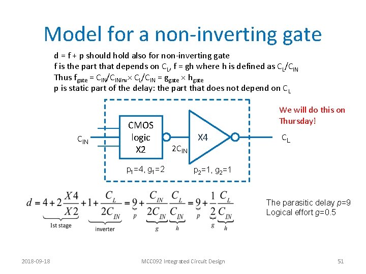
Model for a non-inverting gate d = f + p should hold also for non-inverting gate f is the part that depends on CL, f = gh where h is defined as CL/CIN Thus fgate = CIN/CINinv× CL/CIN = ggate × hgate p is static part of the delay: the part that does not depend on CL CIN CMOS logic X 2 p 1=4, g 1=2 We will do this on Thursday! 2 CIN X 4 CL p 2=1, g 2=1 The parasitic delay p=9 Logical effort g=0. 5 2018 -09 -18 MCC 092 Integrated Circuit Design 51

Overview important concepts d: (normalized) stage delay d=f+p f: stage effort g: logical effort f = gh h: electrical effort p: parasitic delay All concepts related to reference inverter with (RCG)inv, pinv = CDinv/CGinv If Reff ≠ Rinv If Reff = Rinv The gate itself has parameters CIN, Reff and Cpar and is connected to load CL Note: CIN can be different for different gate inputs => Different g for different inputs! 2018 -09 -18 MCC 092 Integrated Circuit Design 52

Conclusion In this lecture we have • Adapted the two-port delay model previously developed for inverters to any CMOS logic gate • Learnt how to size MOSFETs for equal worst case rise and fall delay • Noticed that logic gates have larger Reff. CG products than inverters • Introduced two new concepts: logical effort and parasitic delay • Logical effort and parasitic delay quantifies – Logical effort: (Reff. CG)gate relative to (3 RC)inv – Parasitic delay: (Reff. Cpar)gate relative to (3 RC)inv • Learnt how to calculate these parameters for any logic gate • Learnt how to calculate the electrical effort h= CLOAD/CIN • Learnt to calculate all propagation delays as a multiple of tau, where tau=5 ps in STMicroelectronics 65 nm CMOS process 2018 -09 -18 MCC 092 Integrated Circuit Design 53