CMOS Layout Design Rules Dr Zakir Ali Asstt

- Slides: 26

CMOS Layout Design Rules Dr. Zakir Ali, Asstt. Prof. Deptt. OF ECE. Email : zakirali 008@gmail. com 6/3/2021 Layout-design Lect-9

CMOS DESIGN RULES • Fabrication processes are pattern independent. • Design Rules are constraints poses by processing line in the form of minimum allowable values for width, separation, extension and overlap. • The complexity of design rules depends upon how well a process is characterized. 6/3/2021 Layout-design Lect-9

CMOS DESIGN RULES (con. ) A proper set of design rules must take into account the following considerations: • Characteristic of Photolithography. • Etching capabilities. • Expected misalignment Variance. • Electrical Constraints. 6/3/2021 Layout-design Lect-9

Photolithography Constraints: • Minimum geometry to be resolved in the photoresist. • Impose condition on minimum line width and separation. • Width and spacing rules must be relaxed to the upper most non-uniform layer. 6/3/2021 Layout-design Lect-9

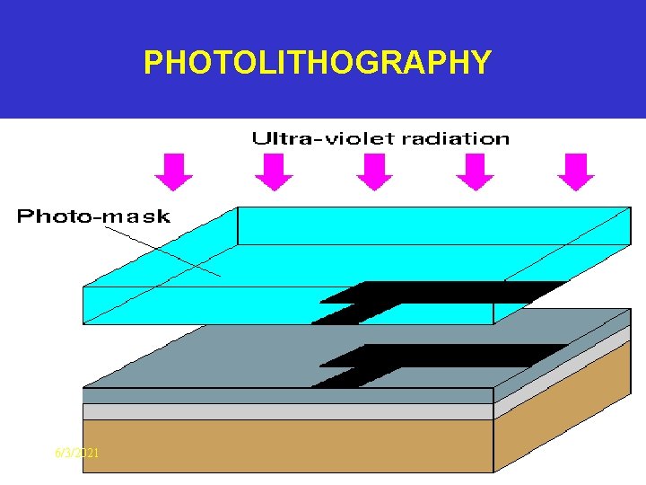
PHOTOLITHOGRAPHY 6/3/2021 Layout-design Lect-9

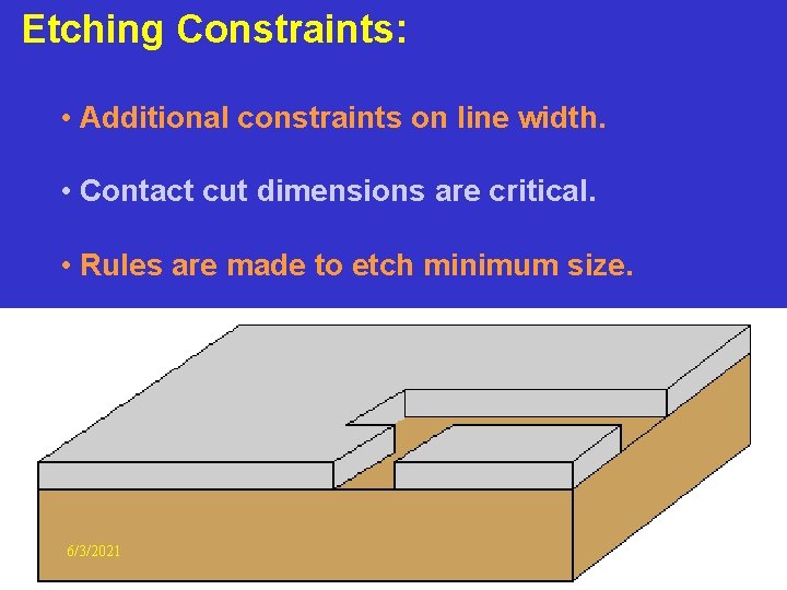
Etching Constraints: • Additional constraints on line width. • Contact cut dimensions are critical. • Rules are made to etch minimum size. 6/3/2021 Layout-design Lect-9

Misalignment Variance: • All subsequent layers are aligned with previous layer • Proper choice of alignment sequence plays important role. Electrical Constraints: • No physical contact in adjacent lines. • Minimum line width must be wide enough to avoid electromigration. 6/3/2021 Layout-design Lect-9

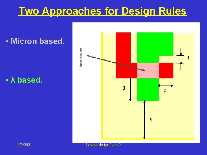
Two Approaches for Design Rules • Micron based. • λ based. 6/3/2021 Layout-design Lect-9

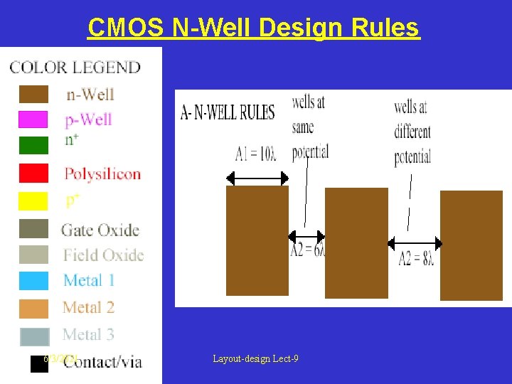
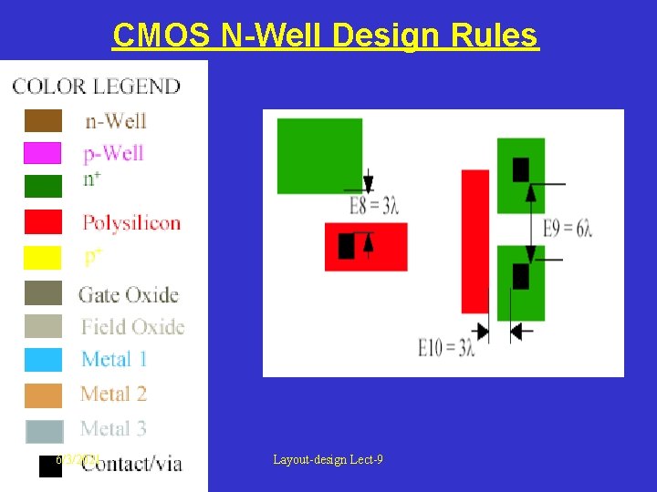
CMOS N-Well Design Rules 6/3/2021 Layout-design Lect-9

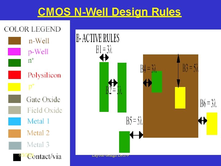
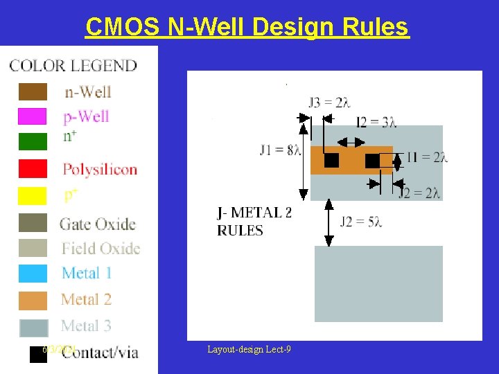
CMOS N-Well Design Rules 6/3/2021 Layout-design Lect-9

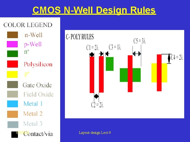
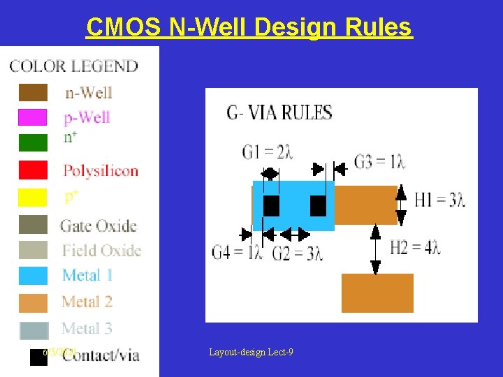
CMOS N-Well Design Rules 6/3/2021 Layout-design Lect-9

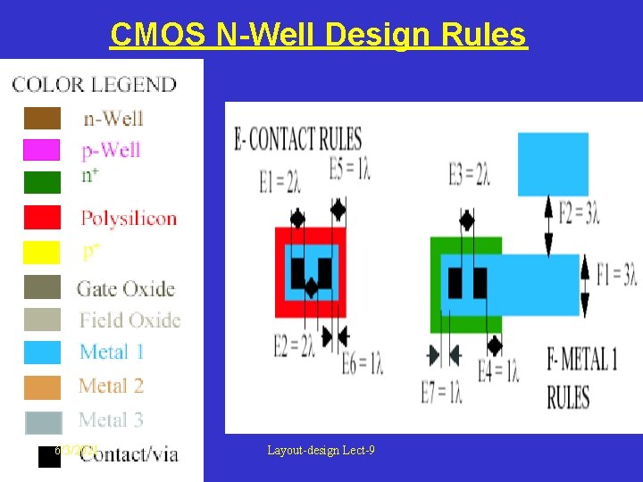
CMOS N-Well Design Rules 6/3/2021 Layout-design Lect-9

CMOS N-Well Design Rules 6/3/2021 Layout-design Lect-9

CMOS N-Well Design Rules 6/3/2021 Layout-design Lect-9

CMOS N-Well Design Rules 6/3/2021 Layout-design Lect-9

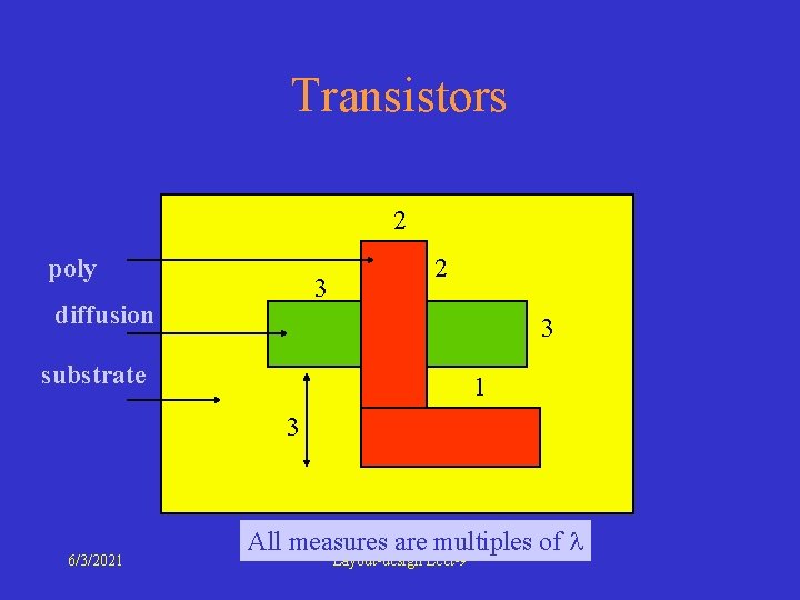
Transistors 2 poly 3 diffusion 2 3 substrate 1 3 6/3/2021 All measures are multiples of Layout-design Lect-9

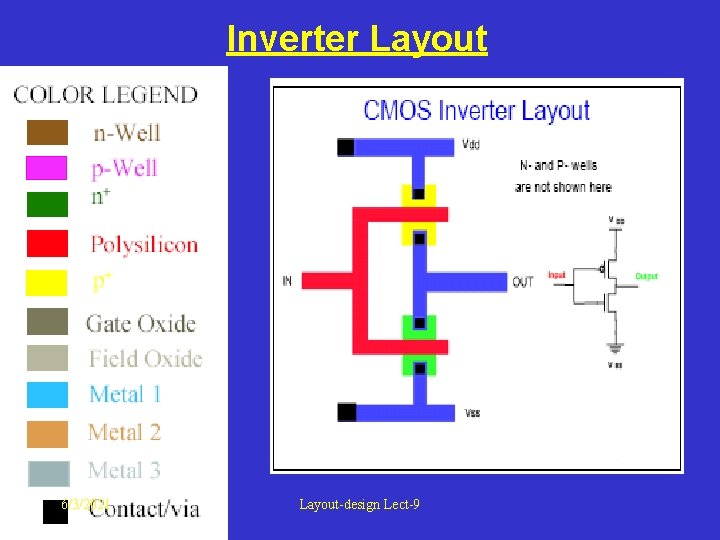
Inverter Layout 6/3/2021 Layout-design Lect-9

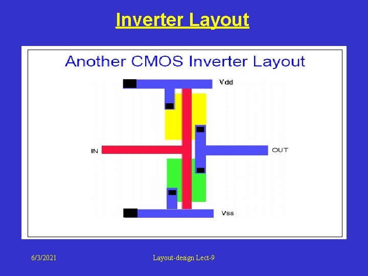
Inverter Layout 6/3/2021 Layout-design Lect-9

6/3/2021 Layout-design Lect-9

6/3/2021 Layout-design Lect-9

6/3/2021 Layout-design Lect-9

6/3/2021 Layout-design Lect-9

6/3/2021 Layout-design Lect-9

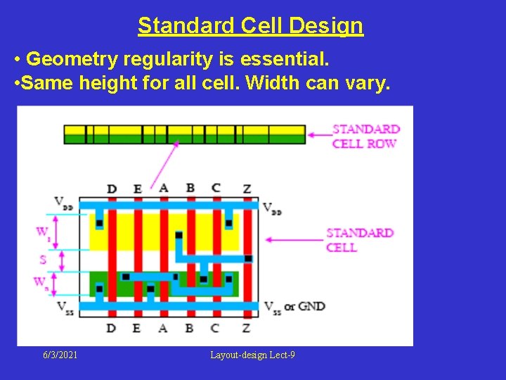
Standard Cell Design • Geometry regularity is essential. • Same height for all cell. Width can vary. 6/3/2021 Layout-design Lect-9

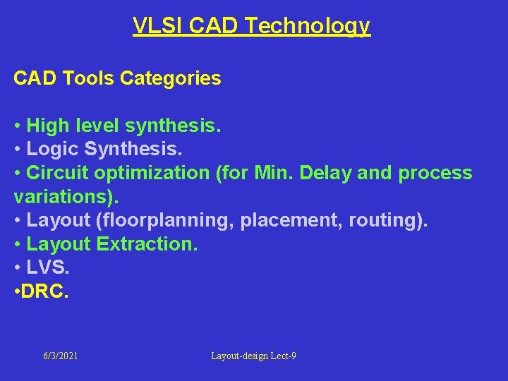
VLSI CAD Technology CAD Tools Categories • High level synthesis. • Logic Synthesis. • Circuit optimization (for Min. Delay and process variations). • Layout (floorplanning, placement, routing). • Layout Extraction. • LVS. • DRC. 6/3/2021 Layout-design Lect-9

Next Class Topic Design of NAND, NOR and AOI Gates 6/3/2021 Layout-design Lect-9