CMOS Inverter CMOS Inverter Switch Model of Dynamic
- Slides: 12

CMOS Inverter

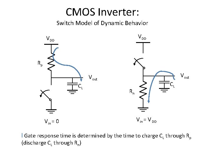
CMOS Inverter: Switch Model of Dynamic Behavior VDD Rp Vout CL Vin = 0 CL Rn Vin = V DD l Gate response time is determined by the time to charge CL through Rp (discharge CL through Rn)

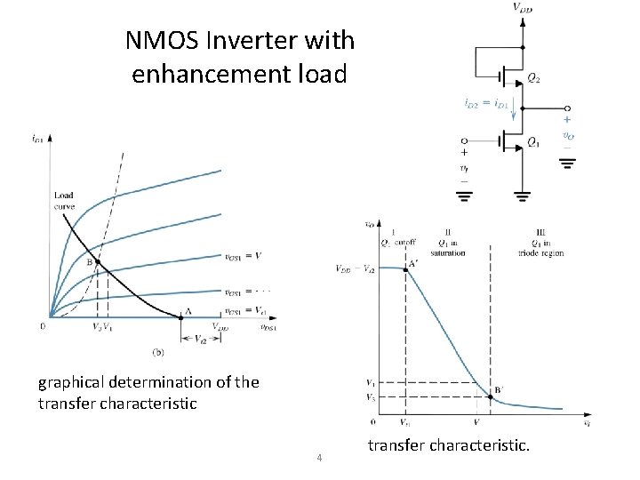
NMOS Inverter with enhancement load graphical determination of the transfer characteristic 4 transfer characteristic.

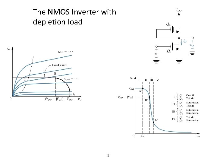
The NMOS Inverter with depletion load 5

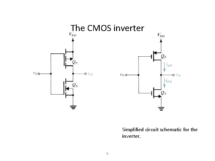
The CMOS inverter Simplified circuit schematic for the inverter. 6

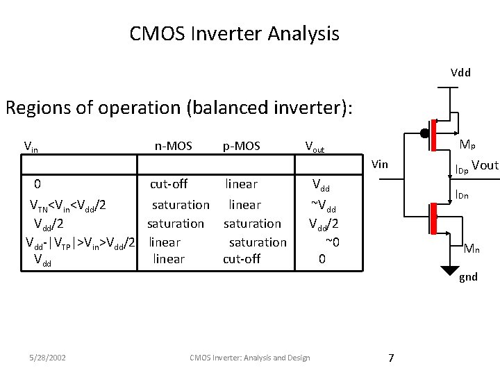
CMOS Inverter Analysis Vdd Regions of operation (balanced inverter): Vin n-MOS p-MOS Mp IDp Vout Vin 0 cut-off linear VTN<Vin<Vdd/2 saturation linear Vdd/2 saturation Vdd-|VTP|>Vin>Vdd/2 linear saturation Vdd linear cut-off Vdd ~Vdd Vdd/2 ~0 0 IDn Mn gnd 5/28/2002 CMOS Inverter: Analysis and Design 7

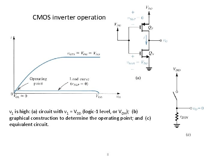
CMOS inverter operation v 1 is high: (a) circuit with v 1 = VDD (logic-1 level, or VOH); (b) graphical construction to determine the operating point; and (c) equivalent circuit. 8

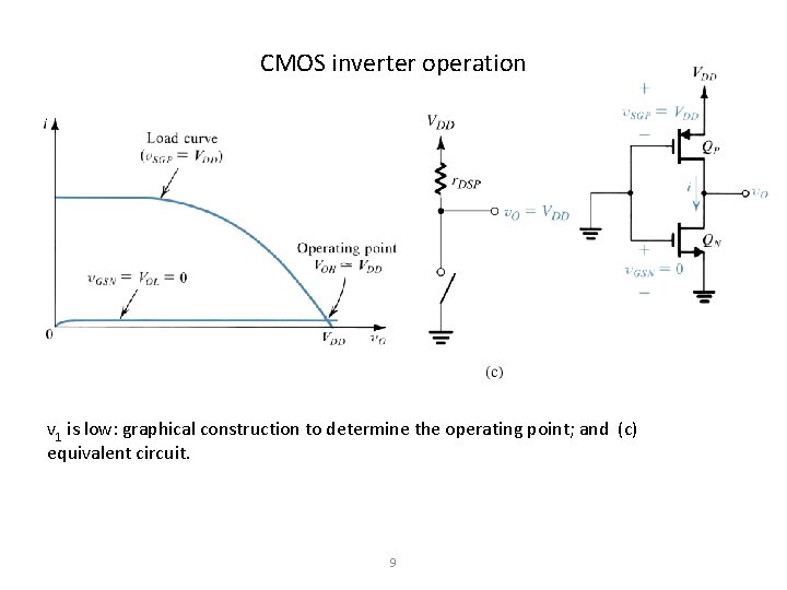
CMOS inverter operation v 1 is low: graphical construction to determine the operating point; and (c) equivalent circuit. 9

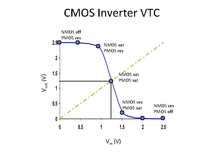
CMOS Inverter VTC NMOS off PMOS res Vout (V) NMOS sat PMOS res NMOS sat PMOS sat NMOS res PMOS sat Vin (V) NMOS res PMOS off

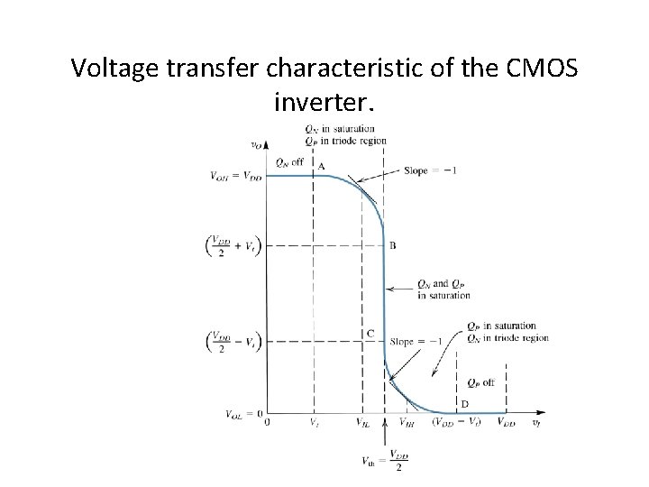
Voltage transfer characteristic of the CMOS inverter. 12

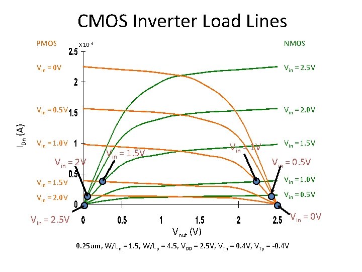
CMOS Inverter Load Lines IDn (A) PMOS NMOS X 10 -4 Vin = 0 V Vin = 2. 5 V Vin = 0. 5 V Vin = 2. 0 V Vin = 1. 0 V Vin = 2 V Vin = 1. 5 V Vin = 0. 5 V Vin = 1. 0 V Vin = 2. 0 V Vin = 0. 5 V Vin = 2. 5 V Vin = 0 V Vout (V) 0. 25 um, W/Ln = 1. 5, W/Lp = 4. 5, VDD = 2. 5 V, VTn = 0. 4 V, VTp = -0. 4 V

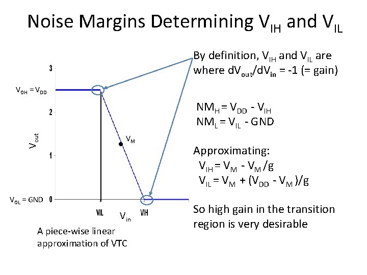
Noise Margins Determining VIH and VIL By definition, VIH and VIL are where d. Vout/d. Vin = -1 (= gain) VOH = VDD Vout NMH = VDD - VIH NML = VIL - GND VM VOL = GND Vin A piece-wise linear approximation of VTC Approximating: VIH = VM - VM /g VIL = VM + (VDD - VM )/g So high gain in the transition region is very desirable