CMOS Image Sensor developments supported by the European
CMOS Image Sensor developments supported by the European Space Agency Kyriaki Minoglou European Space Agency ESTEC P. O. Box 299, 2200 AG Noordwijk The Netherlands 2018 EIROForum Topical Workshop: CMOS Sensors CERN, Switzerland 25 June 2018
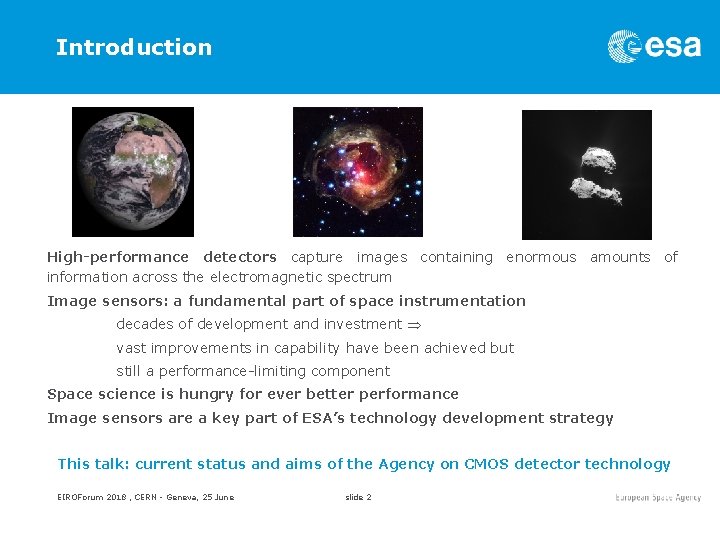
Introduction High-performance detectors capture images containing enormous amounts of information across the electromagnetic spectrum Image sensors: a fundamental part of space instrumentation decades of development and investment vast improvements in capability have been achieved but still a performance-limiting component Space science is hungry for ever better performance Image sensors are a key part of ESA’s technology development strategy This talk: current status and aims of the Agency on CMOS detector technology EIROForum 2018 , CERN - Geneva, 25 June slide 2
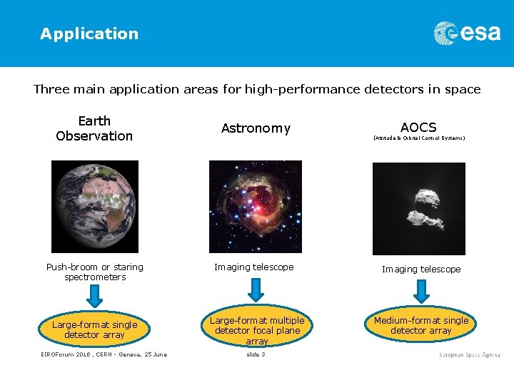
Application Three main application areas for high-performance detectors in space Earth Observation Push-broom or staring spectrometers Large-format single detector array EIROForum 2018 , CERN - Geneva, 25 June Astronomy Imaging telescope Large-format multiple detector focal plane array slide 3 AOCS (Attitude & Orbital Control Systems) Imaging telescope Medium-format single detector array
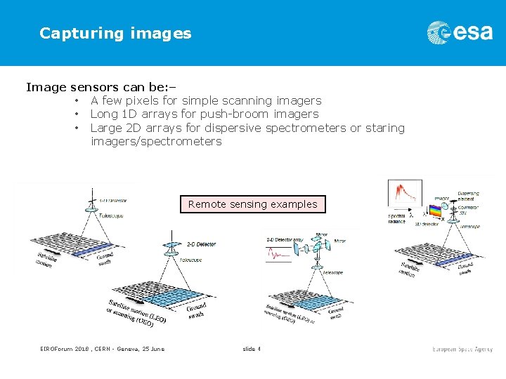
Capturing images Image sensors can be: – • A few pixels for simple scanning imagers • Long 1 D arrays for push-broom imagers • Large 2 D arrays for dispersive spectrometers or staring imagers/spectrometers Remote sensing examples EIROForum 2018 , CERN - Geneva, 25 June slide 4
Detector requirements Detectors are a performance limiting component for space instrumentation a) Instrument requirements – tend to be determined by the state-ofthe-art + ‘better than before’ b) Functionality and performance of optical instruments – determined by available detectors Usually not the same thing -> continuous detector development and improvement EIROForum 2018 , CERN - Geneva, 25 June slide 5
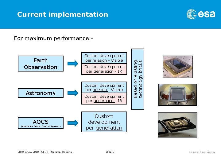
Current implementation Earth Observation Astronomy AOCS (Attitude & Orbital Control Systems) EIROForum 2018 , CERN - Geneva, 25 June Custom development per mission - Visible Custom development per generation - IR Custom development per generation slide 6 Based on existing technology bricks For maximum performance -
Space detector requirements Requirements for high-performance detectors in space are not always the same as those for commercial applications Generalising On-ground Lots & lots of small pixels, colour output, TV formats (HD, UHD…) or Film formats (APS-C, 35 mm) video frame rates, digital output, … In-space Lots of large pixels, monochrome output, custom formats, variable frame rates (m. Hz 10’s Hz), analogue output, … and reliability! Still some common goals high QE, low dark current, good imaging performance (MTF, PRNU), high dynamic range, … … and good overlap with ground-based science & astronomy. EIROForum 2018 , CERN - Geneva, 25 June slide 7
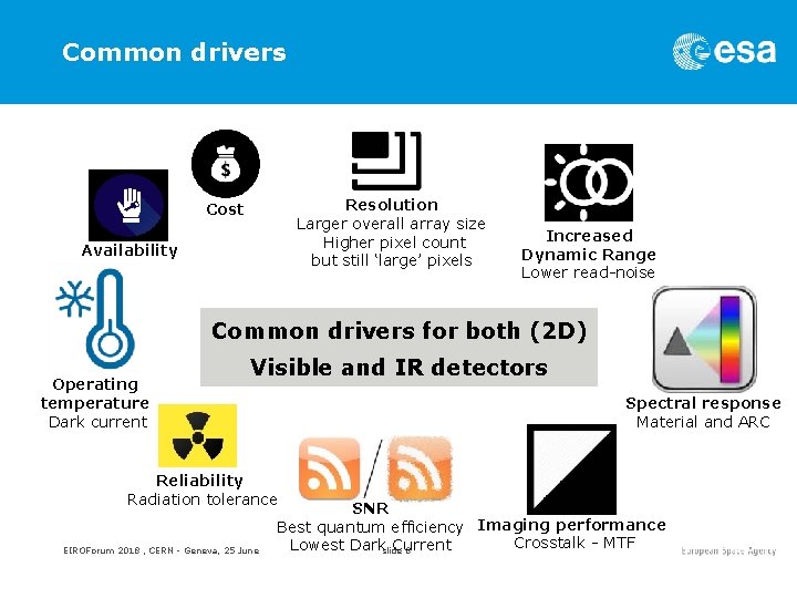
Common drivers Resolution Larger overall array size Higher pixel count but still ‘large’ pixels Cost Availability Increased Dynamic Range Lower read-noise Common drivers for both (2 D) Operating temperature Dark current Visible and IR detectors Spectral response Material and ARC Reliability Radiation tolerance EIROForum 2018 , CERN - Geneva, 25 June SNR Best quantum efficiency Imaging performance Crosstalk - MTF Lowest Dark Current slide 8
Materials Effectively two ‘workhorse’ materials for high-performance imaging sensors in space – • UV-Visible waveband– Silicon Ubiquitous material for commercial ICs and detectors (mobile phones, digital cameras etc). Response from UV to 1. 1 um. Available in large wafer sizes, very high quality and with custom parameters (e. g. epi thickness, resistivity). Array detector types – monolithic CCD or CIS, hybrid CIS • NIR/SWIR Infrared waveband – Mercury Cadmium Telluride (MCT or Hg. Cd. Te) Tertiary material semiconductor alloy with adjustable cut-off wavelength – from <2 um to 20 um+. Array detector types – hybrid CIS EIROForum 2018 , CERN - Geneva, 25 June But - willing to work with other materials slide 9 to get best performance
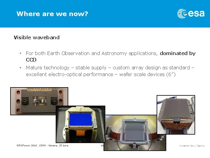
Where are we now? Visible waveband • For both Earth Observation and Astronomy applications, dominated by CCD • Mature technology – stable supply – custom array design as standard – excellent electro-optical performance – wafer scale devices (6”) EIROForum 2018 , CERN - Geneva, 25 June slide 10
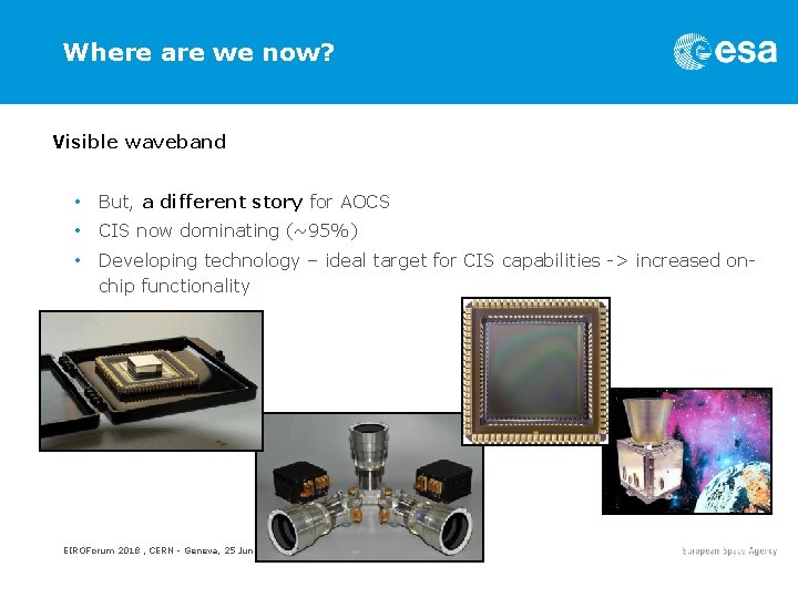
Where are we now? Visible waveband • But, a different story for AOCS • CIS now dominating (~95%) • Developing technology – ideal target for CIS capabilities -> increased onchip functionality EIROForum 2018 , CERN - Geneva, 25 June slide 11
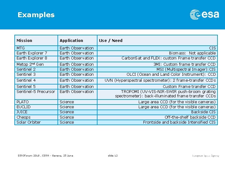
Examples Mission Application MTG Earth Explorer 7 Earth Explorer 8 Earth Observation CIS Biomass: Not applicable Carbon. Sat and FLEX: custom Frame transfer CCD Metop 2 nd Gen Sentinel 2 Sentinel 3 Earth Observation 3 MI: Custom frame transfer CCD MSI (Multispectral Imager): CIS OLCI (Ocean and Land Color Instrument): CCD Sentinel 4 Earth Observation UVN (Hyperspectral spectrometer): 2 frame-transfer CCDs Sentinel 5 Sentinel-5 Precursor Earth Observation Custom Frame transfer CCD TROPOMI (UV-VIS-NIR-SWIR push-broom grating spectrometer): back-illuminated frame transfer CCDs PLATO EUCLID JUICE Cheops Solar Orbiter Science Science EIROForum 2018 , CERN - Geneva, 25 June Use / Need Large area CCD (for the visible cameras) Backside CIS Off-the-shelf backside CCD Frontside and backside Intensified CIS slide 12
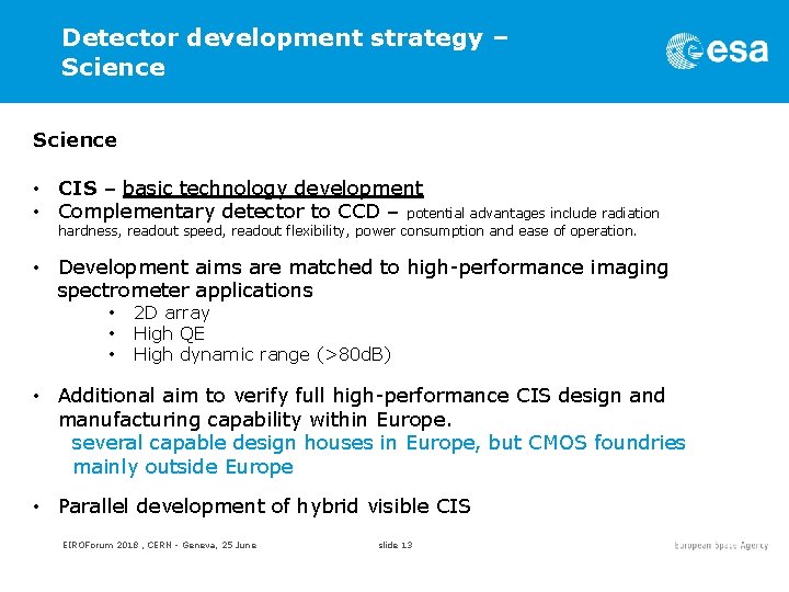
Detector development strategy – Science • CIS – basic technology development • Complementary detector to CCD – potential advantages include radiation hardness, readout speed, readout flexibility, power consumption and ease of operation. • Development aims are matched to high-performance imaging spectrometer applications • • • 2 D array High QE High dynamic range (>80 d. B) • Additional aim to verify full high-performance CIS design and manufacturing capability within Europe. several capable design houses in Europe, but CMOS foundries mainly outside Europe • Parallel development of hybrid visible CIS EIROForum 2018 , CERN - Geneva, 25 June slide 13
CMOS in Europe: Development Options 1. European design house coupled with non-European foundry likely to provide the best performance in the shorter term, but is only partial non-dependence and consequently subject to more external influences. 2. European design house coupled to European foundry implies full European non-dependence and potentially better control over the processes. Unfortunately, the current situation for CIS manufacturing capabilities is not in line with the demand expectation of industry. Industry is strongly suffering from this situation, despite the following actions that tried to alleviate the situation: • actions launched by ESA during the 2 last years (Euro. CIS High flux and Low flux) See next slide • FP 7 funding (IMEC action) • actions and funding from national agencies for space dedicated CIS (CNES and DLR) • actions supported by other national funding (French PIA, UK actions) EIROForum 2018 , CERN - Geneva, 25 June slide 14
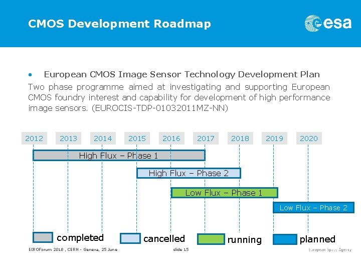
CMOS Development Roadmap • European CMOS Image Sensor Technology Development Plan Two phase programme aimed at investigating and supporting European CMOS foundry interest and capability for development of high performance image sensors. (EUROCIS-TDP-01032011 MZ-NN) 2012 2013 2014 2015 2016 2017 2018 2019 2020 High Flux – Phase 1 High Flux – Phase 2 Low Flux – Phase 1 Low Flux – Phase 2 completed EIROForum 2018 , CERN - Geneva, 25 June cancelled slide 15 running planned
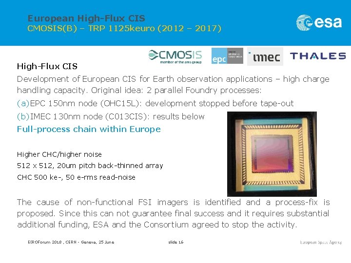
European High-Flux CIS CMOSIS(B) – TRP 1125 keuro (2012 – 2017) High-Flux CIS Development of European CIS for Earth observation applications – high charge handling capacity. Original idea: 2 parallel Foundry processes: (a) EPC 150 nm node (OHC 15 L): development stopped before tape-out (b) IMEC 130 nm node (C 013 CIS): results below Full-process chain within Europe Higher CHC/higher noise 512 x 512, 20 um pitch back-thinned array CHC 500 ke-, 50 e-rms read-noise The cause of non-functional FSI imagers is identified and a process-fix is proposed. Since this can not guarantee final success and it requires substantial additional funding, ESA and the Consortium agreed to stop the activity. EIROForum 2018 , CERN - Geneva, 25 June slide 16
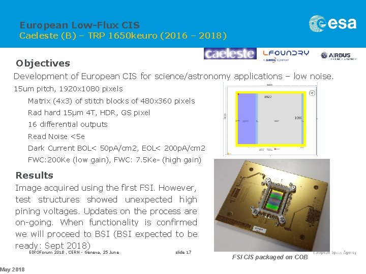
European Low-Flux CIS Caeleste (B) – TRP 1650 keuro (2016 – 2018) Objectives Development of European CIS for science/astronomy applications – low noise. 15 um pitch, 1920 x 1080 pixels Matrix (4 x 3) of stitch blocks of 480 x 360 pixels Rad hard 15μm 4 T, HDR, GS pixel 16 differential outputs Read Noise <5 e Dark Current BOL< 50 p. A/cm 2, EOL< 200 p. A/cm 2 FWC: 200 Ke (low gain), FWC: 7. 5 Ke- (high gain) Results Image acquired using the first FSI. However, test structures showed unexpected high pining voltages. Updates on the process are on-going. When functionality is confirmed we will proceed to BSI (BSI expected to be ready: Sept 2018) May 2018 EIROForum 2018 , CERN - Geneva, 25 June slide 17 FSI CIS packaged on COB
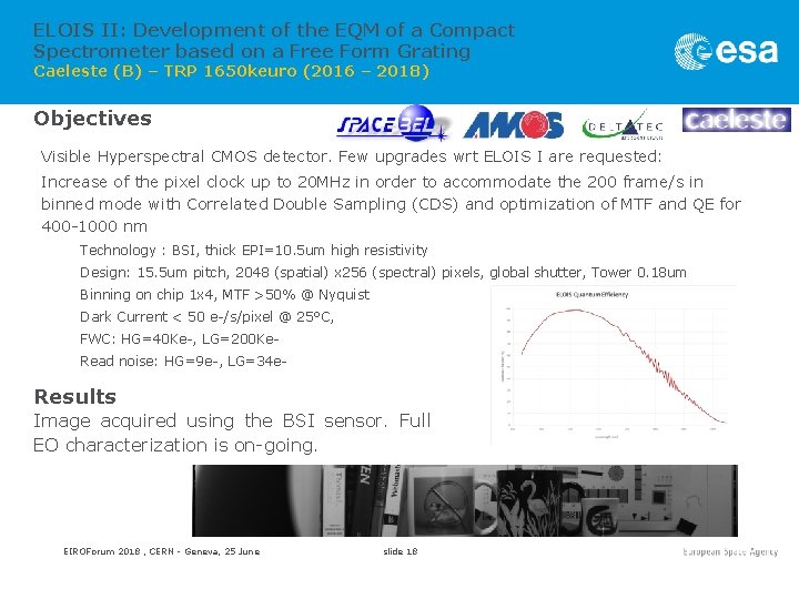
ELOIS II: Development of the EQM of a Compact Spectrometer based on a Free Form Grating Caeleste (B) – TRP 1650 keuro (2016 – 2018) Objectives Visible Hyperspectral CMOS detector. Few upgrades wrt ELOIS I are requested: Increase of the pixel clock up to 20 MHz in order to accommodate the 200 frame/s in binned mode with Correlated Double Sampling (CDS) and optimization of MTF and QE for 400 -1000 nm Technology : BSI, thick EPI=10. 5 um high resistivity Design: 15. 5 um pitch, 2048 (spatial) x 256 (spectral) pixels, global shutter, Tower 0. 18 um Binning on chip 1 x 4, MTF >50% @ Nyquist Dark Current < 50 e-/s/pixel @ 25°C, FWC: HG=40 Ke-, LG=200 Ke. Read noise: HG=9 e-, LG=34 e- Results Image acquired using the BSI sensor. Full EO characterization is on-going. EIROForum 2018 , CERN - Geneva, 25 June slide 18
Detector developments Hybrid Si CIS A number of advantages in the design and development of a hybrid CMOS image sensor – silicon photodiode layer bump-bonded to a silicon readout integrated circuit (ROIC) – have been identified • Separate optimisation of the photodiode and ROIC architecture • Photodiode design not limited by CMOS foundry • High fill-factor by default • Less parasitic light sensitivity • Increased options for detector manufacture within Europe EIROForum 2018 , CERN - Geneva, 25 June slide 19
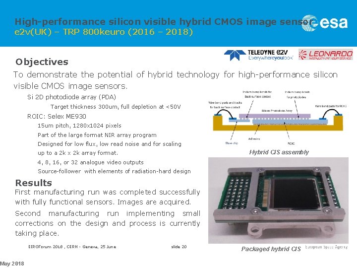
High-performance silicon visible hybrid CMOS image sensor e 2 v(UK) – TRP 800 keuro (2016 – 2018) Objectives To demonstrate the potential of hybrid technology for high-performance silicon visible CMOS image sensors. Si 2 D photodiode array (PDA) Target thickness 300 um, full depletion at <50 V ROIC: Selex ME 930 15 um pitch, 1280 x 1024 pixels Part of the large format NIR array program Designed for low flux, low read noise and for scaling Hybrid CIS assembly up to a 2 k x 2 k array format. 4, 8, 16, or 32 analogue video outputs Source-follower with elements of radiation-hard design Results First manufacturing run was completed successfully with fully functional sensors. Images are acquired. Second manufacturing run implementing small corrections on the design and process is currently taking place. May 2018 EIROForum 2018 , CERN - Geneva, 25 June slide 20 Packaged hybrid CIS
Second Generation APS for AOCS : HAS 3 On Semi (B) – GSTP 1700 keuro (2011– 2018) Objectives Two phase activity to prototype then qualify the future replacement for the HAS 2 (Detector for Star Trackers) APS detector. Key specs are : • 1280*1280 array, • 11 micron pitch, • 12 bit ADC, • custom hermetic package Results Detector functionality and performance is good. End user agreement currently needed with Israel to export the component. But power consumption is much higher than anticipated. May 2018 EIROForum 2018 , CERN - Geneva, 25 June slide 21
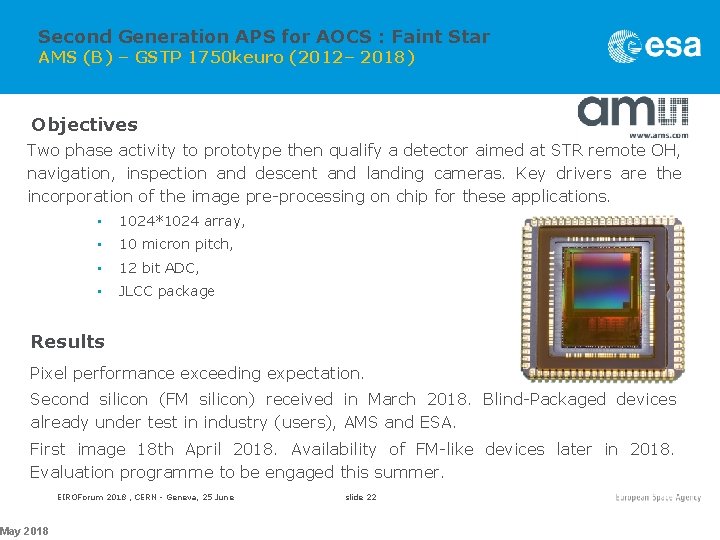
Second Generation APS for AOCS : Faint Star AMS (B) – GSTP 1750 keuro (2012– 2018) Objectives Two phase activity to prototype then qualify a detector aimed at STR remote OH, navigation, inspection and descent and landing cameras. Key drivers are the incorporation of the image pre-processing on chip for these applications. • 1024*1024 array, • 10 micron pitch, • 12 bit ADC, • JLCC package Results Pixel performance exceeding expectation. Second silicon (FM silicon) received in March 2018. Blind-Packaged devices already under test in industry (users), AMS and ESA. First image 18 th April 2018. Availability of FM-like devices later in 2018. Evaluation programme to be engaged this summer. May 2018 EIROForum 2018 , CERN - Geneva, 25 June slide 22
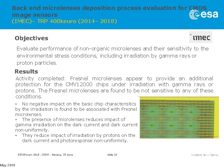
Back end microlenses deposition process evaluation for CMOS image sensors (IMEC)– TRP 400 keuro (2014– 2018) May 2018 Evaluate performance of non-organic microlenses and their sensitivity to the environmental stress conditions, including irradiation by gamma rays or proton particles. Activity completed: Fresnel microlenses appear to provide an additional protection for the CMV 12000 chips under irradiation with gamma rays or protons. The Fresnel microlenses are found to be not sensitive to any of these conditions. • No negative impact on the basic chip characteristics by the irradiation is found to be associated with Fresnel microlenses. • The presence of microlenses reduces impact of gamma irradiation on the dark current and dark current non-uniformity. • They reduce impact of irradiation by protons on the dark current and photoresponse non-uniformity. EIROForum 2018 , CERN - Geneva, 25 June slide 23
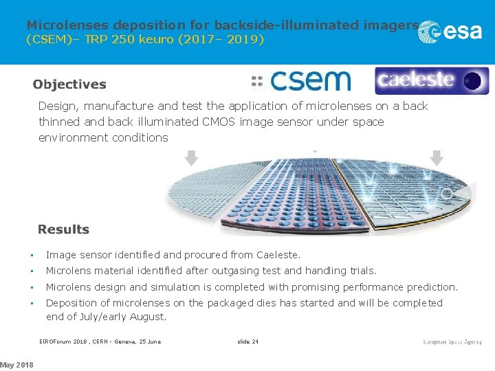
Microlenses deposition for backside-illuminated imagers (CSEM)– TRP 250 keuro (2017– 2019) Design, manufacture and test the application of microlenses on a back thinned and back illuminated CMOS image sensor under space environment conditions • Image sensor identified and procured from Caeleste. • Microlens material identified after outgasing test and handling trials. • Microlens design and simulation is completed with promising performance prediction. • Deposition of microlenses on the packaged dies has started and will be completed end of July/early August. May 2018 EIROForum 2018 , CERN - Geneva, 25 June slide 24
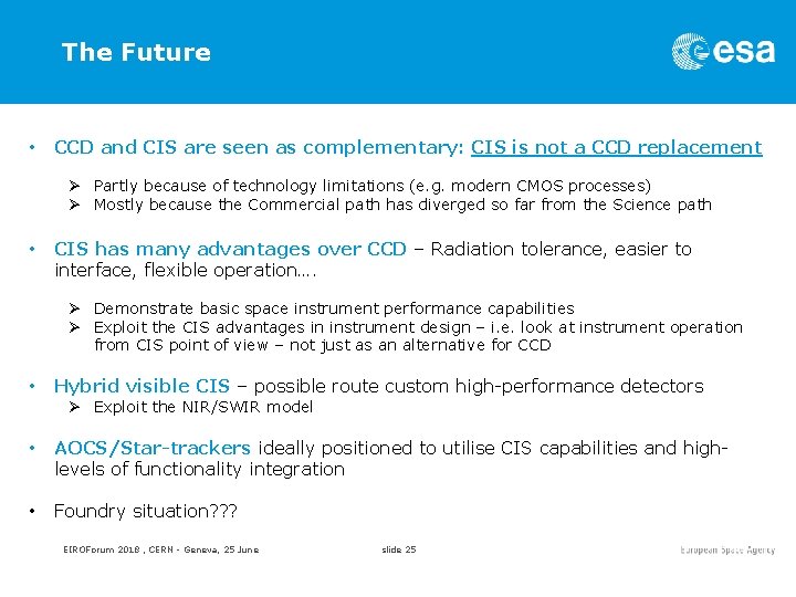
The Future • CCD and CIS are seen as complementary: CIS is not a CCD replacement Ø Partly because of technology limitations (e. g. modern CMOS processes) Ø Mostly because the Commercial path has diverged so far from the Science path • CIS has many advantages over CCD – Radiation tolerance, easier to interface, flexible operation…. Ø Demonstrate basic space instrument performance capabilities Ø Exploit the CIS advantages in instrument design – i. e. look at instrument operation from CIS point of view – not just as an alternative for CCD • Hybrid visible CIS – possible route custom high-performance detectors • AOCS/Star-trackers ideally positioned to utilise CIS capabilities and highlevels of functionality integration • Foundry situation? ? ? Ø Exploit the NIR/SWIR model EIROForum 2018 , CERN - Geneva, 25 June slide 25
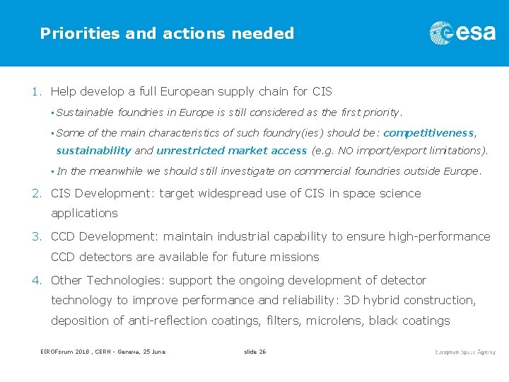
Priorities and actions needed 1. Help develop a full European supply chain for CIS • Sustainable foundries in Europe is still considered as the first priority. • Some of the main characteristics of such foundry(ies) should be: competitiveness, sustainability and unrestricted market access (e. g. NO import/export limitations). • In the meanwhile we should still investigate on commercial foundries outside Europe. 2. CIS Development: target widespread use of CIS in space science applications 3. CCD Development: maintain industrial capability to ensure high-performance CCD detectors are available for future missions 4. Other Technologies: support the ongoing development of detector technology to improve performance and reliability: 3 D hybrid construction, deposition of anti-reflection coatings, filters, microlens, black coatings EIROForum 2018 , CERN - Geneva, 25 June slide 26
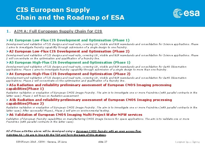
CIS European Supply Chain and the Roadmap of ESA 1. AIM A: Full European Supply Chain for CIS ØA 1 European Low-Flux CIS Development and Optimisation (Phase 1) Development and validation of CIS designs and read-outs, covering UV, visible and NIR wavebands and consolidation for Science applications. Phase 1 aims to investigate foundry capability through submission of a single design to one foundry. ØA 2 European Low-Flux CIS Development and Optimisation (Phase 2) Development and validation of CIS designs and read-outs, covering UV, visible and NIR wavebands and consolidation for Science applications. Phase 2 will concentrate on the optimisation and qualification of a foundry line. ØA 3 European High-Flux CIS Development and Optimisation (Phase 1) Development and validation of CIS designs and read-outs, covering UV, visible and NIR wavebands and consolidation for Earth Observation applications. Phase 1 aims to investigate foundry capability through submission of a single design to more than one foundry. ØA 4 European High-Flux CIS Development and Optimisation (Phase 2) Development and validation of CIS designs and read-outs, covering UV, visible and NIR wavebands and consolidation for Earth Observation applications. Phase 2 will concentrate on the optimisation and qualification of a foundry line. ØA 5 a Radiation and reliability preliminary assessment of European CMOS Imaging processing capabilities(Phase 1) Radiation validation or evaluation of European CMOS Image Foundry. The aim is to investigate one or more Foundries (with parallel contracts in the latter case). Phase 1 will focus on Radiation assessment Ø A 5 b Radiation and reliability preliminary assessment of European CMOS Imaging processing capabilities(Phase 2) Radiation validation or evaluation of European CMOS Image Foundry. The aim is to investigate one or more Foundries (with parallel contracts in the latter case). After successful Phase 1, Phase 2 will aim on environmental testing. ØA 6 Validation of European CMOS Imaging Multi Project Wafer MPW services Validation of European Foundry capabilities on manufacturing CMOS Image Sensors for space applications. The aim is to validate one or more Foundries (with parallel contracts in the latter case). All of these activities above will be developed using a European CMOS foundry with an open access flow. Activities A 1 – A 6 are in line with the TDP and form the basis of this strategy. EIROForum 2018 , CERN - Geneva, 25 June slide 27
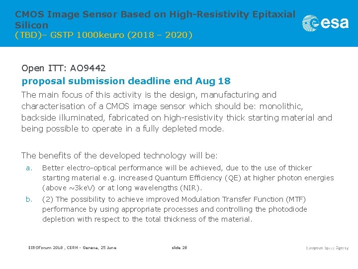
CMOS Image Sensor Based on High-Resistivity Epitaxial Silicon (TBD)– GSTP 1000 keuro (2018 – 2020) Open ITT: AO 9442 proposal submission deadline end Aug 18 The main focus of this activity is the design, manufacturing and characterisation of a CMOS image sensor which should be: monolithic, backside illuminated, fabricated on high-resistivity thick starting material and being possible to operate in a fully depleted mode. The benefits of the developed technology will be: a. Better electro-optical performance will be achieved, due to the use of thicker starting material e. g. increased Quantum Efficiency (QE) at higher photon energies (above ~3 ke. V) or at long wavelengths (NIR). b. (2) The possibility to achieve improved Modulation Transfer Function (MTF) performance by using appropriate processes and controlling the photodiode depletion with respect to the total thickness of the material. EIROForum 2018 , CERN - Geneva, 25 June slide 28
Take home message 1. ESA is aiming on high performance detectors 2. CIS are an essential part of the detector development strategy 3. CIS is seen as complementary to CCD, not a replacement 4. The Agency recognizes the importance of not only improving and optimizing the performance of detectors but also in supporting their continued availability 5. Related R&D activities are on-going, more are included in the Roadmap EIROForum 2018 , CERN - Geneva, 25 June slide 29
With the inputs of: N. Nelms A. Ciapponi H. Weber S. Wittig B. Leone P. Crouzet S. Kowaltzek Thank you! EIROForum 2018 , CERN - Geneva, 25 June slide 30

More slides….
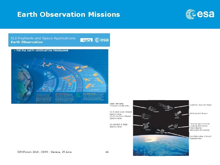
Earth Observation Missions EIROForum 2018 , CERN - Geneva, 25 June slide 32
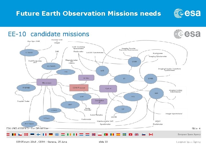
Future Earth Observation Missions needs EIROForum 2018 , CERN - Geneva, 25 June slide 33
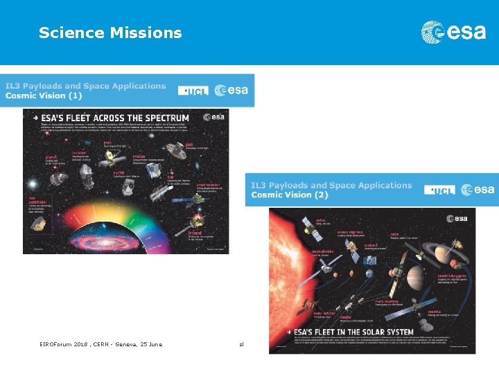
Science Missions EIROForum 2018 , CERN - Geneva, 25 June slide 34
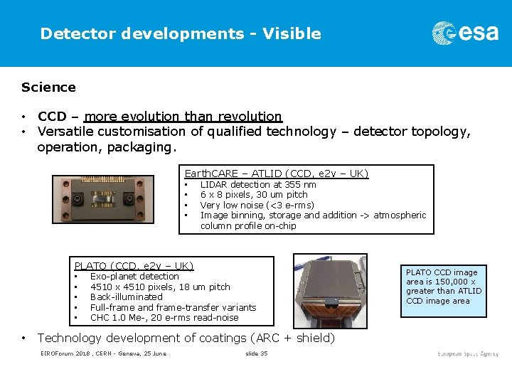
Detector developments - Visible Science • CCD – more evolution than revolution • Versatile customisation of qualified technology – detector topology, operation, packaging. Earth. CARE – ATLID (CCD, e 2 v – UK) • • LIDAR detection at 355 nm 6 x 8 pixels, 30 um pitch Very low noise (<3 e-rms) Image binning, storage and addition -> atmospheric column profile on-chip PLATO (CCD, e 2 v – UK) • • • Exo-planet detection 4510 x 4510 pixels, 18 um pitch Back-illuminated Full-frame and frame-transfer variants CHC 1. 0 Me-, 20 e-rms read-noise Technology development of coatings (ARC + shield) EIROForum 2018 , CERN - Geneva, 25 June slide 35 PLATO CCD image area is 150, 000 x greater than ATLID CCD image area
- Slides: 35