CMOS FABRICATION PROCESS Processes used in fabrication Crystal

CMOS FABRICATION PROCESS
Processes used in fabrication Crystal Growth Oxidation Lithography Diffusion Implantation Etching Chemical Vapour Deposition Metallization
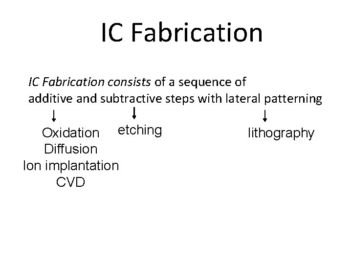
IC Fabrication consists of a sequence of additive and subtractive steps with lateral patterning Oxidation etching Diffusion Ion implantation CVD lithography
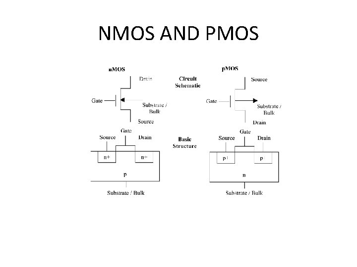
NMOS AND PMOS
NMOS Fabrication
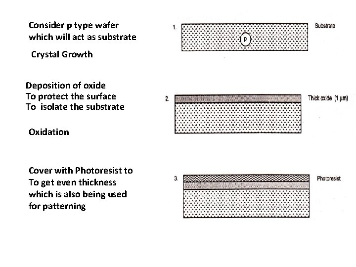
Consider p type wafer which will act as substrate Crystal Growth Deposition of oxide To protect the surface To isolate the substrate Oxidation Cover with Photoresist to To get even thickness which is also being used for patterning
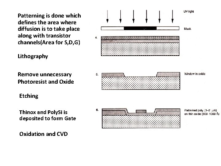
Patterning is done which defines the area where diffusion is to take place along with transistor channels(Area for S, D, G) Lithography Remove unnecessary Photoresist and Oxide Etching Thinox and Poly. Si is deposited to form Gate Oxidation and CVD
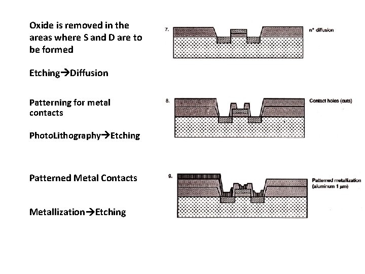
Oxide is removed in the areas where S and D are to be formed Etching Diffusion Patterning for metal contacts Photo. Lithography Etching Patterned Metal Contacts Metallization Etching
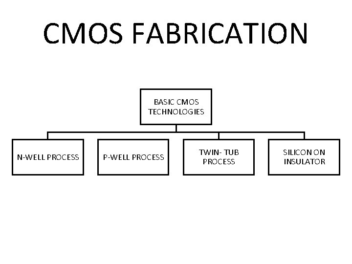
CMOS FABRICATION BASIC CMOS TECHNOLOGIES N-WELL PROCESS P-WELL PROCESS TWIN- TUB PROCESS SILICON ON INSULATOR

N-Well Process
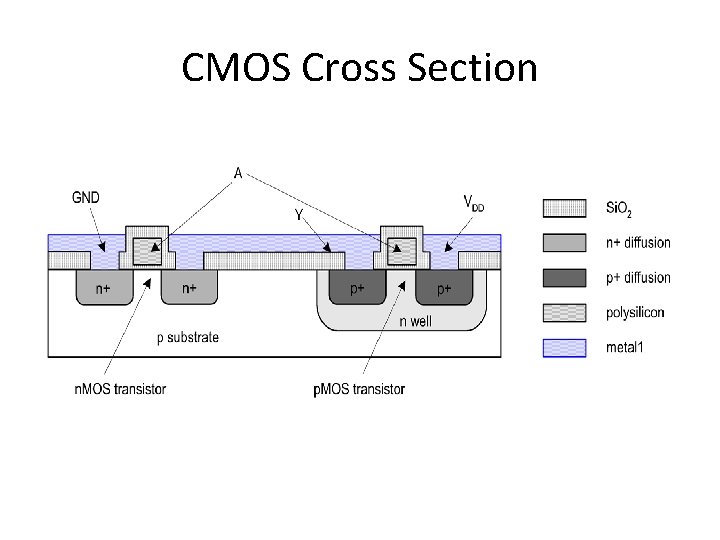
CMOS Cross Section
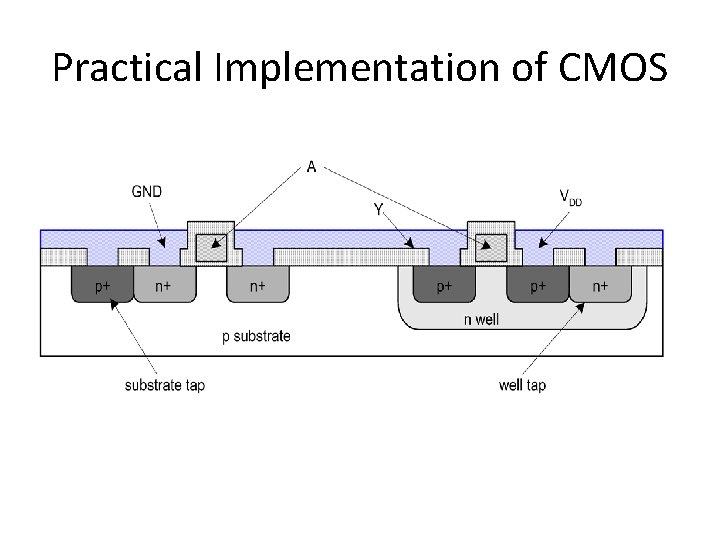
Practical Implementation of CMOS
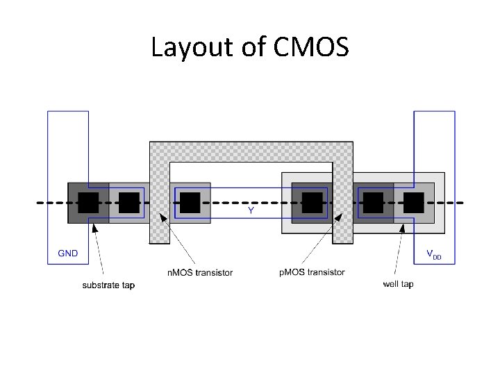
Layout of CMOS
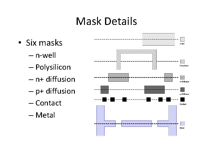
Mask Details • Six masks – n-well – Polysilicon – n+ diffusion – p+ diffusion – Contact – Metal
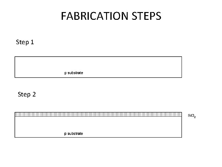
FABRICATION STEPS Step 1 Step 2
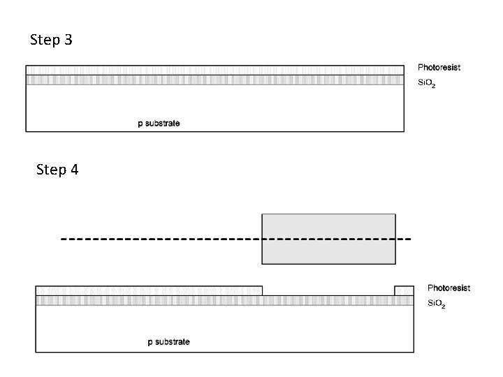
Step 3 Step 4
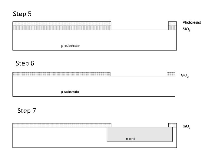
Step 5 Step 6 Step 7

Step 8 Step 9
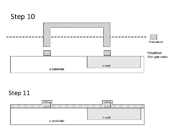
Step 10 Step 11
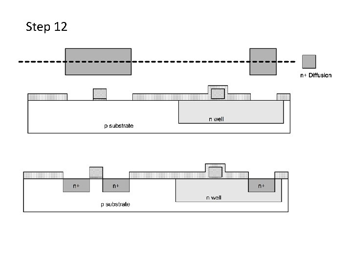
Step 12
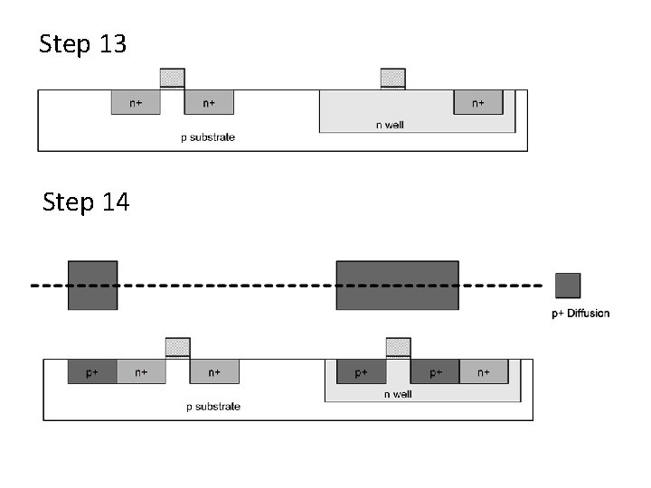
Step 13 Step 14
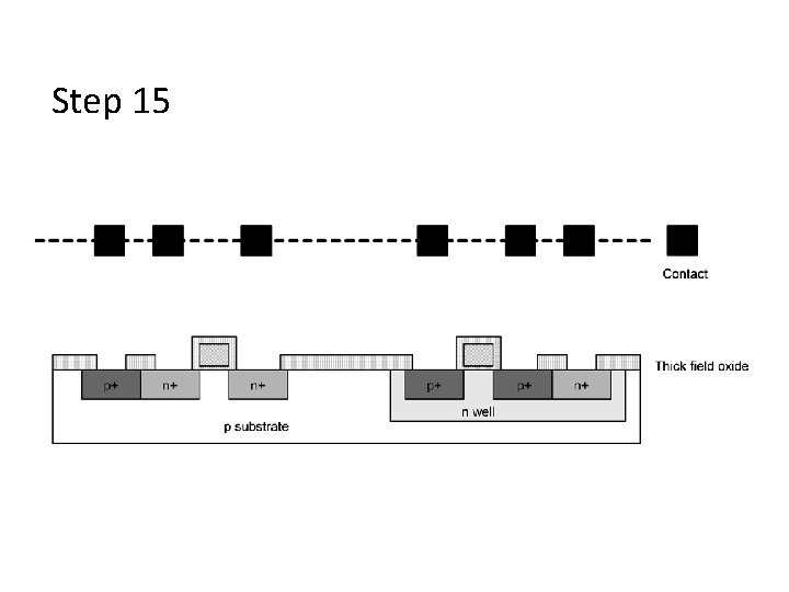
Step 15
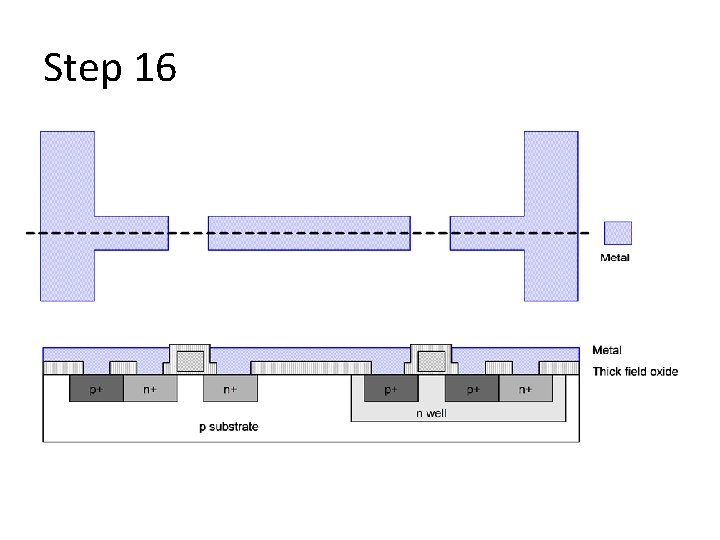
Step 16

Step 17 Step 18
P WELL PROCESS 1)Same procedure as N-Well 2)Main substrate is n type 3)P-Well should be formed
Advanced CMOS Fabrication Processes 1)Twin Tub Process 2)Si on Insulator(SIO) Process
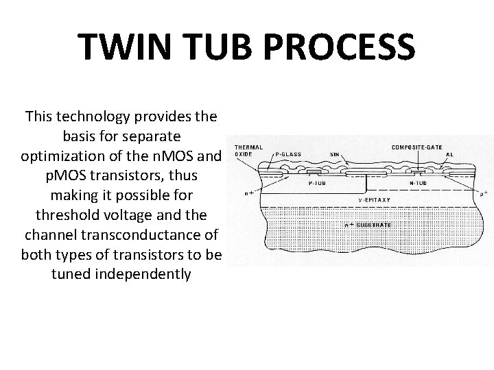
TWIN TUB PROCESS This technology provides the basis for separate optimization of the n. MOS and p. MOS transistors, thus making it possible for threshold voltage and the channel transconductance of both types of transistors to be tuned independently
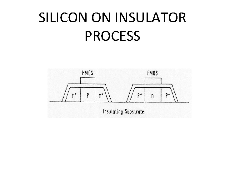
SILICON ON INSULATOR PROCESS
No Well formation so high integration density Rather than using Si as substrate, insulating substrate is used to deal with speed requirements No parasitic capacitances between S/D and body, so leakage current is less, thus faster speed

- Slides: 30