CMOS FABRICATION By Joaquin Gabriels November 24 th
CMOS FABRICATION By: Joaquin Gabriels November 24 th, 2008
Outline Overview of CMOS Fabrication Process Overview CMOS Fabrication Process Problems with Current CMOS Fabrication Future Changes in CMOS Fabrication
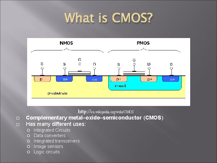
What is CMOS? http: //en. wikipedia. org/wiki/CMOS Complementary metal–oxide–semiconductor (CMOS) Has many different uses: Integrated Circuits Data converters Integrated transceivers Image sensors Logic circuits
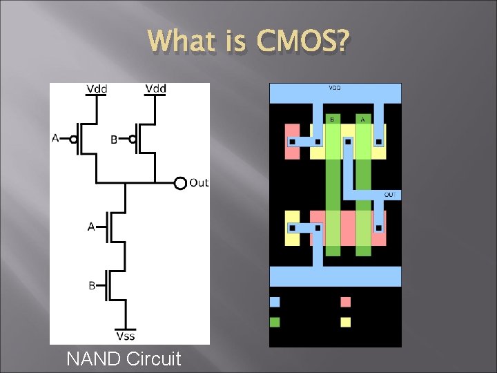
What is CMOS? NAND Circuit
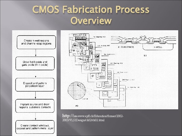
CMOS Fabrication Process Overview http: //lsmwww. epfl. ch/Education/former/20022003/VLSIDesign/ch 02. html
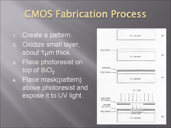
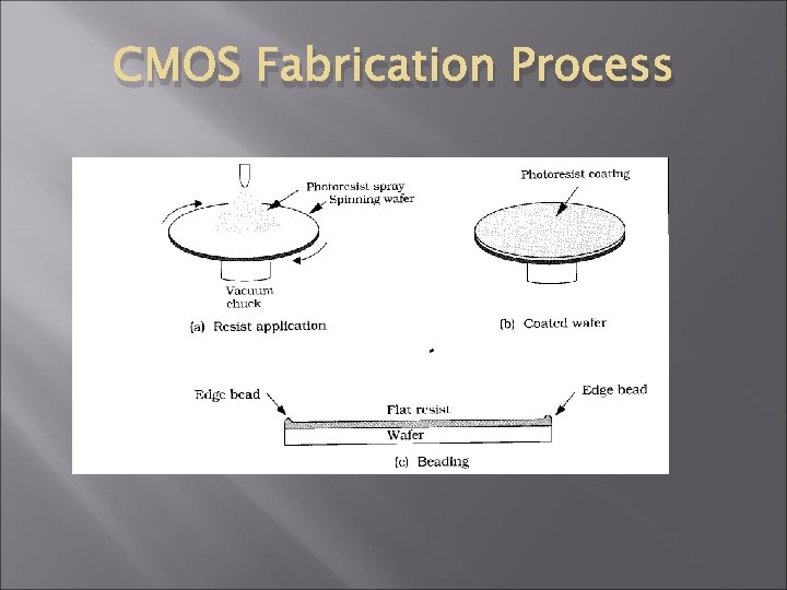
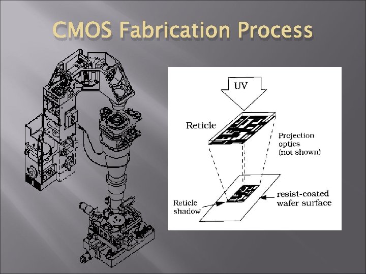
CMOS Fabrication Process 1. 2. 3. 4. Create a pattern. Oxidize small layer, about 1µm thick. Place photoresist on top of Si. O 2 Place mask(pattern) above photoresist and expose it to UV light.
CMOS Fabrication Process
CMOS Fabrication Process
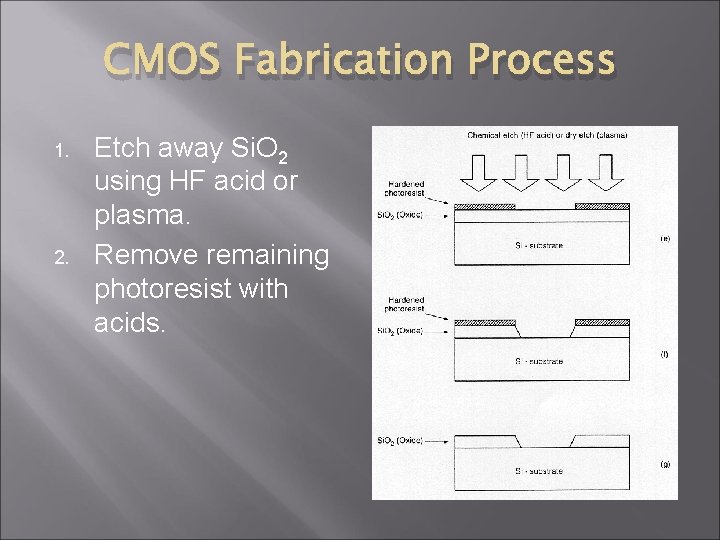
CMOS Fabrication Process 1. 2. Etch away Si. O 2 using HF acid or plasma. Remove remaining photoresist with acids.
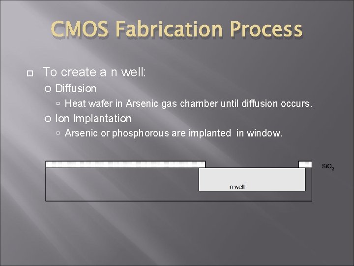
CMOS Fabrication Process To create a n well: Diffusion Heat wafer in Arsenic gas chamber until diffusion occurs. Ion Implantation Arsenic or phosphorous are implanted in window.

CMOS Fabrication Process

CMOS Fabrication Process A thin layer of oxide is deposited. A thin layer of polysilicon is deposited using Chemical Vapor Deposition (CVD).

CMOS Fabrication Process http: //en. wikipedia. org/wiki/Chemical_vapor_deposition

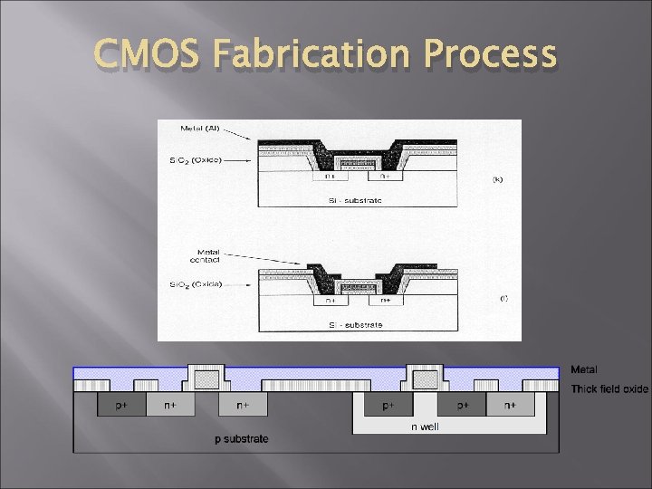
CMOS Fabrication Process Remove oxide layer using acid. Dope open area using Ion implantation or diffusion.
CMOS Fabrication Process
CMOS Fabrication Process

Problems with Current CMOS Fabrication Optical lithography is limited by the light frequency. Material limitations Yield limitations Space limitations
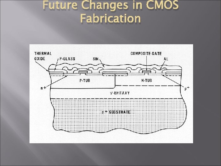
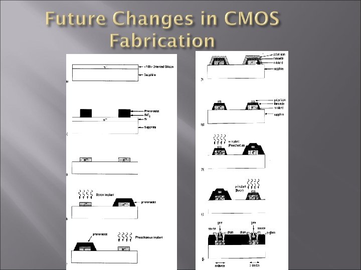
Future Changes in CMOS Fabrication Material changes like using high-k materials. Design changes SOI(Silicon On Insulator) Double Gate (Finfet) Twin-Tub Process
Future Changes in CMOS Fabrication

Future Changes in CMOS Fabrication
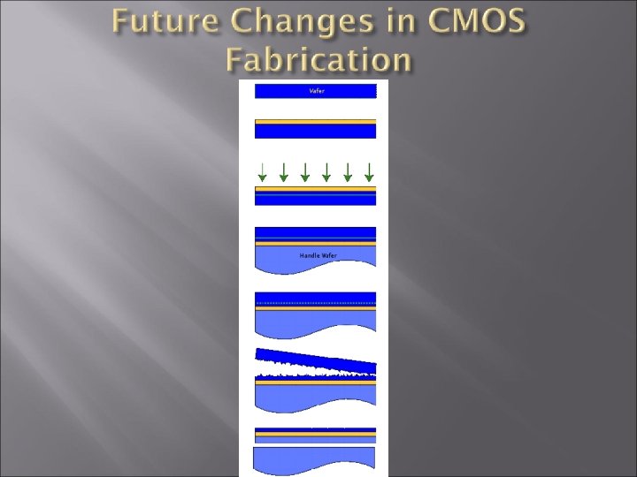
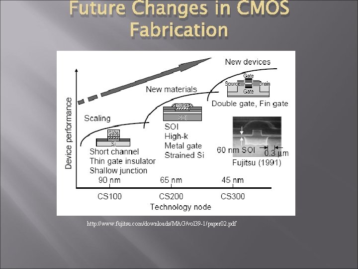
Future Changes in CMOS Fabrication http: //www. fujitsu. com/downloads/MAG/vol 39 -1/paper 02. pdf
References CMOS Digital Integrated Circuit Design - Analysis and Design by S. M. Kang and Y. Leblebici http: //www. fujitsu. com/downloads/MAG/vol 39 -1/paper 02. pdf “Introduction to VLSI Circuits and Systems, ” John Wiley and Sons, 2002 http: //lsmwww. epfl. ch/Education/former/20022003/VLSIDesign/ch 02. html http: //en. wikipedia. org/wiki/Chemical_vapor_deposition users. ece. utexas. edu/~adnan/vlsi-05/lec 0 Fab. ppt http: //en. wikipedia. org/wiki/CMOS www. usna. edu/EE/ee 452/Lecture. Notes/02_CMOS_Process_Steps/08_Simple_CMOS_Fab. ppt http: //en. wikipedia. org/wiki/Silicon_on_insulator access. ee. ntu. edu. tw/course/VLSI_design_90 second/data/Chapter%203 %20 Part 2%2003 -20 -2002. doc
- Slides: 24