CMOS Devices PN junctions and diodes NMOS and


≈ gm/Cgs")


 – BSIM 3, BSIM 4 models")


 vs VG is sensitive to VBS")

 has fixed shape")


- Slides: 89
CMOS Devices • • • PN junctions and diodes NMOS and PMOS transistors Resistors Capacitors Inductors Bipolar transistors
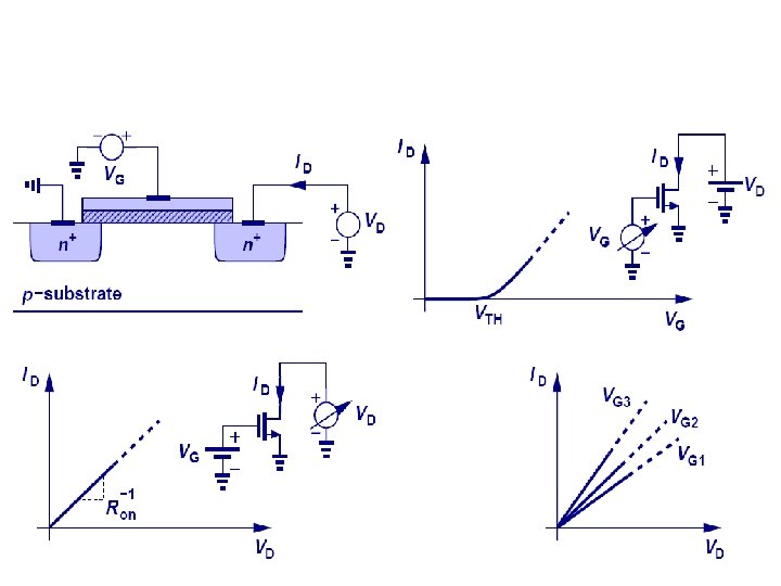
The MOS Transistors
The MOS Transistors
CMOS Device Model • Objective – Hand calculations for analog design – Non-idealities and their effects – Efficient and accurate simulation • CMOS transistor models – Large signal model – Small signal model – Simulation model – Noise model
Large Signal Model • Nonlinear equations for solving dc values of device currents, given voltages • Level 1: Shichman-Hodges (VT, K', g, l, f, and NSUB) • Level 2: with second-order effects (varying channel charge, short-channel, weak inversion, varying surface mobility, etc. ) • Level 3: Semi-empirical short-channel model • Level 4: BSIM models. Based on automatically generated parameters from a process characterization. Good weak-strong inversion transition.
Gate contact is always placed off gate area! Device is symmetric. Higher voltage side is drain, lower voltage side is source. BSIM 5 and PSP models will enforce this symmetry.
Transconductance when VDS is small This shows when VGS=0. As VGS , depletion region appears under gate oxide. When VGS=VT, an inversion layer begins to appear under gate oxide. This is sub-threshold.
Sub-threshold • PN junction depletion region completely surrounds drain area and source area • Current from D to S is nearly 0 • Tiny diode currents come out of drain and out of source • PN junction at D is more negatively biased, so less diode current out of D • So net positive current from D to S
Sub-threshold • Diode current is exponential function of PN junction voltage • When VGS not =0, PN junction voltage not uniform • Highest PN junction voltage happens near the corner by the gate
Transconductance when VDS is small
Voltage controlled resistor and attenuator
Non-uniform channel potential non-uniform gate-substrate voltage and non-uniform threshold voltage
Good for VDS <VGS -VTH After that, ID become saturated.
Linear in deep triode Pro: voltage control of resistivity. Con: nonlinear resistor.
MOST Regions of Operation • Cut-off, or non-conducting: v. GS <VT – i. D=0 approximately • Conducting, or on: v. GS >=VT – Saturation: v. DS > v. GS – VT – Triode or linear or ohmic or non-saturation: v. DS <= v. GS – VT
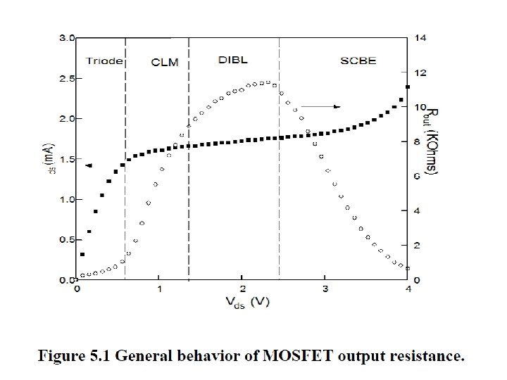
With channel length modulation
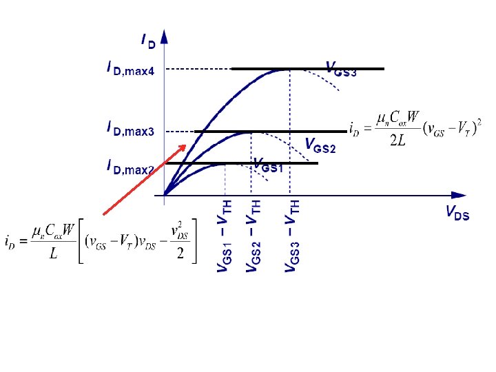
i. D vs v. GS for several VDS Square function But when v. GS-VT > VDS: Straight line
i. D vs v. DS for several VGS gds gm*DVGS
i. D vs v. DS for several VGS -VA
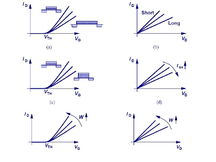
Influence of Channel Length on l Lmin = 0. 25 Johns and Martin book gives an approximate formula with l 1/L At >=2*Lmin, l is small, Ro is large After 1 um, l remains about the same
Influence of VBS changes threshold voltage, and hence changes i-v curve.
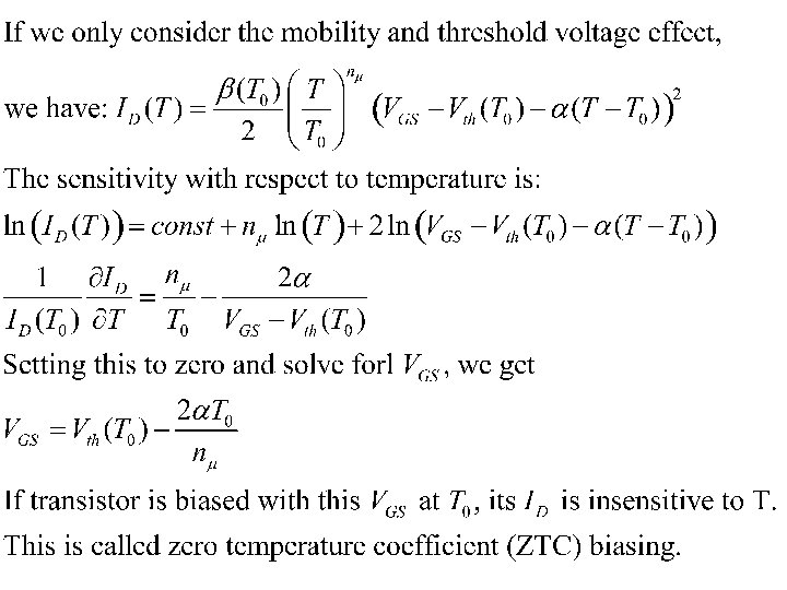
Temperature Dependence of Mobility Linear Temperature Dependence of threshold voltage Saturation Velocity Junction capacitance Barrier potential
This is nonlinear if Vbs is temperature dependent
Typical VT and ß temperature performance VT ß Temp
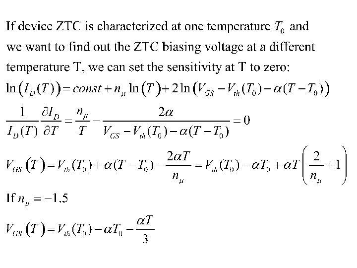
0. 35 um process ZTC biasing Referenced from Filanovsky’s paper
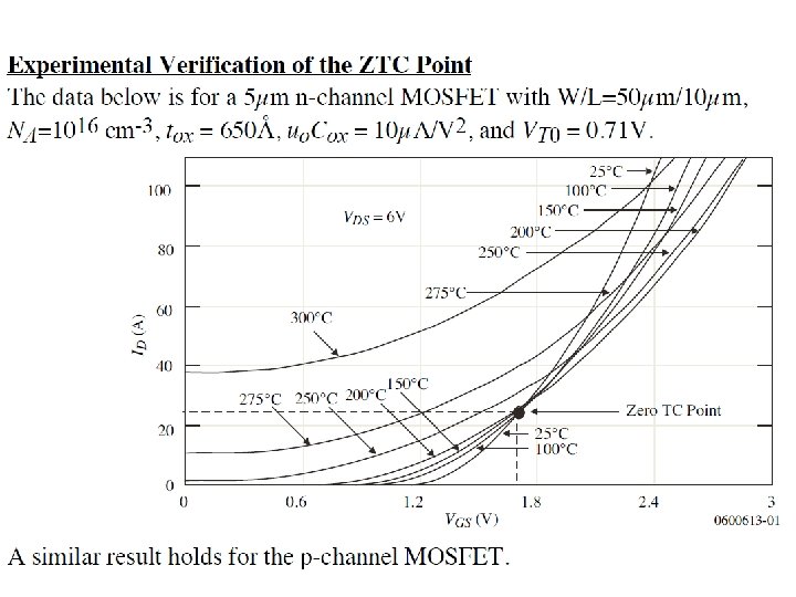
Reality: no single point crossing ID Not just one single crossing In AMI 0. 6 process Test on a single NMOS biased with fixed Vgs and Vds Vgs
AMI 0. 6 To refine the value. Vgs=1. 12 V Vgs=1. 14 V Optimum curve TC = 41 ppm/C Vgs=1. 17 V
Generic 018 Vgs=0. 717 V TC=27 ppm/C Vgs=0. 721 V Vgs=0. 727 V
Large signal model for approximate hand ca; culation
Capacitors Of The MOSFET
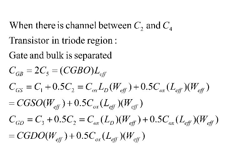
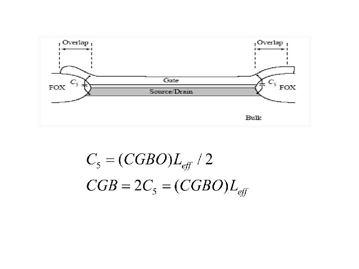
C 2 is the capacitance between the gate and the channel. C 2 is not directly measurable. C 4 is the capacitance between the channel and the bulk. It is highly nonlinear and depends on the operation of the device. C 4 is not measurable from terminals. C 2 and C 4 in series give part of CGB that can be measurable.
CBD and CBS include both the diffusion-bulk junction capacitance as well as the side wall junction capacitance. They are highly nonlinear in bias voltages.
Gate related capacitances
Capacitors in Cutoff
Capacitors in Saturation
Capacitors in Triode
Small signal model
Typically: VDB, VSB are in such a way that there is a reversely biased pn junction. Therefore: gbd ≈ gbs ≈ 0
In saturation: But
Intrinsic DC voltage gain: gm/gds = gm*rds
In non-saturation region
Transistor performance • Intrinsic gain • Speed / bandwidth • gm efficiency • • Linearity Area, Power Matching
Intrinsic gain For large gain, use small ID or small over drive voltage, or in moderate to weak inversion.
High Frequency Figure of Merit w. T • • • AC current source input to G AC short S, D, B to gnd (i. e. constant voltages) Measure AC drain current output Calculate current gain Find frequency at which current gain = 1. Ignore rs and rd, Cbs, Cbd, gds, gbd all have zero voltage drop and hence zero current • Vgs = Iin /jw(Cgs+Cgb+Cgd) ≈ Iin /jw(Cgs+Cgd) • Io = − (gm − jw. Cgd)Vgs ≈ − gm Iin /jw(Cgs+Cgd) • |Io/Iin| = |gm − jw. Cgd|/w(Cgs+Cgd) ≈ gm/w(Cgs+Cgd)
amplification |Io/Iin| 0 d. B attenuation w. T w
• At w. T, current gain =1 • w. T ≈ gm/(Cgs+Cgd)≈ gm/Cgs • or
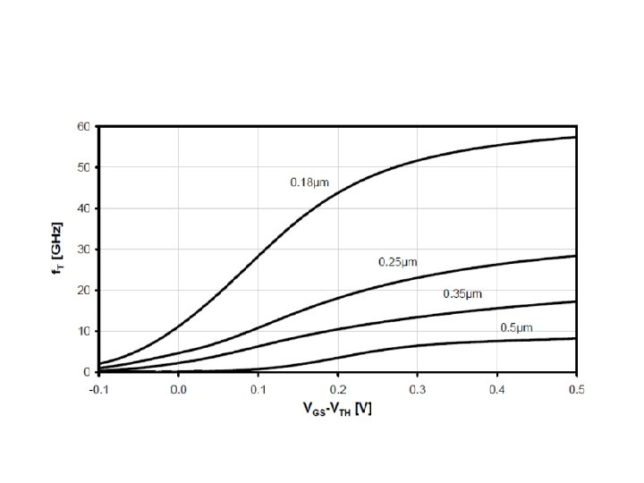
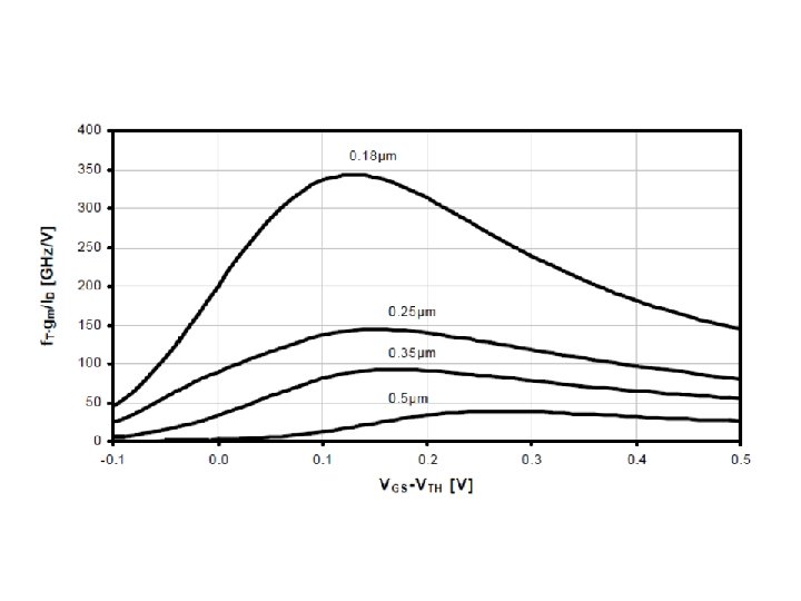
For fastest operation, use Vod near but before f. T peak For power efficiency, use Vod before f. T corner
High Frequency Figures of Merit wmax • • AC current source input to G AC short S, B to gnd Measure AC power into the gate Assume complex conjugate load Compute max power delivered by the transistor Find maximum power gain Find frequency at which power gain = 1.
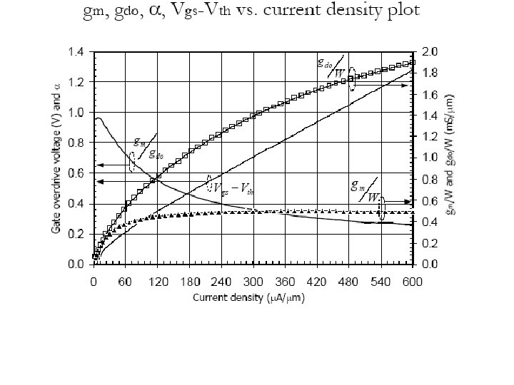
gdo vs gm in short channel
gdo vs gm in short channel
Insights: • gdo increases all the way with current density Iden • gm saturates when Iden larger than 100 m. A/mm – Velocity saturation, mobility degradation ---short channel effects – Low gm/current efficiency – High linearity • For power efficiency and gm efficiency – Use moderate to low current density – Use small over drive voltage
BSIM models • Non-uniform charge density • Band bending due to non-uniform gate voltage • Non-uniform threshold voltage – Non-uniform channel doping, x, y, z – Short channel effects • Charge sharing • Drain-induced barrier lowering (DIBL) – Narrow channel effects – Temperature dependence • Mobility change due to temp, field (x, y) • Source, drain, gate, bulk resistances
“Short Channel” Effects • VTH decreases for small L – Large offset for diff pairs with small L • Mobility reduction: – Velocity saturation – Vertical field (small tox=6. 5 nm) – Reduced gm: increases slower than root-ID
Threshold Voltage VTH • Strong function of L – Use long channel for VTH matching – But this increases cap and decreases speed • Process variations – Run-to-run – How to characterize? – Slow/nominal/fast – Both worst-case & optimistic
Effect of Velocity Saturation • Velocity ≈ mobility * field • Field reaches maximum Emax – (Vgs-Vt)/L reaches ESAT • gm become saturated: – gm ≈ ½mn. Cox. W*ESAT • But Cgs still 2/3 WL Cox • w. T ≈ gm/Cgs = ¾ mn. ESAT /L • No longer ~ 1/L^2
Threshold Reduction • When channel is short, effect of Vd extends to S • Cause barrier to drop, i. e. Vth to drop • Greatly affects sub-threshold current: 26 m. V Vth drop current * e • 100~200 m. V Vth drop due to Vd not uncommon 100’s or 1000 times current increase • Use lower density active near gate but higher density for contacts
Other effects • Temperature variation • Normal-Field Mobility Degradation • Substrate current – Very nonlinear in Vd • Drain to source leakage current at Vgs=0 – Big concern for static power • Gate leakage currents – Hot electron – Tunneling – Very nonlineary • Transit Time Effects
Consequences for Design • SPICE (HSPICE or Spectre) – BSIM 3, BSIM 4 models – Accurate but inappropriate for hand analysis – Verification (& optimization) • Design: – Small signal parameter design space: • gm , C L • gm/ID, ID • Av 0= gmro (speed, noise) (power, output range, speed) (gain) – Device geometries from SPICE (table, graph); – may require iteration (e. g. CGS)
Intrinsic voltage gain of MOSFET Sweep V 1 Measure vgs Intrinsic voltage gain = gm/go = Dvds/Dvgs for constant Id
Intrinsic voltage gain of MOSFET Sweep V 1 Measure vgs + + Intrinsic voltage gain = gm/go = Dvds/Dvgs for constant Id
Weak inversion • When VGS is reduced to Vth, the drain current does not go to zero – It does not follow square law – It does not follow exponential law • When VGS is markedly below Vth, the drain current becomes an exponential function of VGS. – Behaves very much like a diode
A model from weak to strong inv
In strong inversion, n is about 1
In weak inversion
In weak inversion If vt = 25 m. V, n=2, gm/ID = 20 n=1. 5, gm/ID = 27 n=1. 2, gm/ID = 33
ID vs VGS Exponential model Square law model simulation
ID/(W/L) vs VG is sensitive to VBS
gm/ID vs VG is also sensitive to VBS
But gm/ID vs ID/(W/L) has fixed shape
Related VDD insensitive circuits • Filanovsky, etc, “Mutual Compensation of Mobility and Threshold Voltage Temperature Effects with Applications in CMOS Circuits”. • G. Giustolisi “A Low-Voltage Low-Power Voltage Reference Based on Subthreshold MOSFETs”. • Ka Nang Leung “A CMOS Voltage Reference Based on Weighted VGS for CMOS Low-Dropout Linear Regulators”. • Bernhard Boser. “Analog Circuit Design with Submicron Transistors". IEEE SSCS Meeting, Santa Clara Valley, May 2005.
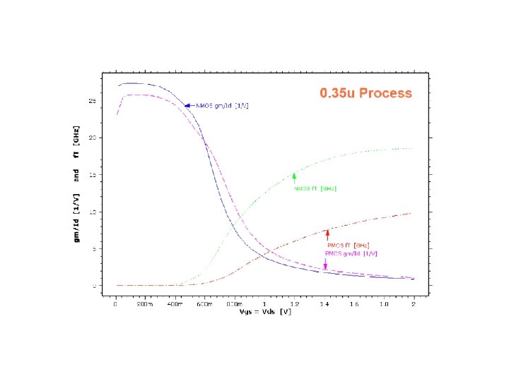
TSMC 0. 18 um Process
TSMC 0. 18 um Process
TSMC 0. 18 um Process
TSMC 0. 18 um Process
TSMC 0. 18 um Process
TSMC 0. 18 um Process