CMOS Devices PN junctions and diodes NMOS and


 of a capacitor 2. Parasitic capacitors to ground")


- Slides: 52
CMOS Devices • • • PN junctions and diodes NMOS and PMOS transistors Resistors Capacitors Inductors Bipolar transistors
PN Junctions Charges on two sides equal but opposite sign.
PN Junctions Depletion region widths: Built-in potential:
PN Junctions The depletion charge The junction capacitance
• Can be used as voltage controlled capacitor • Here m = 1/2 for the step change in impurity concentration. • For gradual concentration change, m = 1/3. Real case is somewhere in between. mj and Cj 0 per unit area can be found from the pdk.
Impurity concentration profile for diffused pn junction
Current density at boundary due to holes: Total: Diode current:
The MOS Transistors
Capacitors • Two conductor plates separated by an insulator form a capacitor • Intentional capacitors vs parasitic capacitors • Linear vs nonlinear capacitors Linear capacitors: Non-linear:
Capacitor specifications 1. Dissipation (quality factor) of a capacitor 2. Parasitic capacitors to ground from each node of the capacitor. 3. The density of the capacitor in Farads/area. 4. The absolute and relative accuracies of the capacitor. 5. The Cmax/Cmin ratio which is the largest value of capacitance to the smallest when the capacitor is used as a variable capacitor (varactor). 6. The variation of a variable capacitance with the control voltage (is it linear). 7. Linearity, q = Cv.
PMOS on Substrate Gate Capacitors High density, good matching, but nonlinear
NMOS in p-well Gate Capacitor • Gate as one terminal of the capacitor • Some combination of the source, drain, and bulk as the other terminal
Gate Capacitor vs. VGS with D=S=B
3 -seg Approximation
Gate Capacitor in Inversion Mode VSS
Inversion Mode NMOS Capacitor E. Pedersen, “RF CMOS Varactors for 2 GHz Applications, ” Analog Integrated Circuits and Signal Processing, vol. 26, pp. 27 -36, Jan. 2001.
PN Junction Capacitors in a Well
PN-Junction Capacitors E. Pedersen, “RF CMOS Varactors for 2 GHz Applications, ” Analog Integrated Circuits and Signal Processing, vol. 26, pp. 27 -36, Jan. 2001.
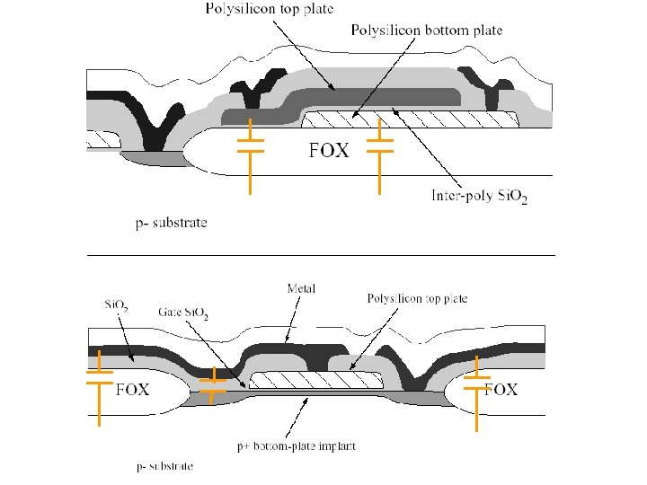
Poly-poly cap on FOX High density, good matching, good linearity, but require two-poly processes
Poly-poly cap on STI • Very linear • Small bottom plate parasitics
Metal-insulator-metal cap
Fringe Capacitors
R. Aparicio and A. Hajimiri, “Capacity Limits and Matching Properties of Integrated Capacitors, ” IEEE J. of Solid-State Circuits, vol. 37, no. 3, March 2002, pp. 384 -393.
Comparison
Non-ideal Behavior • • • Dielectric gradients Edge effects Process biases Parasitics Voltage dependence Temperature dependence
Parasitic Capacitors
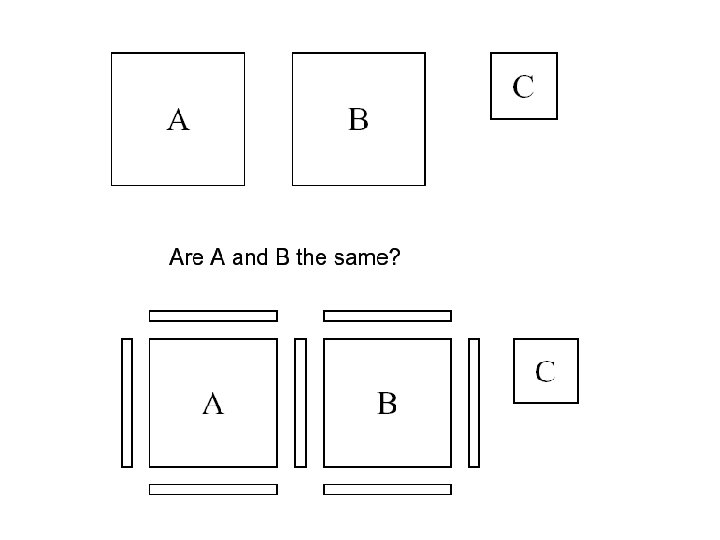
Proper layout of capacitors For achieving CA = 2 CB, which one is better?
Various Capacitor Errors
Temperature and Voltage Dependence • MOSFET Gate Capacitors: – – Absolute accuracy ≈ ± 10% Relative accuracy ≈ ± 0. 2% Temperature coefficient ≈ +25 ppm/C° Voltage coefficient ≈ -50 ppm/V • Polysilicon-Oxide-Polysilicon Capacitors: – – Absolute accuracy ≈ ± 10% Relative accuracy ≈ ± 0. 2% Temperature coefficient ≈ +25 ppm/C° Voltage coefficient ≈ -20 ppm/V • Metal-Dielectric-Metal Capacitors: – Absolute accuracy ≈ ± 10% – Relative accuracy ≈ ± 0. 6% – Temperature coefficient ≈ +40 ppm/C° – Voltage coefficient ≈ -20 ppm/V, 5 ppm/V 2 • Accuracies depend upon the size of the capacitors.
Improving Cap Matching • Divide each cap into even # of unit caps • Each unit cap is square, has identical construction, has identical vicinity, has identical routing • The unit caps for match critical caps are laid out with inter-digitation, common centroid, or other advanced techniques. • Same comments apply to resistors and transistors
Resistors in CMOS • • • Diffusion resistor polysilicon resistor well resistor metal layer resistor contact resistor
Resistor specs
Diffusion resistor in n-well
Source/Drain Resistor
Polysilicon resistor on FOX
Polysilicon Resistor
n-well resistor on p-substrate
N-well Resistor
Metal Resistor
Thin Film Resistors
Passive RC Performance
Parasitic Bipolar in CMOS Vertical PNP Horizontal NPN
Latch-up problem
Preventing Latch-up
Guard Rings • Collect carriers flowing in the silicon • Bypass unwanted currents to VDD or VSS • Isolate sensitive circuits from noise and/or interferences
Butted Contacts and Guard Rings • To reduce sensitivity • To prevent latch up
Intentional Bipolar • It is desirable to have the lateral collector current much larger than the vertical collector current. • Lateral BJT generally has good matching. • The lateral BJT can be used as a photodetector with reasonably good efficiency. • Triple well technology allows the current of the vertical collector to avoid the substrate.
Donut PMOS as bipolar • A Field-Aided Lateral BJT – Use minimum channel length – enhance beta to 50 to 100 • Can be done in ON 0. 5 or TSMC 0. 18 – No STI
ESD protection • A very serious problem • Not enough theoretical study • Many trade secrets • Learn from experienced designers