CMOS Analog Design Using AllRegion MOSFET Modeling Chapter
- Slides: 22

CMOS Analog Design Using All-Region MOSFET Modeling Chapter 9 Fundamentals of integrated continuous-time filters

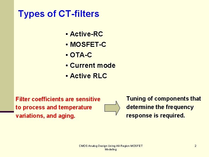
Types of CT-filters • Active-RC • MOSFET-C • OTA-C • Current mode • Active RLC Filter coefficients are sensitive to process and temperature variations, and aging. Tuning of components that determine the frequency response is required. CMOS Analog Design Using All-Region MOSFET Modeling 2

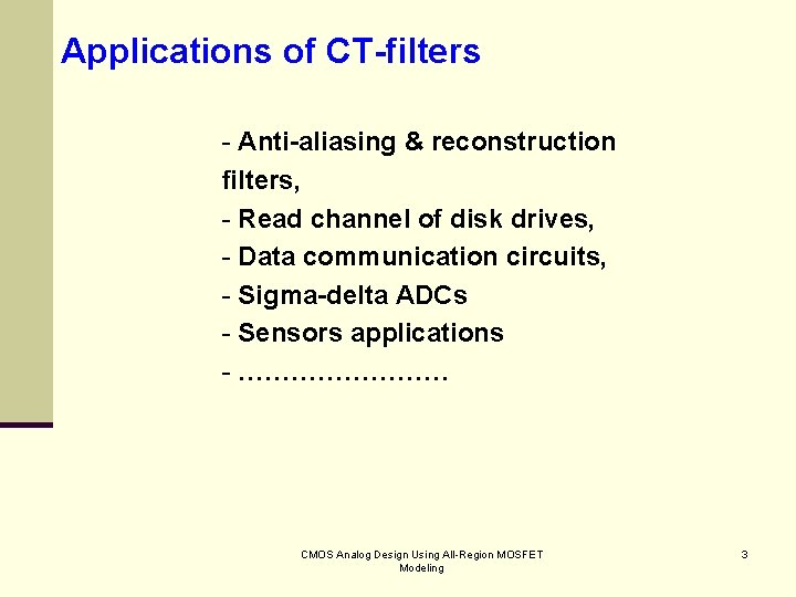
Applications of CT-filters - Anti-aliasing & reconstruction filters, - Read channel of disk drives, - Data communication circuits, - Sigma-delta ADCs - Sensors applications - ………… CMOS Analog Design Using All-Region MOSFET Modeling 3

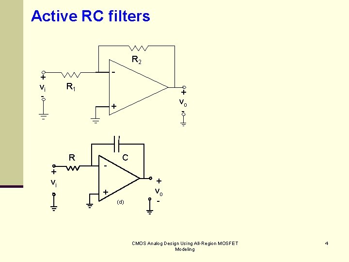
Active RC filters R 2 - + vi - R 1 + vo - + R + vi - - C + (d) + vo - CMOS Analog Design Using All-Region MOSFET Modeling 4

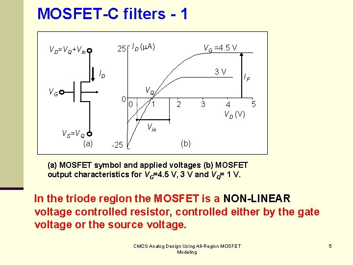
MOSFET-C filters - 1 25 ID ( A) VD=VQ+Vin VG =4. 5 V 3 V ID VG 0 VS=VQ (a) IF VQ 0 1 2 3 5 4 VD (V) Vin -25 (b) (a) MOSFET symbol and applied voltages (b) MOSFET output characteristics for VG=4. 5 V, 3 V and VQ= 1 V. In the triode region the MOSFET is a NON-LINEAR voltage controlled resistor, controlled either by the gate voltage or the source voltage. CMOS Analog Design Using All-Region MOSFET Modeling 5

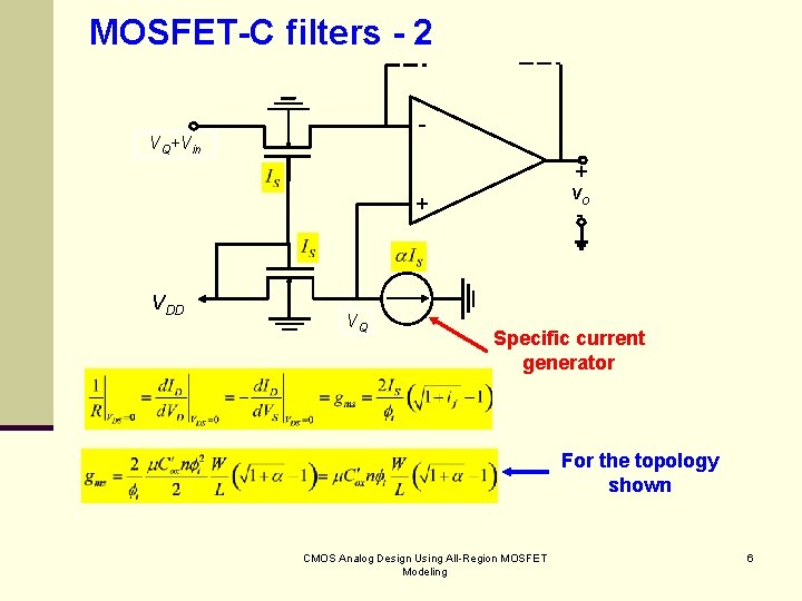
MOSFET-C filters - 2 - VQ+Vin + vo - + VDD VQ Specific current generator For the topology shown CMOS Analog Design Using All-Region MOSFET Modeling 6

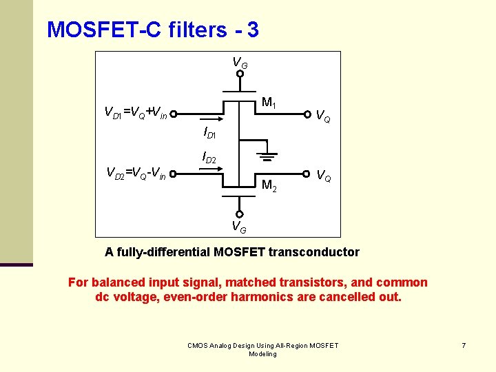
MOSFET-C filters - 3 VG M 1 VD 1=VQ+Vin VQ ID 1 ID 2 VD 2=VQ-Vin M 2 VQ VG A fully-differential MOSFET transconductor For balanced input signal, matched transistors, and common dc voltage, even-order harmonics are cancelled out. CMOS Analog Design Using All-Region MOSFET Modeling 7

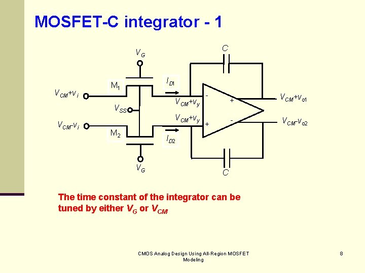
MOSFET-C integrator - 1 C VG VCM+vi ID 1 M 1 VCM+vy VSS VCM-vi VCM+vy M 2 + + VCM+vo 1 - VCM-vo 2 ID 2 VG C The time constant of the integrator can be tuned by either VG or VCM CMOS Analog Design Using All-Region MOSFET Modeling 8

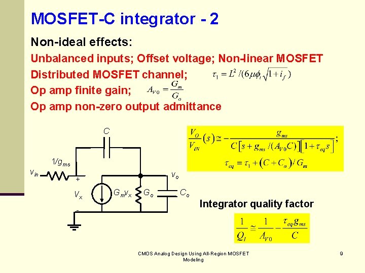
MOSFET-C integrator - 2 Non-ideal effects: Unbalanced inputs; Offset voltage; Non-linear MOSFET Distributed MOSFET channel; Op amp finite gain; Op amp non-zero output admittance C vin 1/gms vo + Vx - Gmvx Go Co Integrator quality factor CMOS Analog Design Using All-Region MOSFET Modeling 9

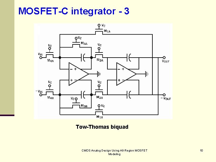
MOSFET-C integrator - 3 Tow-Thomas biquad CMOS Analog Design Using All-Region MOSFET Modeling 10

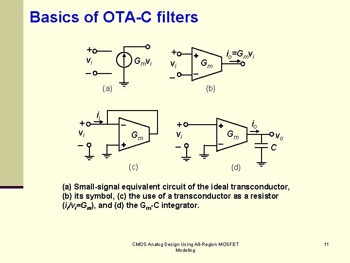
Basics of OTA-C filters + vi _ Gmvi + vi _ Gm (b) (a) ii io=Gmvi _ + Gm (c) + vi _ + _ Gm io vo C (d) (a) Small-signal equivalent circuit of the ideal transconductor, (b) its symbol, (c) the use of a transconductor as a resistor (ii/vi=Gm), and (d) the Gm-C integrator. CMOS Analog Design Using All-Region MOSFET Modeling 11

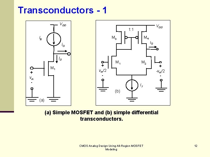
Transconductors - 1 VDD 1: 1 M 4 M 3 IB i. O ID M 1 + vin - + vin/2 - M 1 M 2 i. O + -vin/2 - IT (b) (a) Simple MOSFET and (b) simple differential transconductors. CMOS Analog Design Using All-Region MOSFET Modeling 12

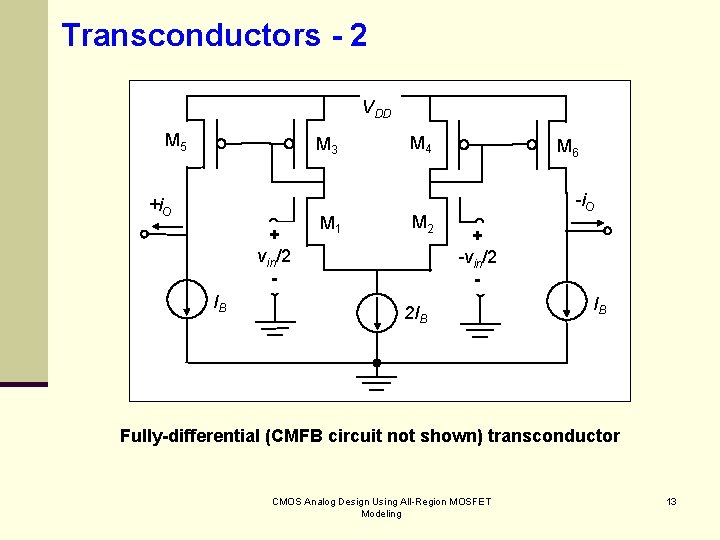
Transconductors - 2 VDD M 5 M 3 +i. O + vin/2 IB M 1 M 4 M 2 M 6 -i. O + -vin/2 - 2 IB IB Fully-differential (CMFB circuit not shown) transconductor CMOS Analog Design Using All-Region MOSFET Modeling 13

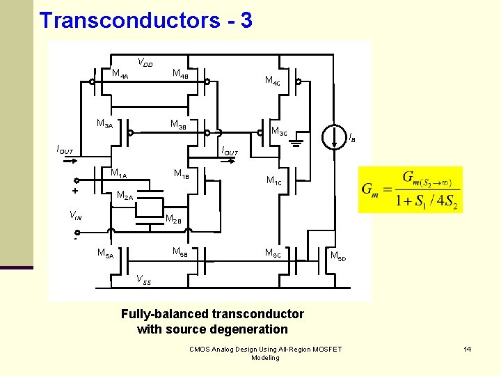
Transconductors - 3 M 4 A VDD M 3 A M 4 B M 4 C M 3 B M 3 C IOUT IB IOUT M 1 A + M 1 B M 1 C M 2 A VIN M 2 B M 5 A M 5 C M 5 D VSS Fully-balanced transconductor with source degeneration CMOS Analog Design Using All-Region MOSFET Modeling 14

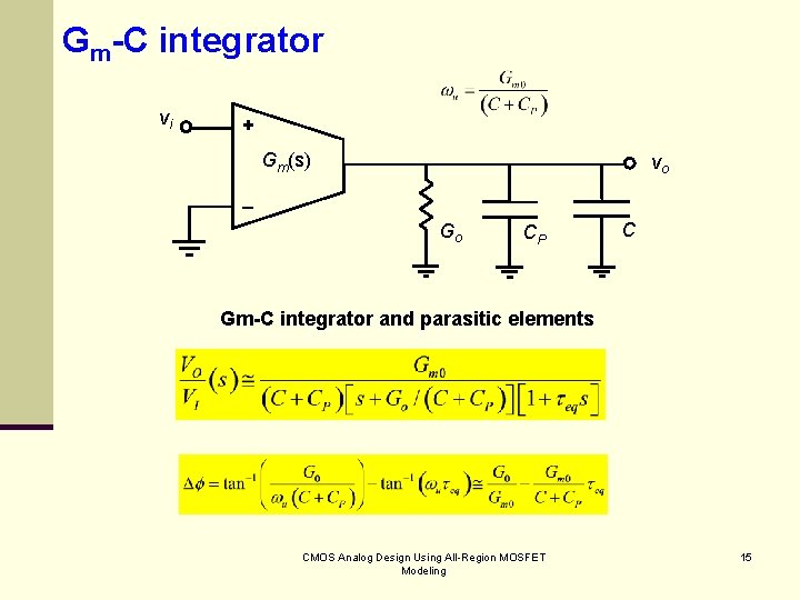
Gm-C integrator vi + Gm(s) vo _ Go CP C Gm-C integrator and parasitic elements CMOS Analog Design Using All-Region MOSFET Modeling 15

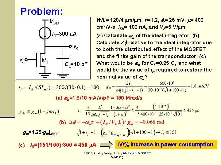
Problem: W/L= 120/4 m/ m, n=1. 2, t= 25 m. V, = 400 cm 2/V-s, ISH= 100 n. A, and VE=5 V/ m. VDD IB=300 A vo vi M 1 CL=10 p. F (a) Calculate u of the ideal integrator; (b) Calculate relative to the ideal integrator due to both the distributed effect of the MOSFET and the finite gain of the transconductor; (c) What would be u for CP=0. 25·CL and what would be the value of IB required to restore the nominal value of u? (a) u=1. 8/10 m. A/V/p. F = 180 Mrad/s (b) gm=1. 25·gm|if=100 (c) IB=(151/100)· 300 = 450 A 50% increase in power consumption CMOS Analog Design Using All-Region MOSFET Modeling

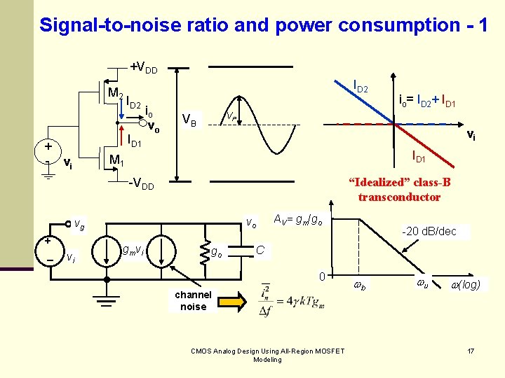
Signal-to-noise ratio and power consumption - 1 +VDD M 2 ID 1 + - vi ID 2 io vo VP VB vi ID 1 M 1 “Idealized” class-B transconductor -VDD vi AV= gm/go vo vg + gmvi io= ID 2+ ID 1 go -20 d. B/dec C 0 channel noise CMOS Analog Design Using All-Region MOSFET Modeling b u (log) 17

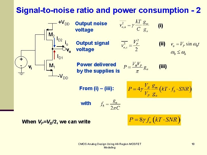
Signal-to-noise ratio and power consumption - 2 +VDD M 2 + - ID 2 ID 1 vi Output noise voltage io Output signal vo voltage M 1 -VDD Power delivered by the supplies is (i) (iii) From (i) – (iii): with When VP=VB/2, we can write CMOS Analog Design Using All-Region MOSFET Modeling 18

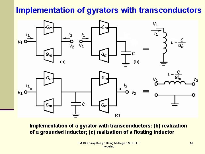
Implementation of gyrators with transconductors Implementation of a gyrator with transconductors; (b) realization of a grounded inductor; (c) realization of a floating inductor CMOS Analog Design Using All-Region MOSFET Modeling 19

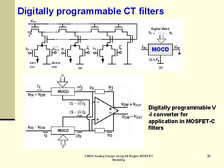
Digitally programmable CT filters MOCD Digitally programmable V -I converter for application in MOSFET-C filters CMOS Analog Design Using All-Region MOSFET Modeling 20

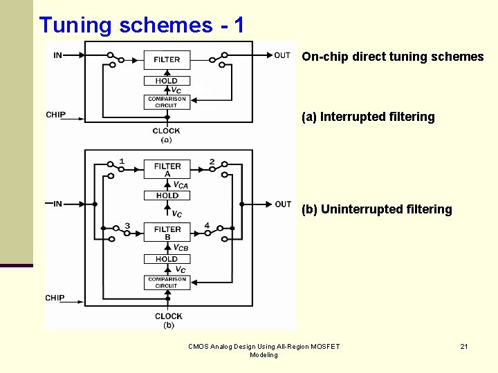
Tuning schemes - 1 On-chip direct tuning schemes (a) Interrupted filtering (b) Uninterrupted filtering CMOS Analog Design Using All-Region MOSFET Modeling 21

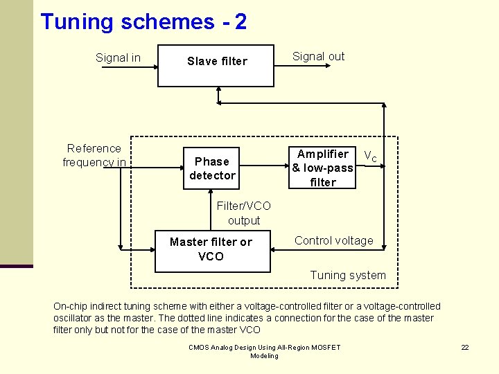
Tuning schemes - 2 Signal in Reference frequency in Slave filter Signal out Phase detector Amplifier VC & low-pass filter Filter/VCO output Master filter or VCO Control voltage Tuning system On-chip indirect tuning scheme with either a voltage-controlled filter or a voltage-controlled oscillator as the master. The dotted line indicates a connection for the case of the master filter only but not for the case of the master VCO CMOS Analog Design Using All-Region MOSFET Modeling 22