CMOS Analog Design Using AllRegion MOSFET Modeling Chapter

- Slides: 23

CMOS Analog Design Using All-Region MOSFET Modeling Chapter 10 Fundamentals of sampled-data circuits CMOS Analog Design Using All-Region MOSFET Modeling

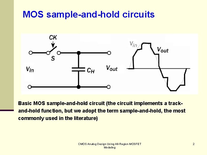
MOS sample-and-hold circuits Basic MOS sample-and-hold circuit (the circuit implements a trackand-hold function, but we adopt the term sample-and-hold, the most commonly used in the literature) CMOS Analog Design Using All-Region MOSFET Modeling 2

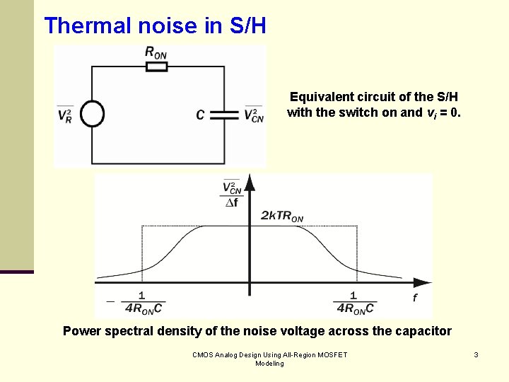
Thermal noise in S/H Equivalent circuit of the S/H with the switch on and vi = 0. Power spectral density of the noise voltage across the capacitor CMOS Analog Design Using All-Region MOSFET Modeling 3

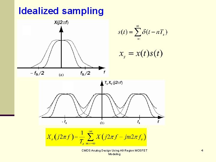
Idealized sampling CMOS Analog Design Using All-Region MOSFET Modeling 4

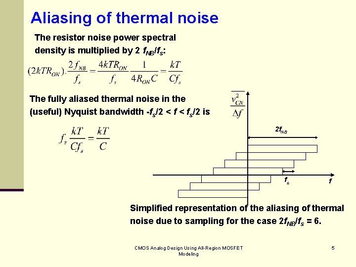
Aliasing of thermal noise The resistor noise power spectral density is multiplied by 2 f. NB/fs: The fully aliased thermal noise in the (useful) Nyquist bandwidth -fs/2 < fs/2 is 2 f. NB fs f Simplified representation of the aliasing of thermal noise due to sampling for the case 2 f. NB/fs = 6. CMOS Analog Design Using All-Region MOSFET Modeling 5

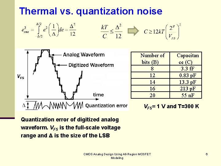
Thermal vs. quantization noise Number of bits (B) 8 12 14 16 20 Capacitan ce (C) 3. 3 f. F 0. 83 p. F 13. 3 p. F 213 p. F 55 n. F VFS= 1 V and T=300 K Quantization error of digitized analog waveform. VFS is the full-scale voltage range and Δ is the size of the LSB CMOS Analog Design Using All-Region MOSFET Modeling 6

Switch on-resistance 0 Vin Variation of the on-conductance of the n. MOS, p. MOS, and CMOS switches with the input voltage. Illustration of the distortion produced by the inputdependent delay of the MOS S/H in the tracking mode CMOS Analog Design Using All-Region MOSFET Modeling 7

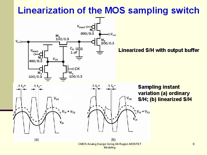
Linearization of the MOS sampling switch Linearized S/H with output buffer Sampling instant variation (a) ordinary S/H; (b) linearized S/H CMOS Analog Design Using All-Region MOSFET Modeling 8

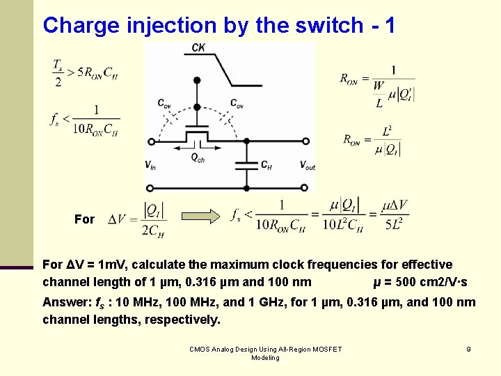
Charge injection by the switch - 1 For ΔV = 1 m. V, calculate the maximum clock frequencies for effective channel length of 1 µm, 0. 316 µm and 100 nm µ = 500 cm 2/V·s Answer: fs : 10 MHz, 100 MHz, and 1 GHz, for 1 µm, 0. 316 µm, and 100 nm channel lengths, respectively. CMOS Analog Design Using All-Region MOSFET Modeling 9

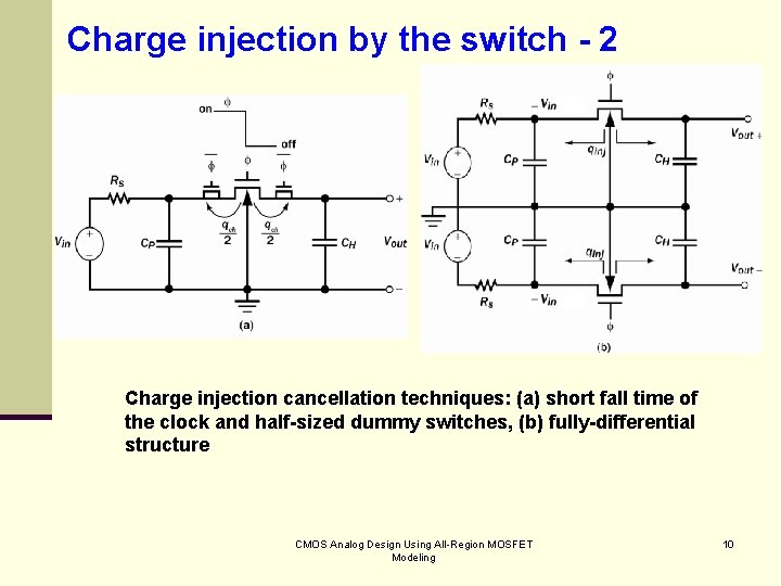
Charge injection by the switch - 2 Charge injection cancellation techniques: (a) short fall time of the clock and half-sized dummy switches, (b) fully-differential structure CMOS Analog Design Using All-Region MOSFET Modeling 10

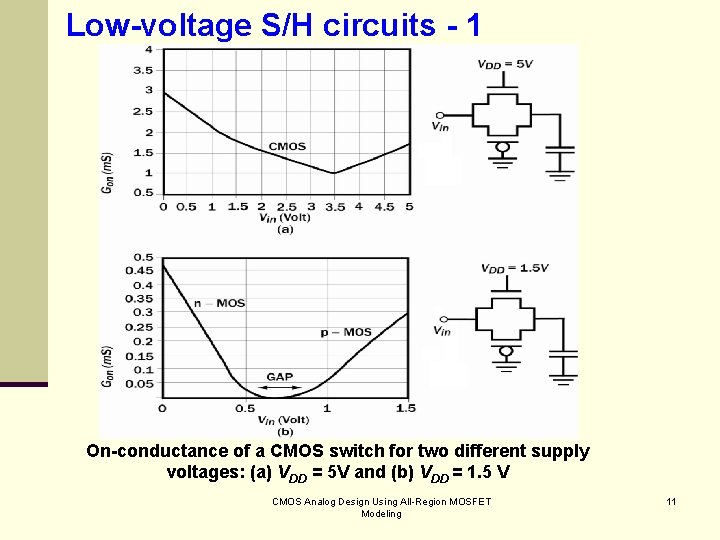
Low-voltage S/H circuits - 1 On-conductance of a CMOS switch for two different supply voltages: (a) VDD = 5 V and (b) VDD = 1. 5 V CMOS Analog Design Using All-Region MOSFET Modeling 11

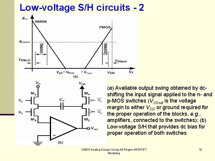
Low-voltage S/H circuits - 2 (a) Available output swing obtained by dcshifting the input signal applied to the n- and p-MOS switches (VDSsat is the voltage margin to either VDD or ground required for the properation of the blocks, e. g. , amplifiers, connected to the switches); (b) Low-voltage S/H that provides dc bias for properation of both switches CMOS Analog Design Using All-Region MOSFET Modeling 12

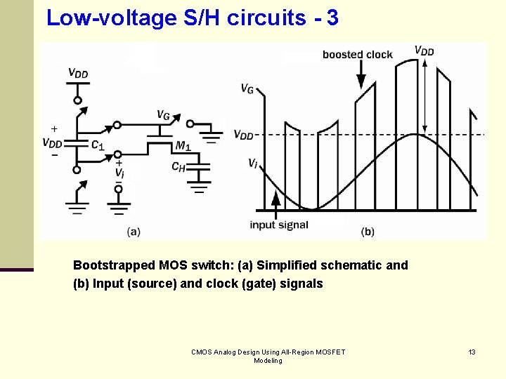
Low-voltage S/H circuits - 3 Bootstrapped MOS switch: (a) Simplified schematic and (b) Input (source) and clock (gate) signals CMOS Analog Design Using All-Region MOSFET Modeling 13

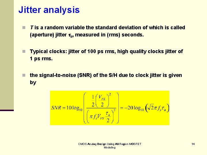
Jitter analysis n T is a random variable the standard deviation of which is called (aperture) jitter a, measured in (rms) seconds. n Typical clocks: jitter of 100 ps rms, high quality clocks jitter of 1 ps rms. n the signal-to-noise (SNR) of the S/H due to clock jitter is given by CMOS Analog Design Using All-Region All Region MOSFET Modeling 14

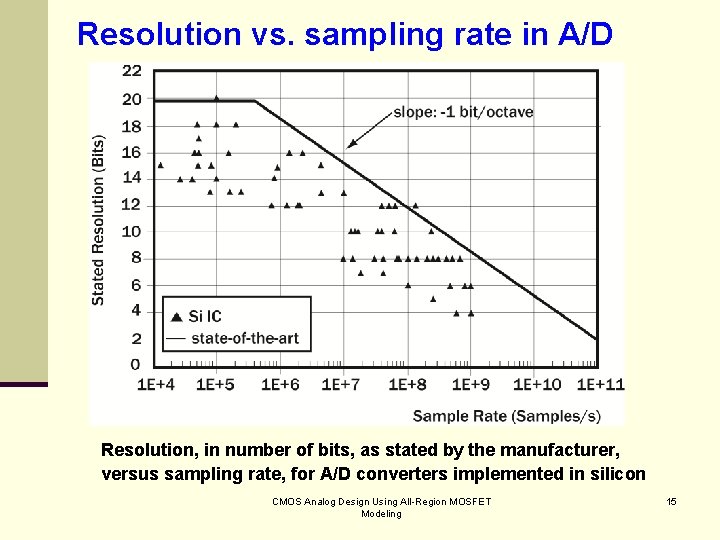
Resolution vs. sampling rate in A/D Resolution, in number of bits, as stated by the manufacturer, versus sampling rate, for A/D converters implemented in silicon CMOS Analog Design Using All-Region MOSFET Modeling 15

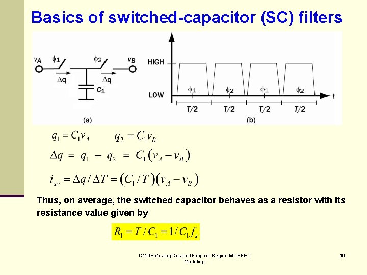
Basics of switched-capacitor (SC) filters Thus, on average, the switched capacitor behaves as a resistor with its resistance value given by CMOS Analog Design Using All-Region MOSFET Modeling 16

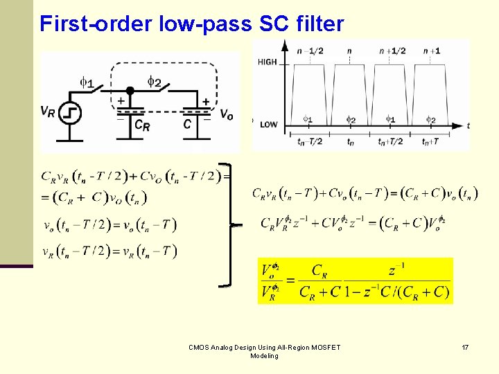
First-order low-pass SC filter CMOS Analog Design Using All-Region MOSFET Modeling 17

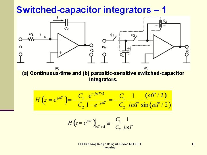
Switched-capacitor integrators – 1 (a) Continuous-time and (b) parasitic-sensitive switched-capacitor integrators. CMOS Analog Design Using All-Region MOSFET Modeling 18

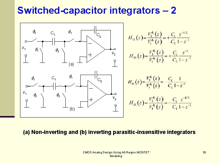
Switched-capacitor integrators – 2 2 v 1 1 1 C 2 2 v 2 (a) 1 v 1 2 1 C 1 2 C 2 v 2 (b) (a) Non-inverting and (b) inverting parasitic-insensitive integrators CMOS Analog Design Using All-Region MOSFET Modeling 19

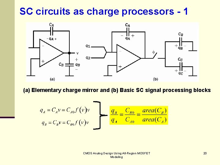
SC circuits as charge processors - 1 (a) Elementary charge mirror and (b) Basic SC signal processing blocks CMOS Analog Design Using All-Region MOSFET Modeling 20

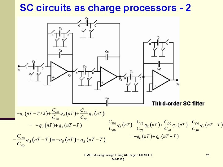
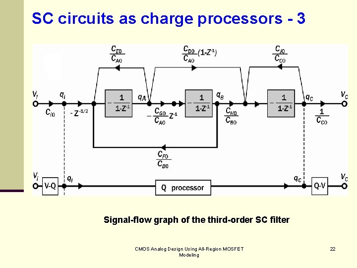
SC circuits as charge processors - 2 Third-order SC filter CMOS Analog Design Using All-Region MOSFET Modeling 21

SC circuits as charge processors - 3 Signal-flow graph of the third-order SC filter CMOS Analog Design Using All-Region MOSFET Modeling 22

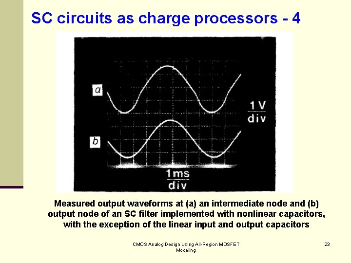
SC circuits as charge processors - 4 Measured output waveforms at (a) an intermediate node and (b) output node of an SC filter implemented with nonlinear capacitors, with the exception of the linear input and output capacitors CMOS Analog Design Using All-Region MOSFET Modeling 23