CMOS AMPLIFIERS Introduction to Op Amp Types of


=Iinj Ytot")
=Iinj Same")
 When w ∞, A(s)")

 Closed-loop zero: z 1 Feedback changed pole location, but does")


 Initially, as W 1 increased, GB")

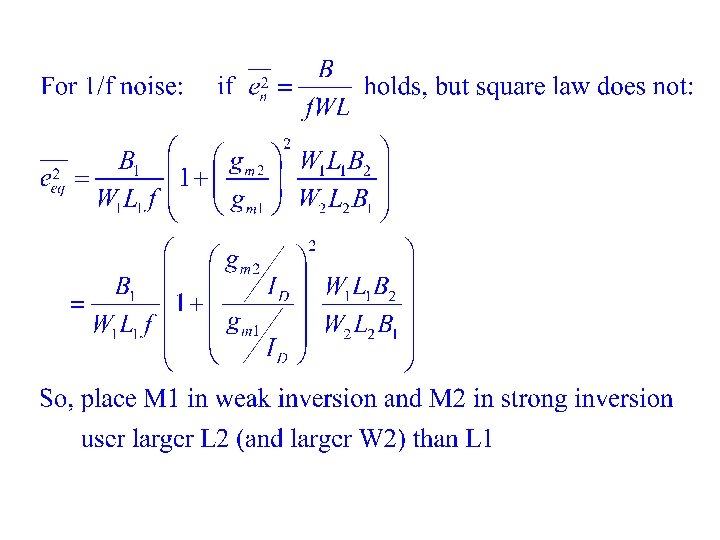
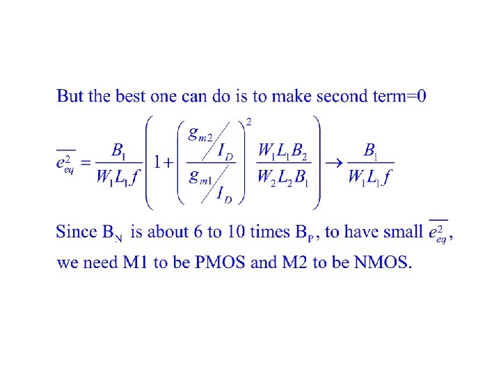
 L 2 >>L 1 2) en 1 small")

- Slides: 45
CMOS AMPLIFIERS • Introduction to Op Amp • Types of amplifiers – – Simple Inverting Amplifier Differential Amplifiers Cascode Amplifier Output Amplifiers • Components – – Current mirrors Current sources, current sinks Voltage and current references Switches, resistors, capacitors
Op Amp structure
Types of Amplifiers Common source, input pairs, are transconductance Most whole CMOS op amps are transconductance Common gate can be viewed as current amplifier Current mirrors are current amplifier Common drain or source follower is voltage amplifier Can cascade two or more basic one to get new types
Single transistor amplifiers, building blocks Rin = Rout =
Amplifier Notation
Analysis of amplifiers • DC analysis – Find DC operating points, i. e. , quiescent point, or Q point – Finding the quiescent voltages VXXQ’s at various nodes – Finding IXXQ’s through various branches • Large signal static analysis – Plot of output versus input (transfer curve) – Large signal gain – Output and input swing limits • Small signal static and AC analysis – DC gain A 0, AC gain A(s) – Input resistance/impedance, output resistance/impedance • Small signal dynamic analysis – Bandwidth, overshoot, settling – Noise – Power supply rejection • Large signal dynamic analysis – Slew rate – Nonlinearity
Simple Inverting Amplifiers
Common source with diode load VDD v. OUT |VTP| M 1/2 sat vod. P M 1 cutoff M 2 sat V vod. N N T V - GS M 1 tiode M 2 sat VTN ID = ½b. P(VDD-v. OUT -|VTP|)2(1+l. P(VDD-v. OUT)) = ½b. N(v. IN-VTN)2(1+l. Nv. OUT) v. IN
Large signal limits Absolute limits: None for v_in v_out: v_out at Vin=V DD to VDD-VTP To have all transistors in saturation: Vin range: Vout range:
Inverter with diode connection load Small Signal Characteristics
High gain inverters
Current source load or push-pull • Refer to book for large signal analysis • Must match quiescent currents in PMOS and NMOS transistors • Wider output swing, especially push-pull • Much higher gain (at DC), but much lower -3 d. B frequency (vs diode load) • About the same GB • Very power dependent
Small signal High gain! Especially at low power.
Dependence of Gain upon Bias Current ID ID Vg Vo + + Vo+D Vg
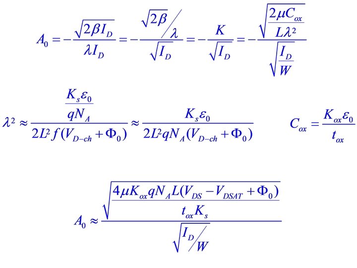
3 ways to increase A 0: larger L, sufficient VDS, and small current density. But: Larger L reduces f. T, slows down operation. VDS freedom is limited: in the 2 nd stage VDS range is larger but must meet Vo swing requirement; 1 st stage VDS range is quite small. Small current density also leads to slow operation.
Key to analysis by hand: • Use level 1 or 3 model equations • Use KCL/KVL
Transfer function of a system input u zeros poles System output y
For stability • All closed loop poles must have negative real parts – But open loop poles do not need to be stable – Feedback changes the location of the poles • Location of zeros cannot be changed by feedback – Right half plane zeros do not cause instability by themselves – But they have very negative impact on phase margin, making stabilization more difficult
Nodal analysis • Identify nontrivial nodes • Write a KCL at each node • Solve for TF from input to output
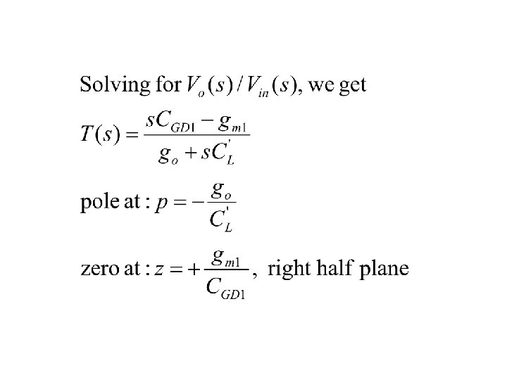
Frequency Response of CMOS Inverters Only one non trivial node KCL: Ytot. Vout(s)=Iinj Ytot =gds 1+gds 2+s. Cgd 1 +s. CBD 1+s. CL+s. CBD 2 +s. CGD 2 =go+s. CL’ Iinj=-gm 1 vin+s. CGD 1 vin
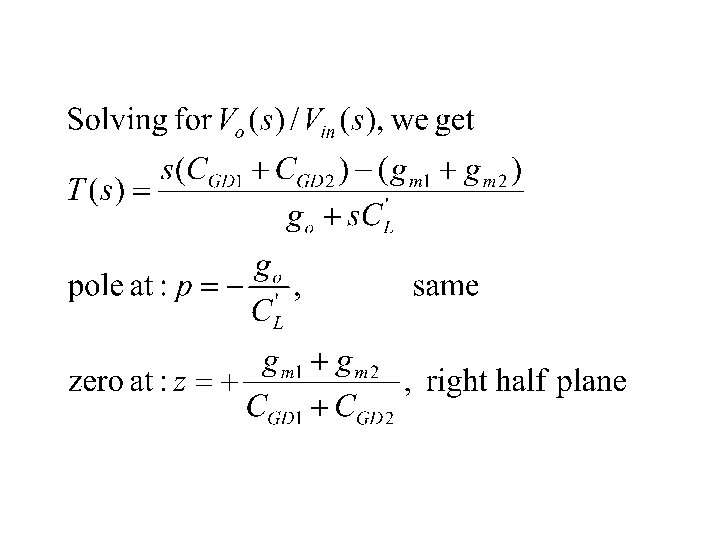
CMOS Inverters Let x=vin Still only one non trivial node KCL: Ytot. Vout(s)=Iinj Same Ytot =gds 1+gds 2+s. Cgd 1 +s. CBD 1+s. CL+s. CBD 2 +s. CGD 2 =go+s. CL’ But Iinj=-gm 1 vin+s. CGD 1 vin –gm 2 vin+s. CGD 2 vin
Input output transfer function When s=jw 0, A(0) When w ∞, A(s)
-3 d. B frequency of closed loop =b*GB |A 0 | =gm/go Acl=1/b 0 d. B |p 1|= g 0/CL’ Unity gain frequency =|A 0 p 1| =GB =gm/CL’ |z 1| =gm/Cgd =GB*CL’/Cgd
Unity gain feedback A(s) Closed-loop zero: z 1 Feedback changed pole location, but does not change zero location.
If a step input is given, the output response is By the final value theorem: By the initial value theorem:
Right half plane zero causes initial reverse transient, whose size depends on main pole/zero ratio. -1 Final settling determined by A 0 need high gain Settling speed determined by A 0 p 1=GB=UGF, need high gain bandwidth product
Gain bandwidth product C’L = Ctotal = CGD 1+ CGD 2+ CBD 1+ CBD 2+ CL When CL ≈ C’L, W↑ GB↑, but it saturates, when
More on gain bandwidth product
For small CL GB 0 W 1
At max GB sizing • Use small L • Use NMOS for larger m • Large Cox: thin oxide and high K • Small gate drain overlap DL, small side wall capacitance density • Sufficient current density
Max GB and slew rate
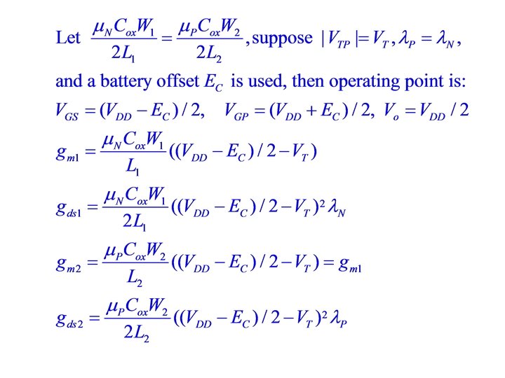
Note: If VEB 1 and VEB 2 are fixed, W 1/L 1 and W 2/L 2 must be adjusted proportionally, and they are proportional to DC power.
Therefore: P is proportional to W 1, W 2 CL constant, but C(W 1, W 2) proportional to W 1, W 2 When C(W 1, W 2) << CL, GB proportional to P When C(W 1, W 2) CL or >CL, GB saturates
GB Linear increase region P
For given current or power (current source load) Initially, as W 1 increased, GB increases But GB will reach a max, and then drop as W 1 increases
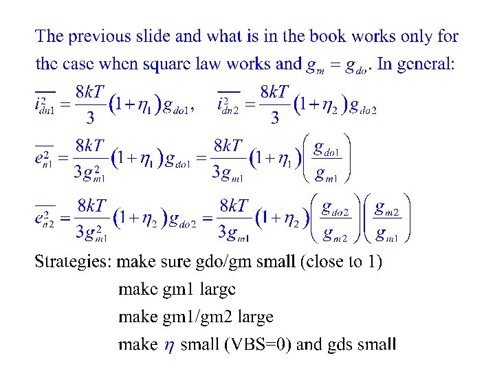
NOISE IN MOS INVERTERS
To minimize: 1) L 2 >>L 1 2) en 1 small
For thermal noise