Clocking and Dynamic Discipline 1 FlipFlop timing 2
- Slides: 15

Clocking and Dynamic Discipline 1. Flip-Flop timing 2. Dynamic Discipline Handouts: Lecture Slides 1

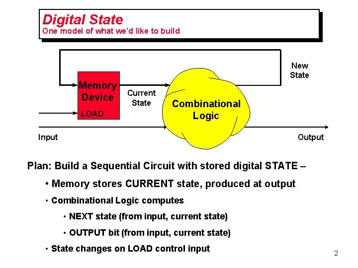
Digital State One model of what we’d like to build New State Memory Device LOAD Current State Combinational Logic Input Output Plan: Build a Sequential Circuit with stored digital STATE – • Memory stores CURRENT state, produced at output • Combinational Logic computes • NEXT state (from input, current state) • OUTPUT bit (from input, current state) • State changes on LOAD control input 2

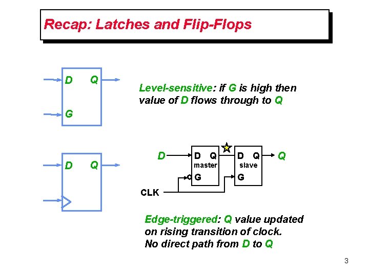
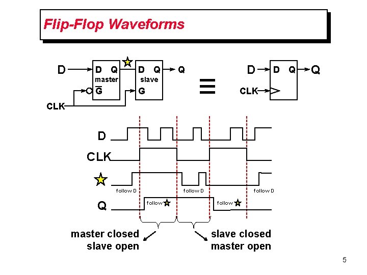
Recap: Latches and Flip-Flops D Q Level-sensitive: if G is high then value of D flows through to Q G D Q D Q master slave G G Q CLK Edge-triggered: Q value updated on rising transition of clock. No direct path from D to Q 3

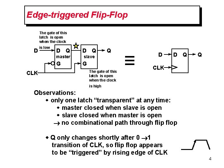
Edge-triggered Flip-Flop The gate of this latch is open when the clock D CLK is low D Q master slave G G Q The gate of this latch is open when the clock D D Q Q CLK is high Observations: w only one latch “transparent” at any time: w master closed when slave is open w slave closed when master is open no combinational path through flip flop w Q only changes shortly after 0 1 transition of CLK, so flip flop appears to be “triggered” by rising edge of CLK 4

Flip-Flop Waveforms D D Q master slave G G D Q Q CLK D CLK follow D Q master closed slave open follow D follow slave closed master open 5

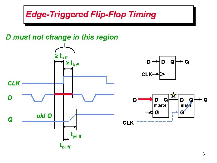
Edge-Triggered Flip-Flop Timing D must not change in this region ³ ts ff ³ th ff D D Q Q CLK D Q D old Q D Q master slave G G Q CLK tpd ff tcd ff 6

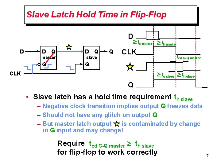
Slave Latch Hold Time in Flip-Flop D ³ ts master ³ th master D D Q master slave G G Q CLK tcd G-Q master ³ ts slave ³ th slave CLK Q • Slave latch has a hold time requirement th slave – Negative clock transition implies output Q freezes data – Should not have any glitch on output Q – But master latch output is contaminated by change in G input and may change! Require tcd G-Q master ³ th slave for flip-flop to work correctly 7

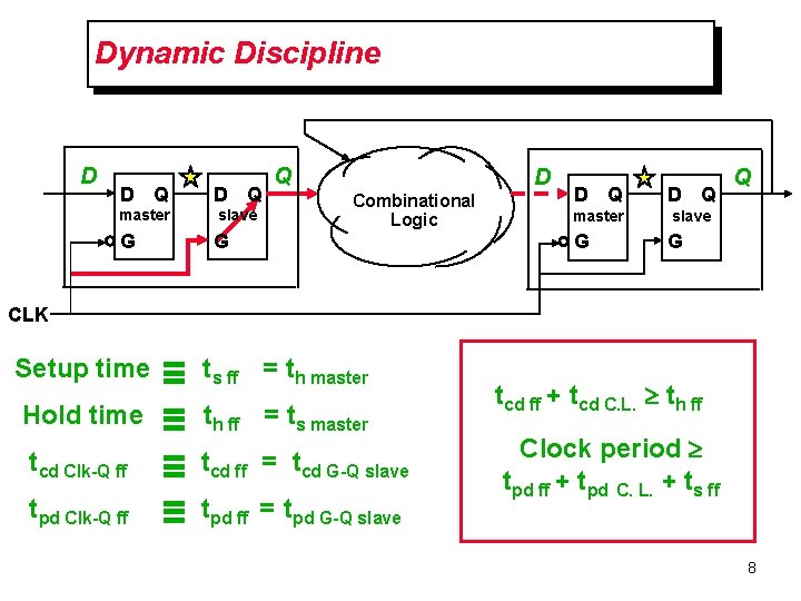
Dynamic Discipline D D Q master slave G G Q D Combinational Logic D Q master slave G G Q CLK Setup time ts ff = th master Hold time th ff = ts master tcd Clk-Q ff tcd ff = tcd G-Q slave tpd Clk-Q ff tpd ff = tpd G-Q slave tcd ff + tcd C. L. ³ th ff Clock period ³ tpd ff + tpd C. L. + ts ff 8

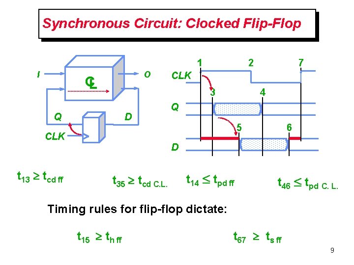
Synchronous Circuit: Clocked Flip-Flop 1 I O CL D CLK 7 CLK 3 Q t 13 ³ tcd ff 2 4 Q 5 6 D t 35 ³ tcd C. L. t 14 £ tpd ff t 46 £ tpd C. L. Timing rules for flip-flop dictate: t 15 ³ th ff t 67 ³ ts ff 9

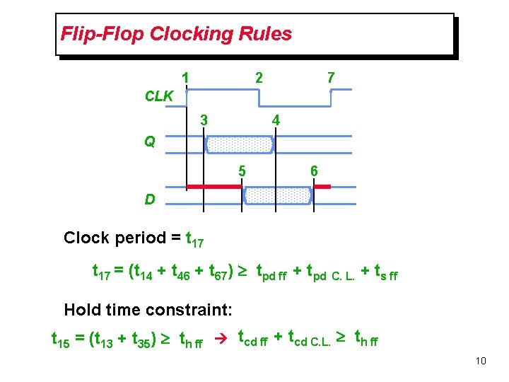
Flip-Flop Clocking Rules 1 2 7 CLK 3 4 Q 5 6 D Clock period = t 17 = (t 14 + t 46 + t 67) ³ tpd ff + tpd C. L. + ts ff Hold time constraint: t 15 = (t 13 + t 35) ³ th ff tcd ff + tcd C. L. ³ th ff 10

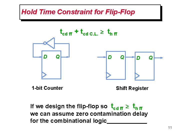
Hold Time Constraint for Flip-Flop tcd ff + tcd C. L. ³ th ff D Q 1 -bit Counter D Q Shift Register If we design the flip-flop so tcd ff ³ th ff we can assume zero contamination delay for the combinational logic 11

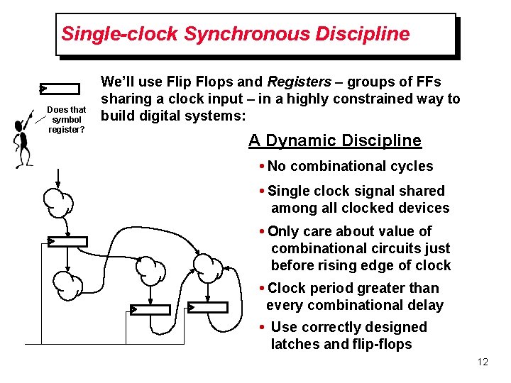
Single-clock Synchronous Discipline Does that symbol register? We’ll use Flip Flops and Registers – groups of FFs sharing a clock input – in a highly constrained way to build digital systems: A Dynamic Discipline • No combinational cycles • Single clock signal shared among all clocked devices • Only care about value of combinational circuits just before rising edge of clock • Clock period greater than every combinational delay • Use correctly designed latches and flip-flops 12

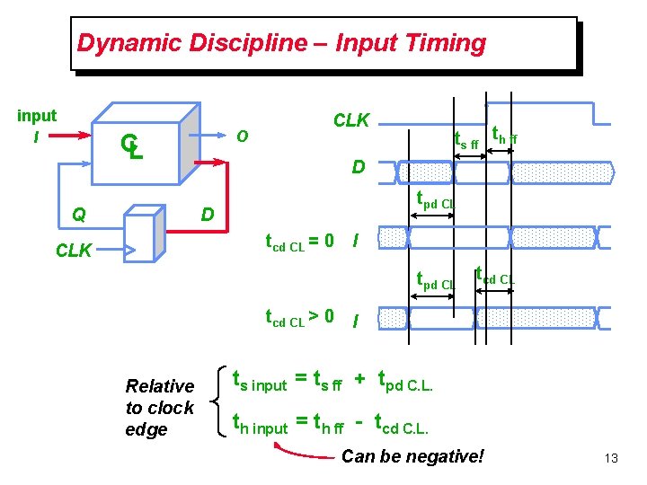
Dynamic Discipline – Input Timing input I O CL Q CLK D tpd CL D tcd CL = 0 CLK ts ff th ff I tpd CL tcd CL > 0 Relative to clock edge tcd CL I ts input = ts ff + tpd C. L. th input = th ff - tcd C. L. Can be negative! 13

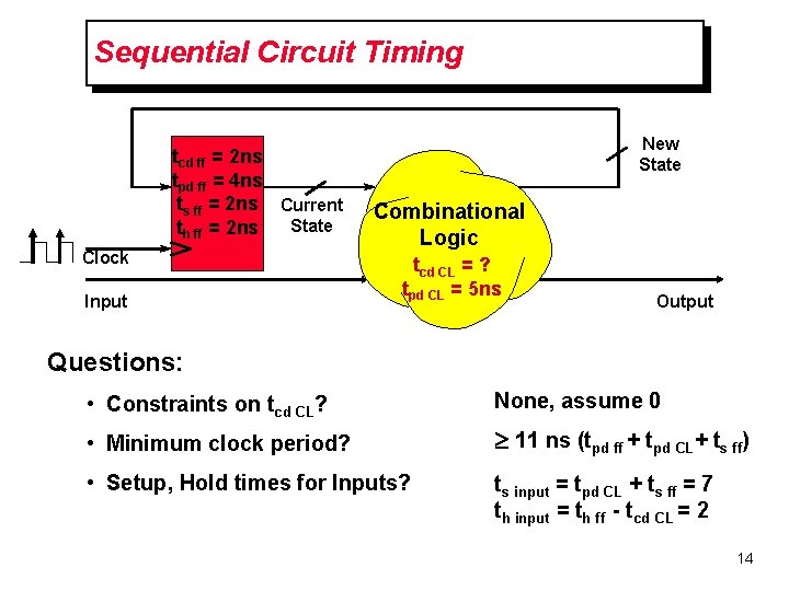
Sequential Circuit Timing tcd ff = 2 ns tpd ff = 4 ns ts ff = 2 ns Current State th ff = 2 ns Clock Input New State Combinational Logic tcd CL = ? tpd CL = 5 ns Output Questions: • Constraints on tcd CL? None, assume 0 • Minimum clock period? ³ 11 ns (tpd ff + tpd CL+ ts ff) • Setup, Hold times for Inputs? ts input = tpd CL + ts ff = 7 th input = th ff - tcd CL = 2 14

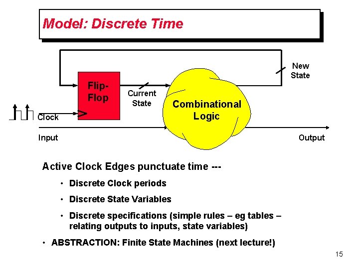
Model: Discrete Time New State Flip. Flop Current State Clock Combinational Logic Input Output Active Clock Edges punctuate time -- • Discrete Clock periods • Discrete State Variables • Discrete specifications (simple rules – eg tables – relating outputs to inputs, state variables) • ABSTRACTION: Finite State Machines (next lecture!) 15