
Clic Pix ideas and a first specification draft

- Slides: 13
Clic. Pix ideas and a first specification draft P. Valerio
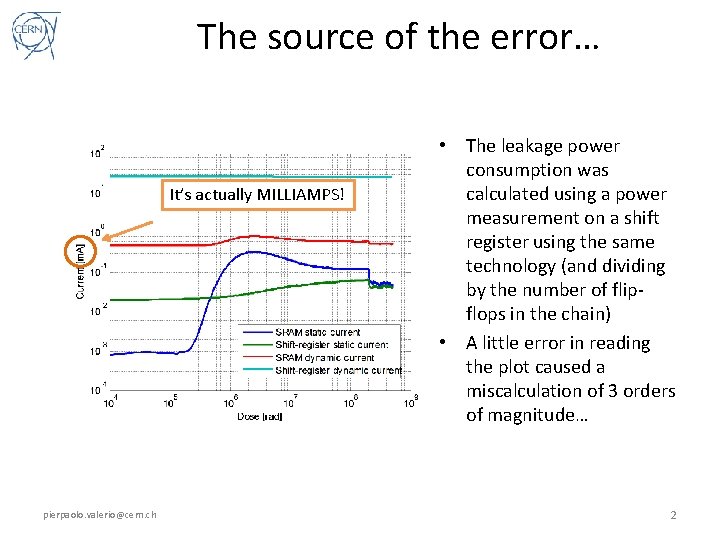
The source of the error… It’s actually MILLIAMPS! pierpaolo. valerio@cern. ch • The leakage power consumption was calculated using a power measurement on a shift register using the same technology (and dividing by the number of flipflops in the chain) • A little error in reading the plot caused a miscalculation of 3 orders of magnitude… 2
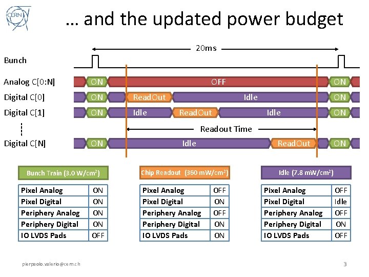
… and the updated power budget 20 ms Bunch OFF Sleep Analog C[0: N] ON Digital C[0] Sleep ON Read. Out Digital C[1] Sleep ON Idle ON ON Idle Read. Out ON Readout Time Digital C[N]Sleep ON Bunch Train (3. 0 W/cm 2) Pixel Analog Pixel Digital Periphery Analog Periphery Digital IO LVDS Pads pierpaolo. valerio@cern. ch ON ON OFF Read. Out Idle Chip Readout (360 m. W/cm 2) Pixel Analog Pixel Digital Periphery Analog Periphery Digital IO LVDS Pads OFF ON ON ON Idle (7. 8 m. W/cm 2) Pixel Analog Pixel Digital Periphery Analog Periphery Digital IO LVDS Pads OFF Idle OFF ON OFF 3
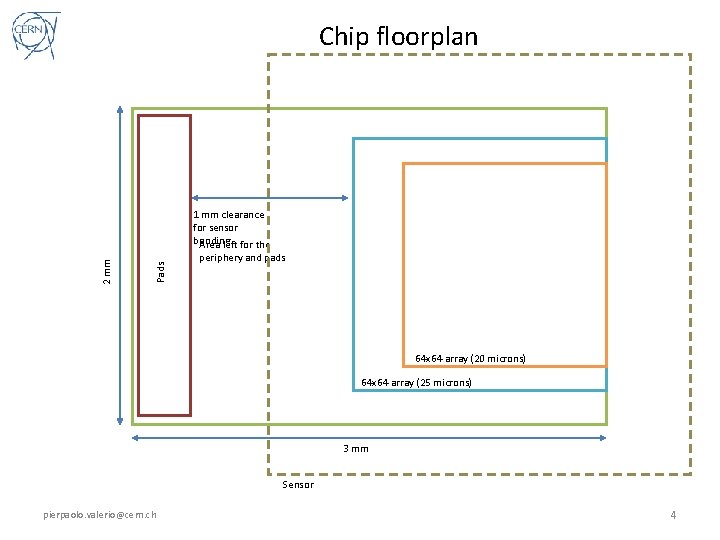
Chip floorplan Pads 2 mm 1 mm clearance for sensor bonding Area left for the periphery and pads 64 x 64 array (20 microns) 64 x 64 array (25 microns) Die area 3 mm Sensor pierpaolo. valerio@cern. ch 4
Sensor bonding • The chip will be functionally complete and it will be usable as a tracking detector (although it will have a smaller size and it will lack some automatic controls for debug purposes) • Testing the demonstrator in a beam or with a radioactive source would be ideal to fully test its performances and characterize it • In order to acquire data from a source, a sensor needs to be bonded to the chip. There are some problems in doing it: – The foundry will not give us any full wafer as the project will be implemented in a MPW – The pitch of the bonding is very small. Advanced technologies (copper pillars, indium bumps) will be needed – The pitch can be relaxed if we decide to bond only one every four pixels pierpaolo. valerio@cern. ch 5
Pixel logic • Each pixel includes simultaneous 4 -bits TOA and 4 -bits TOT measurements using a reference 100 MHz clock • The clock is distributed along each column exploiting the delays of buffers to give each pixel an “incoherent” clock signal, in order to simplify the clock distribution tree and to avoid a synchronous switch of every pixel in the matrix (which would affect the stability of the power supply) • The readout is on a per-column basis, distributing the full 320 MHz clock (for a DDR bandwidth of 640 Mbps) • A compression logic allows skipping pixels which were not hit during the acquisition. A cluster-based compression is being evaluated • Power saving techniques include clock gating when the pixel is not being read out and power gating (with an external signal) for the analog part when the chip is not acquiring data pierpaolo. valerio@cern. ch 6
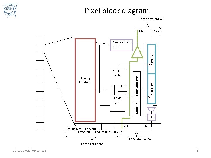
Pixel block diagram To the pixel above Clk Compression logic 4 bits tuning DAC Analog Frontend Clock divider Mask, TP Enable logic 4 bits TOA 4 bits TOT Disc_out Data HF Analog_bias Readout Poweroff Load_conf Shutter Clk Data To the pixel below To the periphery pierpaolo. valerio@cern. ch 7
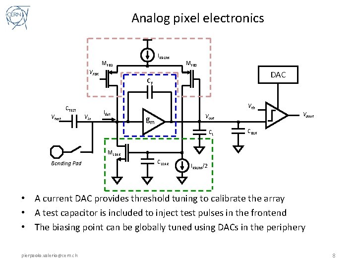
Analog pixel electronics IKRUM MFB 2 MFB 1 VFBK DAC CF CTEST Vtest Vin Idet Vth Vdout Vout gm CL CBUF MLEAK Bonding Pad CLEAK IKRUM/2 • A current DAC provides threshold tuning to calibrate the array • A test capacitor is included to inject test pulses in the frontend • The biasing point can be globally tuned using DACs in the periphery pierpaolo. valerio@cern. ch 8
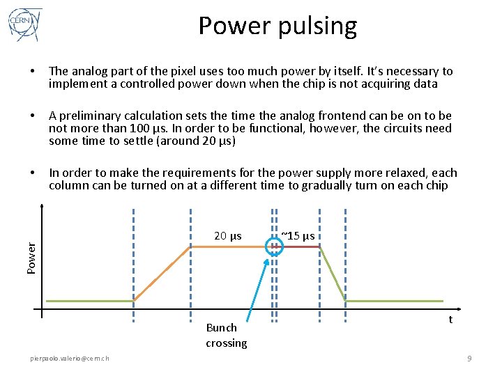
Power pulsing The analog part of the pixel uses too much power by itself. It’s necessary to implement a controlled power down when the chip is not acquiring data • A preliminary calculation sets the time the analog frontend can be on to be not more than 100 μs. In order to be functional, however, the circuits need some time to settle (around 20 μs) • In order to make the requirements for the power supply more relaxed, each column can be turned on at a different time to gradually turn on each chip Power • 20 μs Bunch crossing pierpaolo. valerio@cern. ch ~15 μs t 9
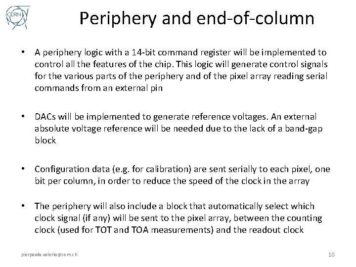
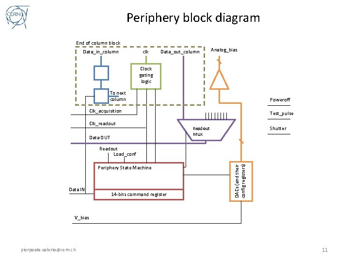
Periphery and end-of-column • A periphery logic with a 14 -bit command register will be implemented to control all the features of the chip. This logic will generate control signals for the various parts of the periphery and of the pixel array reading serial commands from an external pin • DACs will be implemented to generate reference voltages. An external absolute voltage reference will be needed due to the lack of a band-gap block • Configuration data (e. g. for calibration) are sent serially to each pixel, one bit per column, in order to reduce the speed of the clock in the array • The periphery will also include a block that automatically select which clock signal (if any) will be sent to the pixel array, between the counting clock (used for TOT and TOA measurements) and the readout clock pierpaolo. valerio@cern. ch 10
Periphery block diagram End of column block Data_in_column clk Data_out_column Analog_bias Clock gating logic To next column Poweroff Clk_acquisition Clk_readout Data OUT Test_pulse Shutter Readout MUX Periphery State Machine Data IN 14 -bits command register DACs (and their config registers) Readout Load_conf V_bias pierpaolo. valerio@cern. ch 11
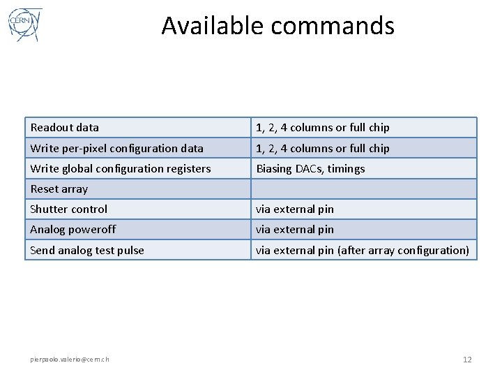
Available commands Readout data 1, 2, 4 columns or full chip Write per-pixel configuration data 1, 2, 4 columns or full chip Write global configuration registers Biasing DACs, timings Reset array Shutter control via external pin Analog poweroff via external pin Send analog test pulse via external pin (after array configuration) pierpaolo. valerio@cern. ch 12
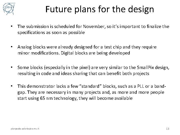
Future plans for the design • The submission is scheduled for November, so it’s important to finalize the specifications as soon as possible • Analog blocks were already designed for a test chip and they require minor modifications. Digital blocks are being developed • Some blocks (especially in the pixel) are very similar to the Small. Pix design, resulting in code and ideas sharing that can benefit both projects • This demonstrator lacks a few “standard” blocks, such as a PLL or a bandgap. They are necessary in many projects and, as more and more people start using 65 nm technology, they will become available pierpaolo. valerio@cern. ch 13