CLASSIFICATION OF SOLIDS INTERMS OF FORBIDDEN ENERGY GAP

CLASSIFICATION OF SOLIDS INTERMS OF FORBIDDEN ENERGY GAP

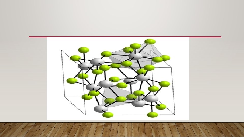
SEMICONDUCTING MATERIAL

BAND GAP & BAND ENERGY

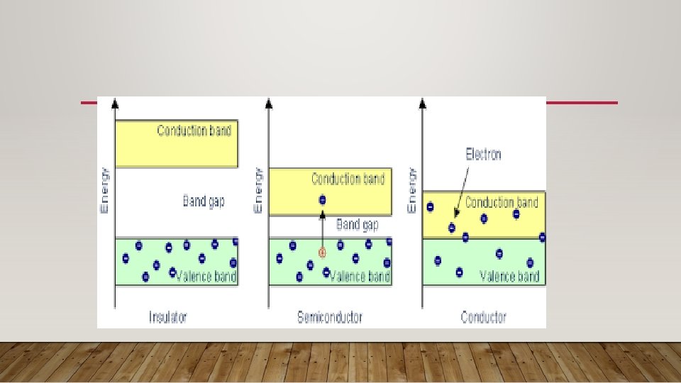
INTRODUCTION TO BAND GAP & BAND ENERGY • In solid-state physics, a band gap, also called an energy gap, is an energy range in a solid where no electronic states can exist. In graphs of the electronic band structure of solids, the band gap generally refers to the energy difference (in electron volts) between the top of the valence band the bottom of the conduction band in insulators and semiconductors. It is the energy required to promote a valence electron bound to an atom to become a conduction electron, which is free to move within the crystal lattice and serve as a charge carrier to conduct electric current.

INTRINSIC SEMICONDUCTORS BAND GAP • • The conductivity of intrinsic semiconductors is strongly dependent on the band gap. The only available charge carriers for conduction are the electrons that have enough thermal energy to be excited across the band gap and the electron holes that are left off when such an excitation occurs. • Band-gap engineering is the process of controlling or altering the band gap of a material by controlling the composition of certain semiconductor alloys, such as Ga. Al. As, In. Ga. As, and In. Al. As. It is also possible to construct layered materials with alternating compositions by techniques like molecular-beam epitaxy.

FERMI ENERGY LEVEL This Photo by Unknown Author is licensed under CC BY-SA

• Every solid has its own characteristic energy-band structure. This variation in band structure is responsible for the wide range of electrical characteristics observed in various materials. In semiconductors and insulators, electrons are confined to a number of bands of energy, and forbidden from other regions. The term "band gap" refers to the energy difference between the top of the valence band the bottom of the conduction band. Electrons are able to jump from one band to another. However, in order for an electron to jump from a valence band to a conduction band, it requires a specific minimum amount of energy for the transition. The required energy differs with different materials. Electrons can gain enough energy to jump to the conduction band by absorbing either a phonon (heat) or a photon (light).

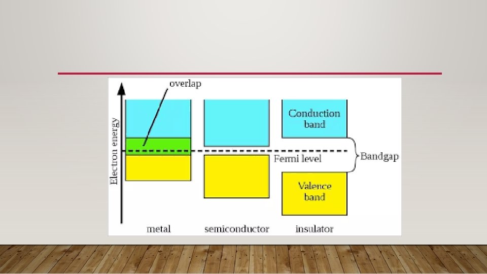
• A semiconductor is a material with an intermediate-sized but non-zero band gap that behaves as an insulator at absolute zero but allows thermal excitation of electrons into its conduction band at temperatures that are below its melting point. In contrast, a material with a large band gap is an insulator. In conductors, the valence and conduction bands may overlap, so they may not have a band gap.

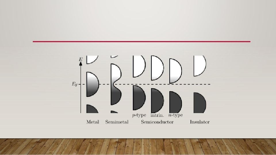
BAND GAP Based on the band structures, materials have either direct band gap or indirect band gap. If the momentum of the lowest energy state in the conduction band the highest energy state of the valence band of a material are the same, the material has a direct bandgap. If they are not the same, then the material has an indirect band gap. For materials with a direct band gap, valence electrons can be directly excited into the conduction band by a photon whose energy is larger than the bandgap. In contrast, for materials with an indirect band gap, a photon and phonon must both be involved in a transition from the valence band top to the conduction band bottom. Therefore, direct bandgap materials tend to have stronger light emission and absorption properties. Other things equal, direct bandgap materials tend to be better for photovoltaics (PVs), light-emitting diodes (LEDs), and laser diodes; however, indirect bandgap materials are frequently used in PVs and LEDs when the materials have other favorable properties.

• Silicon, germanium and graphite are some examples of semiconductors. In semiconductors, the forbidden gap between valence band conduction band is very small. It has a forbidden gap of about 1 electron volt (e. V). . This shows that electrical conductivity of the semiconductor increases with increase in temperature.

CLASSIFICATION OF ENERGY BANDS • Valence Band • The electrons in the outermost shell are known as valence electrons. These valence electrons contain a series of energy levels and form an energy band known as valence band. The valence band has the highest occupied energy.

CONDUCTION BAND • The valence electrons are not tightly held to the nucleus due to which a few of these valence electrons leave the outermost orbit even at room temperature and become free electrons. The free electrons conduct current in conductors and are therefore known as conduction electrons. The conduction band is one that contains conduction electrons and has the lowest occupied energy levels.

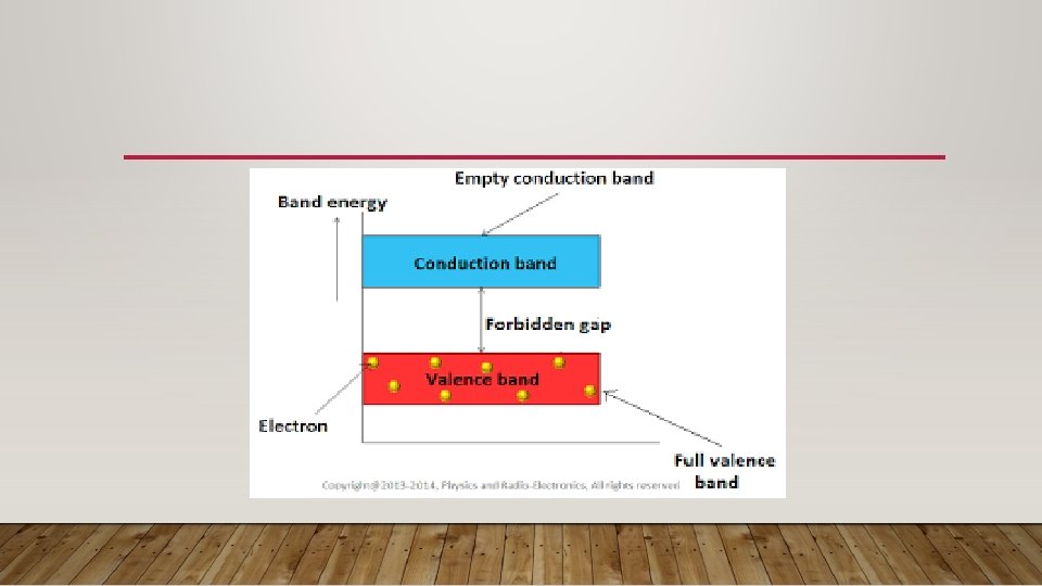
FORBIDDEN ENERGY GAP • The gap between the valence band the conduction band is referred to as forbidden gap. As the name suggests, the forbidden gap doesn’t have any energy and no electrons stay in this band. If the forbidden energy gap is greater, then the valence band electrons are tightly bound or firmly attached to the nucleus. We require some amount of external energy that is equal to the forbidden energy gap. • The figure below shows the conduction band, valence band the forbidden energy gap.

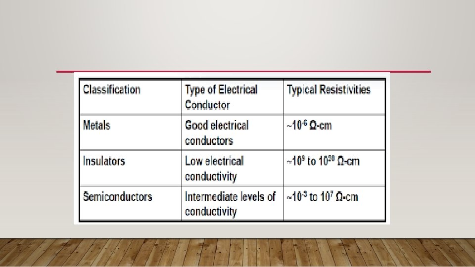
BAND GAP OF INSULATORS , SEMICONDUCTORS, AND CONDUCTORS

CONDUCTORS • Gold, Aluminium, Silver, Copper, all these metals allow an electric current to flow through them. • There is no forbidden gap between the valence band conduction band which results in the overlapping of both the bands. The number of free electrons available at room temperature is large.

INSULATORS • Glass and wood are examples of the insulator. These substances do not allow electricity to pass through them. They have high resistivity and very low conductivity. • The energy gap in the insulator is very high up to 7 e. V. The material cannot conduct because the movement of the electrons from the valence band to the conduction band is not possible.

SEMICONDUCTORS • Germanium and Silicon are the most preferable material whose electrical properties lie in between semiconductors and insulators. The energy band diagram of semiconductor is shown where the conduction band is empty and the valence band is completely filled but the forbidden gap between the two bands is very small that is about 1 e. V. For Germanium, the forbidden gap is 0. 72 e. V and for Silicon, it is 1. 1 e. V. Thus, semiconductor requires small conductivity.

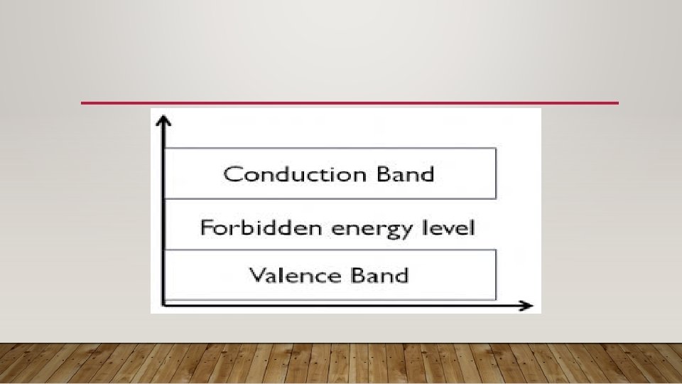
ENERGY BAND THEORY • According to Bohr’s theory, every shell of an atom contains a discrete amount of energy at different levels. Energy band theory explains the interaction of electrons between the outermost shell and the innermost shell. Based on the energy band theory, there are three different energy bands: 1. Valence band 2. Forbidden energy gap 3. Conduction band

WHAT IS BAND THEORY OF SOLIDS • This theory explains the quantum state that an electron takes inside metal solid. Every molecule comprises various discrete energy levels. The way electrons behave inside a molecule is well explained through this theory. • In atoms, electrons are filled in respective energy orbits following Pauli’s exclusion principle. • In molecules, Two atomic orbitals combine to form a molecular orbit with two distinct energy levels. • In solids, 1023 stacked up lines confined in a tiny space would look like a band. Thereby forming an energy continuum called energy bands. • This theory helps to visualize the difference between conductor, semiconductor, and an insulator by plotting available energies for an electron in a material.

ENERGY BANDS wn Author is licensed under

ENERGY BANDS This Photo by Unknown Author is licensed under CC BY-SA

- Slides: 29