Class 1 Class 2 Class 3 Class 4


 부품 Pin의 Pitch에 따라 Land Size를 구하며 특히 부품 Catalog를 참조할")
 4층 2층")
 형 명 (Inch) 1005 1608 2012 3216")
 D 55 E 55 F 60 H 63")
 SOP(Small Outline Package) TSOP(Thin Small Outline")
 QFJ(Quad Flat J-lead Package) LCC(Leadless Chip")
 ZIP(Zig-zag Inline Package) DIP(Dual Inline Package) PGA(Pin")


- Slides: 32
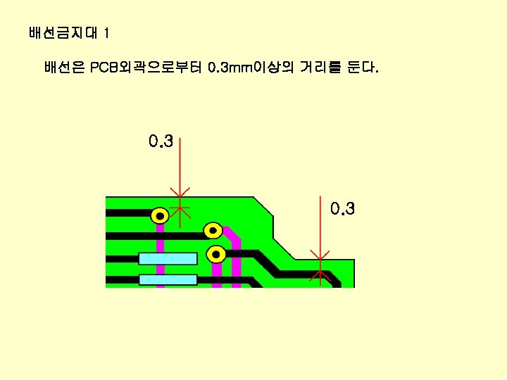
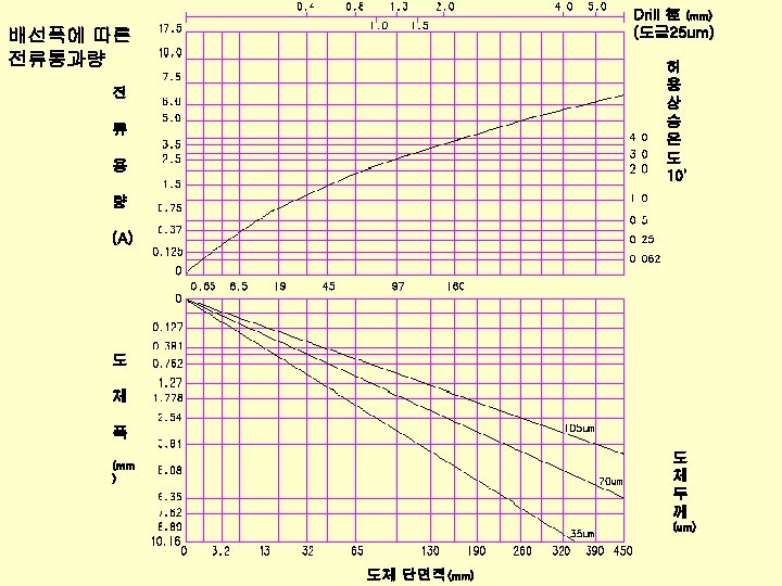
배선 기준표 항 목 Class 1 Class 2 Class 3 Class 4 Class 5 Class 6 배선 폭 배선간격 0. 3 0. 25 0. 2 0. 18 0. 16 0. 14 0. 15 0. 5 -1. 0 0. 125 0. 4 -0. 7 0. 1 0. 4 -0. 7 0. 09 0. 3 -0. 6 0. 08 0. 3 -0. 6 0. 07 0. 25 -0. 5 (최소도체간격) 배선 Grid 사용 Via (Drill-Land) * 위 배선폭은 설계시 CAD상의 설정치수이며 최종 제작된 PCB의 배선폭은 설계치보다 약 2/100 ~ 3/100 정도 작게 나온다. Via Land Via Drill 배선폭 A(Via-Pattern) A(Land-Land) A(Pattern-Pattern) A(Land-Pattern) 최소도체간격=A
Through Hole제작법 아래의 경우는 Drill Size 0. 9 일때의 기준이며 Land경과 Power경은 Drill Size의 크기에 따라 더하는 값은 비례적으로 적용한다. Drill Land Resist Power Drill경 : 부품 Pin의 굵기를 참조하여 설정(Normal: 0. 9) Land경 : Drill+0. 5 Resist경 : Land+0. 1 Power경 : Drill+0. 8
권장 표준 Through Hole Drill Land Resist Power 비고 0. 3 0. 4 0. 5 0. 7 0. 9 1. 0 1. 2 1. 5 2. 0 0. 6 0. 8 1. 0 1. 2 1. 4 1. 6 1. 8 2. 3 3. 0 0. 7 0. 9 1. 1 1. 3 1. 5 1. 7 1. 9 2. 4 3. 1 0. 8 1. 0 1. 2 1. 5 1. 7 2. 0 2. 2 2. 5 3. 2 Via용
None Through Hole제작법 Drill Resist 배선금지대 Resist경 : Drill+1. 0 Power경 : Drill+1. 5 배선금지대: Drill+2. 0 Power * NTH Mark : 모든 배선층에 공통으로 Drill Size보다 작은 2개의 Circle Line을 넣어둔다.
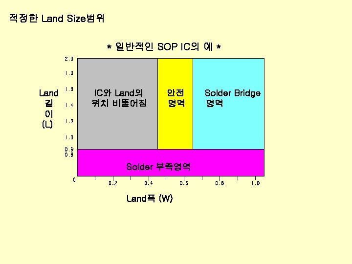
SMD Land Size P Land길이 : L+0. 6+0. 3 Land폭 : Pitch의 약 3/5로 한다. 길이 L W Pitch Width 0. 5 0. 65 1. 0 1. 27 0. 3 0. 4 0. 5 0. 6 0. 3 0. 6 폭
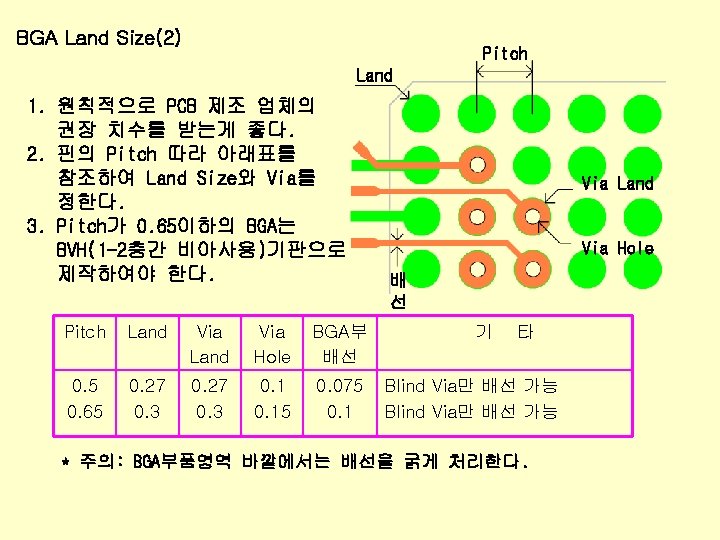
BGA Land Size(1) 부품 Pin의 Pitch에 따라 Land Size를 구하며 특히 부품 Catalog를 참조할 때 Top View인지 Bottom View인지 주의한다. Pitch Land * 도면의 Bottom View 표기 주의
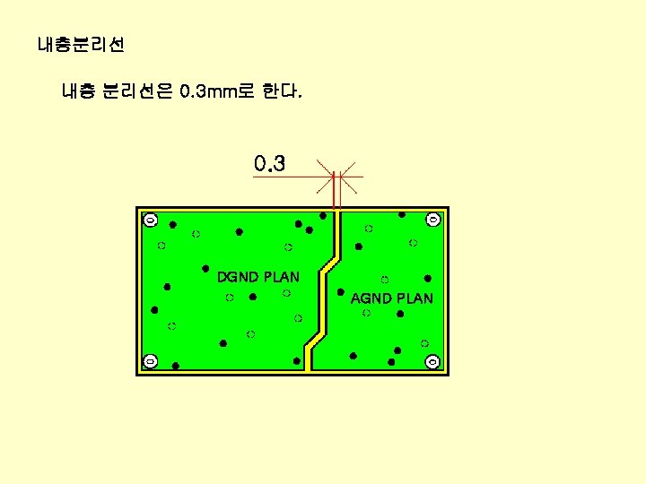
층 설정 * 상하 마주보는 층의 배선방향은 X, Y방향으로 교차할것. 1층 Comp(Top) 4층 2층 GND 3층 VCC 4층 Sold(Bottom) 1층 Comp(Top) 6층 2층 GND 3층 Signal(Int. 1) 4층 Signal(Int. 2) 5층 VCC 6층 Sold(Bottom) 6층(BVH) 1층 Comp(Top) 2층 Signal(Int. 1) 3층 GND 4층 VCC 5층 Signal(Int. 2) 6층 Sold(Bottom)
주요 Chip Pad Size (R, C, Tantal공통) 형 명 (Inch) 1005 1608 2012 3216 3225 3528 4532 5025 5832 6432 7343 (0402) (0603) (0805) (1206) (1201) (1411) (1812) (2012) (2312) (2512) (2917) Tantal P type A type B type C type D type A B C 0. 7 0. 9 1. 3 1. 7 1. 8 1. 9 2. 0 2. 3 2. 5 2. 4 0. 6 0. 8 1. 3 1. 8 2. 7 2. 8 3. 4 2. 7 2. 3 3. 4 3. 3 1. 1 1. 7 2. 3 3. 1 3. 2 3. 3 4. 5 5. 1 5. 3 6. 9 6. 5 A B C
SMD형 전해Cap Size 형명 Body(X, Y) D 55 E 55 F 60 H 63 H 10 J 10 3. 3 4. 3 5. 3 6. 6 8. 3 10. 3 x x x x 3. 3 4. 3 5. 3 6. 6 8. 3 10. 3 A B C 2. 5 2. 6 3. 0 3. 5 4. 2 4. 4 1. 0 1. 2 1. 5 2. 0 3. 2 3. 6 4. 4 5. 4 6. 8 7. 3 8. 9 A B Y X C
SMD IC Package 形名 1 SVP(Surface Vertical-Mount Package) SOP(Small Outline Package) TSOP(Thin Small Outline Package) SOJ(Small Outline J-lead Package)
SMD IC Package 形名 2 QFP(Quad Flat Package) QFJ(Quad Flat J-lead Package) LCC(Leadless Chip Carrier) LCC SOJ(Leaded Chip. Carrier SOJ) BGA(Ball Grid Array)
DIP IC Package 形名 SIP(Single Inline Package) ZIP(Zig-zag Inline Package) DIP(Dual Inline Package) PGA(Pin Grid Array)
QFP Library miss #6 73번에서 108번까지의 핀순서가 반대방향으로 설정되어 있 다. Go back check list shweee~
Chip dimension spec error 도면의 치수중 G부분이 0. 1 inch = 2. 54 mm이나 0. 1 inch = 1. 27 mm로 되어 있어 1. 27 mm로 설계불량 발 생.