CHARGE PUMP DESIGN FOR ULTRA LOW POWER PLLs
![Design 1: Charge Pump Without Compensation Method [4] Fig. 10: Schematic of the NMOS Design 1: Charge Pump Without Compensation Method [4] Fig. 10: Schematic of the NMOS](https://slidetodoc.com/presentation_image_h/324927a3f3f340ed55133c4c8a66a0ff/image-16.jpg)
![Design 1: Charge Pump Without Compensation Method [4] Results Fig. 11: Phase noise of Design 1: Charge Pump Without Compensation Method [4] Results Fig. 11: Phase noise of](https://slidetodoc.com/presentation_image_h/324927a3f3f340ed55133c4c8a66a0ff/image-17.jpg)
![VR Design 2: Charge Pump With Dual Compensation Method [4] VR Fig. 12: Schematic VR Design 2: Charge Pump With Dual Compensation Method [4] VR Fig. 12: Schematic](https://slidetodoc.com/presentation_image_h/324927a3f3f340ed55133c4c8a66a0ff/image-18.jpg)
![Design 2: Charge Pump With Dual Compensation Method [4] Result Fig. 14: Phase noise Design 2: Charge Pump With Dual Compensation Method [4] Result Fig. 14: Phase noise](https://slidetodoc.com/presentation_image_h/324927a3f3f340ed55133c4c8a66a0ff/image-20.jpg)
![Design 3: NMOS Topology Charge Pump [15] Fig. 15: Schematic of the NMOS charge Design 3: NMOS Topology Charge Pump [15] Fig. 15: Schematic of the NMOS charge](https://slidetodoc.com/presentation_image_h/324927a3f3f340ed55133c4c8a66a0ff/image-21.jpg)
![NMOS Topology Charge Pump [15] Result Fig. 16: Phase noise of the NMOS charge NMOS Topology Charge Pump [15] Result Fig. 16: Phase noise of the NMOS charge](https://slidetodoc.com/presentation_image_h/324927a3f3f340ed55133c4c8a66a0ff/image-22.jpg)
![Reference � [1] Woogeun Rhee, “Design of High – Performance CMOS Charge Pumps in Reference � [1] Woogeun Rhee, “Design of High – Performance CMOS Charge Pumps in](https://slidetodoc.com/presentation_image_h/324927a3f3f340ed55133c4c8a66a0ff/image-27.jpg)
![Reference (Cont. ) [8] Jean-François Richard and Yvon Savaria, “High Voltage Charge Pump Using Reference (Cont. ) [8] Jean-François Richard and Yvon Savaria, “High Voltage Charge Pump Using](https://slidetodoc.com/presentation_image_h/324927a3f3f340ed55133c4c8a66a0ff/image-28.jpg)
![Reference (Cont. ) � [17] C. M. Hung and K. K. O, “A fully Reference (Cont. ) � [17] C. M. Hung and K. K. O, “A fully](https://slidetodoc.com/presentation_image_h/324927a3f3f340ed55133c4c8a66a0ff/image-29.jpg)

- Slides: 30

CHARGE PUMP DESIGN FOR ULTRA - LOW POWER PLLs BY: R. F. ADDO 04/26/2011

OUTLINE Motivation � Introduction � Design Considerations for PLL’s Charge Pump v. Charge Sharing v. Charge Injection v. Clock Feedthrough v. Current Mismatch � Charge pump Designs v. Design 1: Current Steering NMOS Topology v. Design 2: Current Steering NMOS Topology With Dual Compensation method v. Design 3: NMOS Topology With No Current Steering v. Design 4: Novel Design � Simulation Results Summary and Conclusion � Reference � Questions �

MOTIVATION �The need for ultra – low power PLL has increased. �Depending on the type of VCO used, the charge pump contribute between 20 % to 50% of the total power consumption of the PLL �Reducing this power consumption will lead to a reduction of the overall power consumed by the PLL

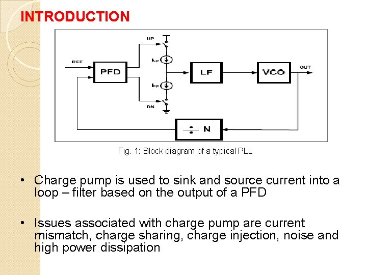
INTRODUCTION Fig. 1: Block diagram of a typical PLL • Charge pump is used to sink and source current into a loop – filter based on the output of a PFD • Issues associated with charge pump are current mismatch, charge sharing, charge injection, noise and high power dissipation

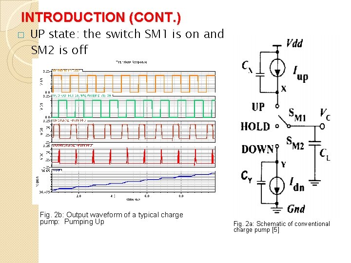
INTRODUCTION (CONT. ) � UP state: the switch SM 1 is on and SM 2 is off Fig. 2 b: Output waveform of a typical charge pump: Pumping Up Fig. 2 a: Schematic of conventional charge pump [5]

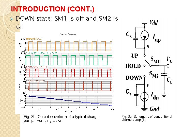
INTRODUCTION (CONT. ) Ø DOWN state: SM 1 is off and SM 2 is on Fig. 3 b: Output waveform of a typical charge pump: Pumping Down Fig. 3 a: Schematic of conventional charge pump [5]

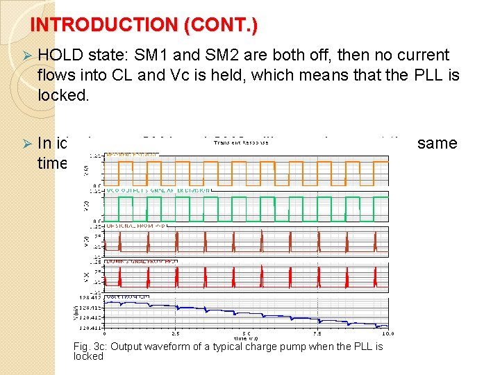
INTRODUCTION (CONT. ) Ø HOLD state: SM 1 and SM 2 are both off, then no current flows into CL and Vc is held, which means that the PLL is locked. Ø In ideal case, SM 1 and SM 2 will never be on at the same time. Fig. 3 c: Output waveform of a typical charge pump when the PLL is locked

Design Considerations For PLL’s Charge Pump Ø The necessary requirements for designing an effective charge pump circuit are: v Avoid the charge sharing; v Minimize the effect caused by charge injection and clock feed-through phenomena v Match the current values of Iup and Idn and make sure that there is no time mismatch between UP and DN. v Low power consumption

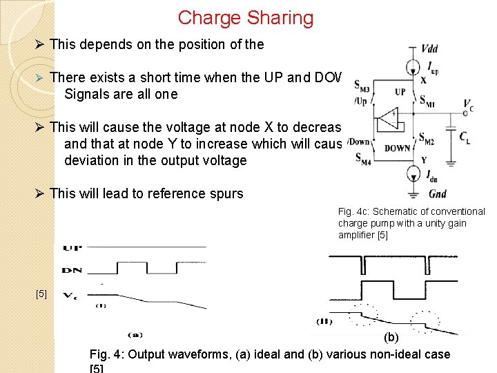
Charge Sharing Ø This depends on the position of the There exists a short time when the UP and DOWN Signals are all one Ø Ø This will cause the voltage at node X to decrease and that at node Y to increase which will cause a deviation in the output voltage Ø This will lead to reference spurs Fig. 4 c: Schematic of conventional charge pump with a unity gain amplifier [5] (b) Fig. 4: Output waveforms, (a) ideal and (b) various non-ideal case

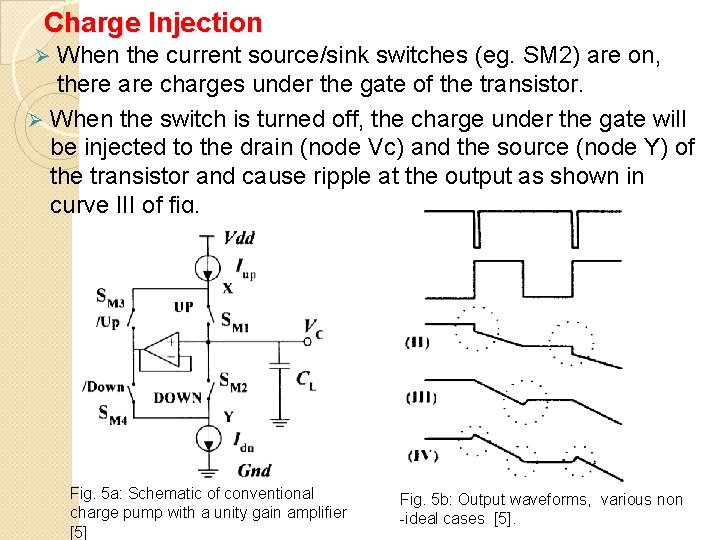
Charge Injection When the current source/sink switches (eg. SM 2) are on, there are charges under the gate of the transistor. Ø When the switch is turned off, the charge under the gate will be injected to the drain (node Vc) and the source (node Y) of the transistor and cause ripple at the output as shown in curve III of fig. Ø Fig. 5 a: Schematic of conventional charge pump with a unity gain amplifier [5] Fig. 5 b: Output waveforms, various non -ideal cases [5].

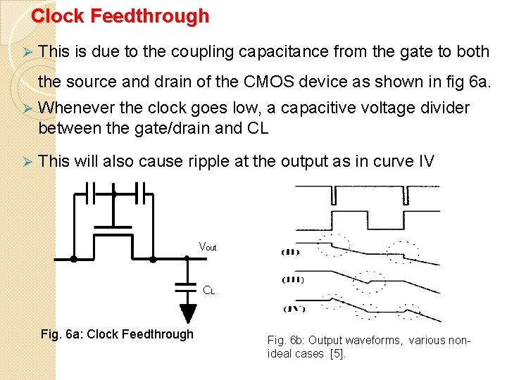
Clock Feedthrough Ø This is due to the coupling capacitance from the gate to both the source and drain of the CMOS device as shown in fig 6 a. Ø Whenever the clock goes low, a capacitive voltage divider between the gate/drain and CL Ø This will also cause ripple at the output as in curve IV Vout CL Fig. 6 a: Clock Feedthrough Fig. 6 b: Output waveforms, various nonideal cases [5].

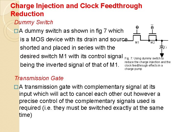
Charge Injection and Clock Feedthrough Reduction Dummy Switch � A dummy switch as shown in fig 7 which is a MOS device with its drain and source M 1 M 2 shorted and placed in series with the desired switch M 1 with its control signal Fig. 7: Using dummy switch to reduce the charge injection and the being the inverted signal of that of M 1. clock feedthrough effects in a charge pump Transmission Gate � A transmission gate with complementary signal at its input which will act to cancel each other out however a precise control of the complementary signals used is required (i. e. they must be switched exactly at the same time)

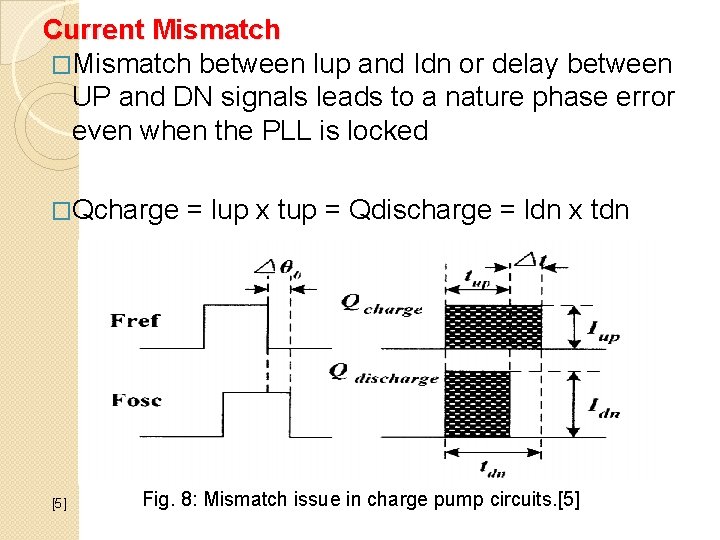
Current Mismatch �Mismatch between lup and Idn or delay between UP and DN signals leads to a nature phase error even when the PLL is locked �Qcharge = lup x tup = Qdischarge = ldn x tdn [5] Fig. 8: Mismatch issue in charge pump circuits. [5]

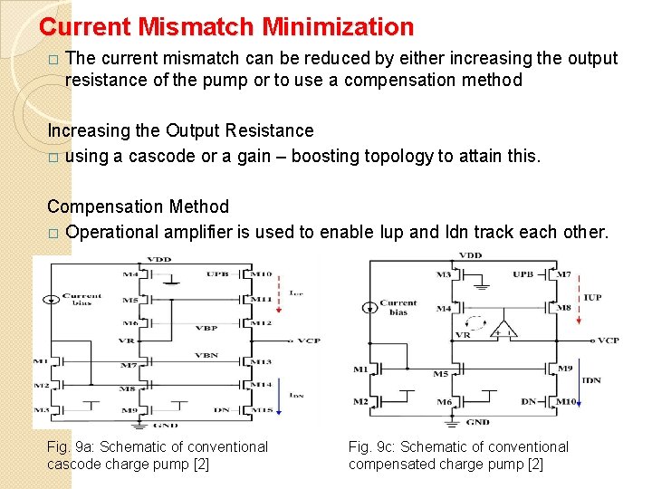
Current Mismatch Minimization � The current mismatch can be reduced by either increasing the output resistance of the pump or to use a compensation method Increasing the Output Resistance � using a cascode or a gain – boosting topology to attain this. Compensation Method � Operational amplifier is used to enable Iup and Idn track each other. Fig. 9 a: Schematic of conventional cascode charge pump [2] Fig. 9 c: Schematic of conventional compensated charge pump [2]

OUTLINE Motivation � Introduction � Design Considerations for PLL’s Charge Pump v. Charge Sharing v. Charge Injection v. Clock Feedthrough v. Current Mismatch � Charge pump Designs v. Design 1: Current Steering NMOS Topology v. Design 2: Current Steering NMOS Topology With Dual Compensation method v. Design 3: NMOS Topology With No Current Steering v. Design 4: Novel Design � Simulation Results Summary and Conclusion � Reference � Questions �
![Design 1 Charge Pump Without Compensation Method 4 Fig 10 Schematic of the NMOS Design 1: Charge Pump Without Compensation Method [4] Fig. 10: Schematic of the NMOS](https://slidetodoc.com/presentation_image_h/324927a3f3f340ed55133c4c8a66a0ff/image-16.jpg)
Design 1: Charge Pump Without Compensation Method [4] Fig. 10: Schematic of the NMOS charge pump without compensation � This design utilizes current steering switches to implement an NMOS topology charge pump
![Design 1 Charge Pump Without Compensation Method 4 Results Fig 11 Phase noise of Design 1: Charge Pump Without Compensation Method [4] Results Fig. 11: Phase noise of](https://slidetodoc.com/presentation_image_h/324927a3f3f340ed55133c4c8a66a0ff/image-17.jpg)
Design 1: Charge Pump Without Compensation Method [4] Results Fig. 11: Phase noise of the NMOS charge pump without compensation VDD (V) 0. 7 CURRENT MISMATCH PHASE NOISE (d. Bc/Hz) @ 1 MHz POWER @ 1 GHz (%) OFFSET 19. 13µW 1. 872 -104. 3
![VR Design 2 Charge Pump With Dual Compensation Method 4 VR Fig 12 Schematic VR Design 2: Charge Pump With Dual Compensation Method [4] VR Fig. 12: Schematic](https://slidetodoc.com/presentation_image_h/324927a3f3f340ed55133c4c8a66a0ff/image-18.jpg)
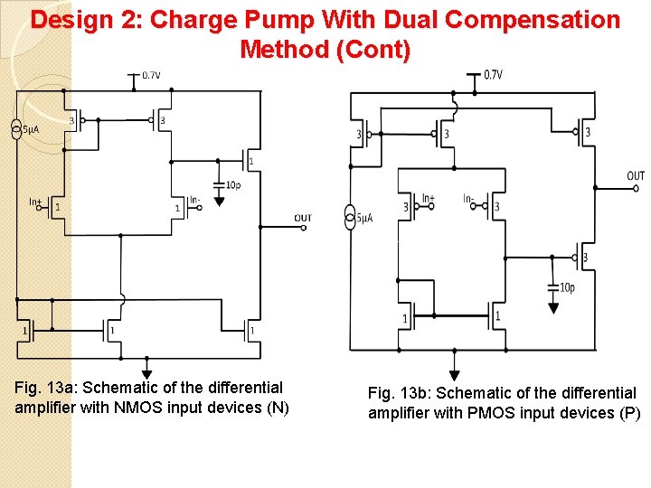
VR Design 2: Charge Pump With Dual Compensation Method [4] VR Fig. 12: Schematic of the NMOS charge pump with compensation � To minimize the current mismatch, two differential amplifiers are used � This gives an improvement in the current mismatch at the expense of power

Design 2: Charge Pump With Dual Compensation Method (Cont) Fig. 13 a: Schematic of the differential amplifier with NMOS input devices (N) Fig. 13 b: Schematic of the differential amplifier with PMOS input devices (P)
![Design 2 Charge Pump With Dual Compensation Method 4 Result Fig 14 Phase noise Design 2: Charge Pump With Dual Compensation Method [4] Result Fig. 14: Phase noise](https://slidetodoc.com/presentation_image_h/324927a3f3f340ed55133c4c8a66a0ff/image-20.jpg)
Design 2: Charge Pump With Dual Compensation Method [4] Result Fig. 14: Phase noise of the NMOS charge pump with compensation VDD (V) 0. 7 CURRENT MISMATCH PHASE NOISE (d. Bc/Hz) @ 1 MHz POWER @ 1 GHz (%) OFFSET 34. 42µW 0. 889 -101. 83
![Design 3 NMOS Topology Charge Pump 15 Fig 15 Schematic of the NMOS charge Design 3: NMOS Topology Charge Pump [15] Fig. 15: Schematic of the NMOS charge](https://slidetodoc.com/presentation_image_h/324927a3f3f340ed55133c4c8a66a0ff/image-21.jpg)
Design 3: NMOS Topology Charge Pump [15] Fig. 15: Schematic of the NMOS charge pump topology � This implements an NMOS topology charge pump � The difference between this design and that of designs 1 and 2 is that it does not use any current steering switches � It attains relatively good phase noise
![NMOS Topology Charge Pump 15 Result Fig 16 Phase noise of the NMOS charge NMOS Topology Charge Pump [15] Result Fig. 16: Phase noise of the NMOS charge](https://slidetodoc.com/presentation_image_h/324927a3f3f340ed55133c4c8a66a0ff/image-22.jpg)
NMOS Topology Charge Pump [15] Result Fig. 16: Phase noise of the NMOS charge pump topology VDD (V) 0. 7 CURRENT MISMATCH PHASE NOISE (d. Bc/Hz) @ 1 MHz POWER @ 1 GHz (%) OFFSET 18. 89µW -4. 68 -104. 35

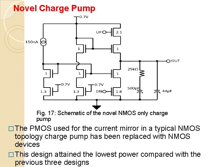
Novel Charge Pump Fig. 17: Schematic of the novel NMOS only charge pump � The PMOS used for the current mirror in a typical NMOS topology charge pump has been replaced with NMOS devices � This design attained the lowest power compared with the previous three designs

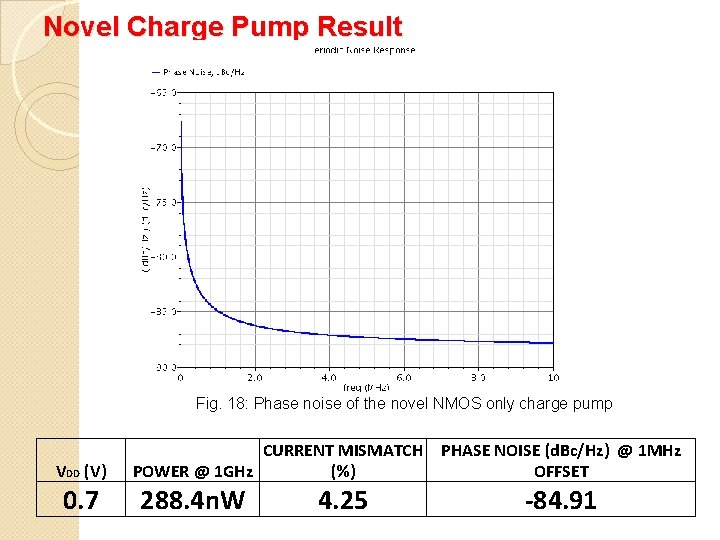
Novel Charge Pump Result Fig. 18: Phase noise of the novel NMOS only charge pump VDD (V) 0. 7 CURRENT MISMATCH PHASE NOISE (d. Bc/Hz) @ 1 MHz POWER @ 1 GHz (%) OFFSET 288. 4 n. W 4. 25 -84. 91

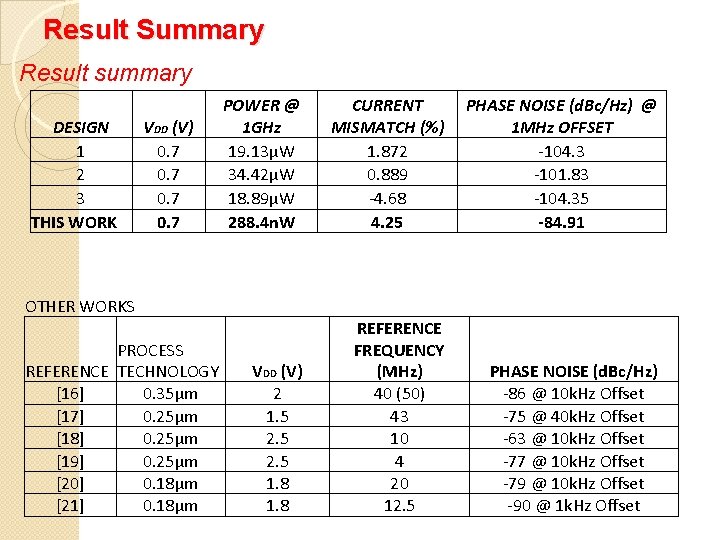
Result Summary Result summary DESIGN 1 2 3 THIS WORK VDD (V) 0. 7 POWER @ 1 GHz 19. 13µW 34. 42µW 18. 89µW 288. 4 n. W CURRENT MISMATCH (%) 1. 872 0. 889 -4. 68 4. 25 PHASE NOISE (d. Bc/Hz) @ 1 MHz OFFSET -104. 3 -101. 83 -104. 35 -84. 91 VDD (V) 2 1. 5 2. 5 1. 8 REFERENCE FREQUENCY (MHz) 40 (50) 43 10 4 20 12. 5 PHASE NOISE (d. Bc/Hz) -86 @ 10 k. Hz Offset -75 @ 40 k. Hz Offset -63 @ 10 k. Hz Offset -77 @ 10 k. Hz Offset -79 @ 10 k. Hz Offset -90 @ 1 k. Hz Offset OTHER WORKS PROCESS REFERENCE TECHNOLOGY [16] 0. 35µm [17] 0. 25µm [18] 0. 25µm [19] 0. 25µm [20] 0. 18µm [21] 0. 18µm

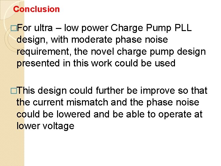
Conclusion �For ultra – low power Charge Pump PLL design, with moderate phase noise requirement, the novel charge pump design presented in this work could be used �This design could further be improve so that the current mismatch and the phase noise could be lowered and be able to operate at lower voltage
![Reference 1 Woogeun Rhee Design of High Performance CMOS Charge Pumps in Reference � [1] Woogeun Rhee, “Design of High – Performance CMOS Charge Pumps in](https://slidetodoc.com/presentation_image_h/324927a3f3f340ed55133c4c8a66a0ff/image-27.jpg)
Reference � [1] Woogeun Rhee, “Design of High – Performance CMOS Charge Pumps in Phase – locked loops. ” [2] Dong – Keon Lee, Jeong – Kwang Lee, and Hang – Geun Jeong, “A Dual – Compensated Charge Pump with Reduced Current Mismatch” � [3] M. -S. Hwang, J. Kim and D. -K. Jeong, “Reduction of pump current mismatch in charge-pump PLL” http: //ieeexplore. ieee. org/stamp. jsp? tp=&arnumber=4770439 � [4] Jae Hyung Noh, and Hang Geun Jeong, “Charge-Pump with a Regulated Cascode Circuit for Reducing Current Mismatch in PLLs” � [5] Hong Yut, Yasuaki Inouet, and Yan Han, “A New High-Speed Low. Voltage Charge Pump for PLL Applications” http: //ieeexplore. ieee. org/stamp. jsp? tp=&arnumber=1611344 � [6] Kyung-Soo Ha and Lee-Sup Kim, “Charge-Pump reducing current mismatch in DLLs and PLLs” http: //ieeexplore. ieee. org/stamp. jsp? tp=&arnumber=1693061 � [7] Shanfeng Cheng, Haitao Tong, Jose Silva-Martinez, and Aydin Ilker Karsilayan, “Design and Analysis of an Ultrahigh-Speed Glitch-Free Fully Differential Charge Pump With Minimum Output Current Variation and Accurate Matching” �
![Reference Cont 8 JeanFrançois Richard and Yvon Savaria High Voltage Charge Pump Using Reference (Cont. ) [8] Jean-François Richard and Yvon Savaria, “High Voltage Charge Pump Using](https://slidetodoc.com/presentation_image_h/324927a3f3f340ed55133c4c8a66a0ff/image-28.jpg)
Reference (Cont. ) [8] Jean-François Richard and Yvon Savaria, “High Voltage Charge Pump Using Standard CMOS Technology” � [9] Janusz A. Starzyk, Ying-Wei Jan, and Fengjing Qiu, “A DC–DC Charge Pump Design Based on Voltage Doublers” � [10] Nick Van Helleputte and Georges Gielen “An Ultra-low-Power Quadrature PLL in 130 nm CMOS for Impulse Radio Receivers” http: //ieeexplore. ieee. org/stamp. jsp? tp=&arnumber=4463309&ta g=1 � [11] Q. Guo, H. F. Zhou, W. W. Cheng, Y. Han, X. X. Han, and X. Liang, “A Low Phase-noise Low-power PLL in 0. 13 -¹m CMOS for Low Voltage Application” � [12] Gong Zhichao, Lu Lei, Liao Youchun, and Tang Zhangwen, “Design and noise analysis of a fully-differential charge pump for phase -locked loops” � [13] Po-Yao Ke and Jon Guerber, “A 1. 3 V Low Power Divide by 4 PLL Design with Output Range 0. 5 GHz-1. 5 GHz” � [14] Partha Pratim Ghosh, “ Design and Study of Phase Locked Loop for Space Applications In Submicron CMOS Technology” � [15] Tsan – Huei Wu, “ Low – Cost Jitter Measurement Techniques for Phase Locked Loops. ” � [16] Keliu Shu, Edgar Sanchez – Sinencio, Jose Silva – Martinez, and Sherif H. K. Embabi, “A 2. 4 – GHz monolithic fractional – N frequency synthesizer with robust phase – switching prescaler and loop �
![Reference Cont 17 C M Hung and K K O A fully Reference (Cont. ) � [17] C. M. Hung and K. K. O, “A fully](https://slidetodoc.com/presentation_image_h/324927a3f3f340ed55133c4c8a66a0ff/image-29.jpg)
Reference (Cont. ) � [17] C. M. Hung and K. K. O, “A fully integrated 1. 5 – V 5. 5 – GHz CMOS phase – locked loop” [18] S. Pellerano, S. Laventino, C. Samori, and A. Lacaita, “A 13. 5 – m. W 5 -GHz frequency synthesizer with dynamic – logic frequency divider” � [19] F. Herzel, G. Fischer, and P. Weger, “An integrated CMOS RF synthesizer for 802. 11 a wireless LAN” � [20] Chun – Yi Kuo, Jung – Yu Chang, and Shen – Iuan Lui, “A spur – reduction technique for a 5 – GHz frequency synthesizer” � � [21] A fully differential charge pump with accurate current matching and rail – to – rail common – mode feedback circuit. ” BOOKS: � Low – Voltage CMOS RF Frequency Synthesizers by Howard C. Luong and Gerry C. T. Leung � High Speed CMOS Circuits for Optical Receivers by Jafar Savoj and Behzad Razavi �PLL Performance, Simulation and Design by Dean Banerjee

QUESTIONS