Charge multiplication in radiationdamaged epitaxial silicon detectors Jrn
- Slides: 27

Charge multiplication in radiation-damaged epitaxial silicon detectors Jörn Lange 1, Alexandra Junkes 1, Julian Becker 1, Eckhart Fretwurst 1, Robert Klanner 1, Gunnar Lindström 1, Ioana Pintilie 2 1 University of Hamburg 2 NIMP Bucharest 12 th Vienna Conference on Instrumentation, February 2010 In the framework of the CERN RD 50 Collaboration

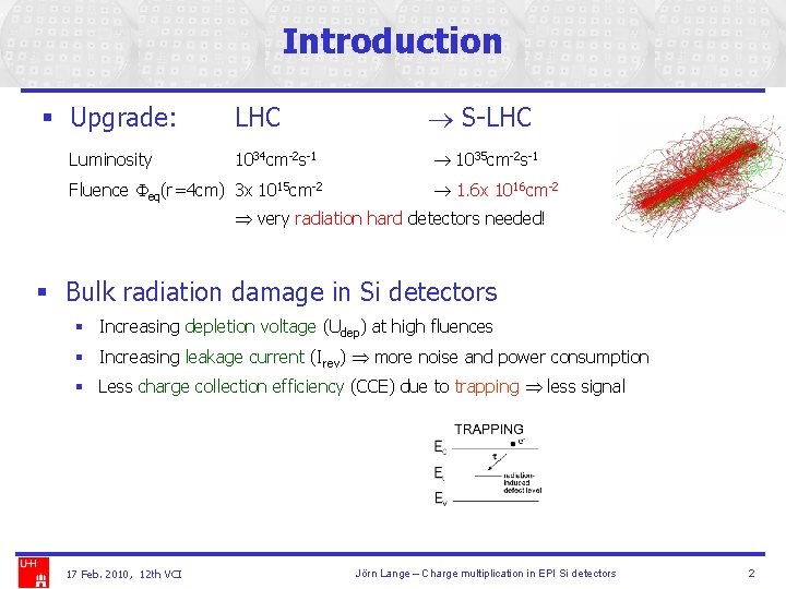
Introduction § Upgrade: Luminosity LHC 1034 cm-2 s-1 Fluence Feq(r=4 cm) 3 x 1015 cm-2 S-LHC 1035 cm-2 s-1 1. 6 x 1016 cm-2 very radiation hard detectors needed! § Bulk radiation damage in Si detectors § Increasing depletion voltage (Udep) at high fluences § Increasing leakage current (Irev) more noise and power consumption § Less charge collection efficiency (CCE) due to trapping less signal 17 Feb. 2010, 12 th VCI Jörn Lange – Charge multiplication in EPI Si detectors 2

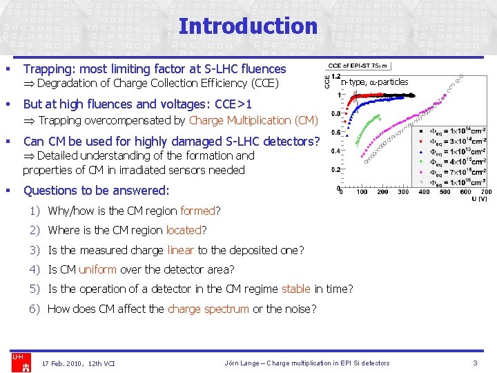
Introduction § Trapping: most limiting factor at S-LHC fluences Degradation of Charge Collection Efficiency (CCE) § n-type, a-particles But at high fluences and voltages: CCE>1 Trapping overcompensated by Charge Multiplication (CM) § Can CM be used for highly damaged S-LHC detectors? Detailed understanding of the formation and properties of CM in irradiated sensors needed § Questions to be answered: 1) Why/how is the CM region formed? 2) Where is the CM region located? 3) Is the measured charge linear to the deposited one? 4) Is CM uniform over the detector area? 5) Is the operation of a detector in the CM regime stable in time? 6) How does CM affect the charge spectrum or the noise? 17 Feb. 2010, 12 th VCI Jörn Lange – Charge multiplication in EPI Si detectors 3

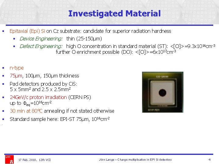
Investigated Material § Epitaxial (Epi) Si on Cz substrate: candidate for superior radiation hardness § Device Engineering: thin (25 -150µm) § Defect Engineering: high O concentration in standard material (ST): <[O]>=9. 3 x 10 16 cm-3 further O enrichment possible (DO): <[O]>=6 x 1017 cm-3 § n-type § 75µm, 100µm, 150µm thickness § Pad detectors produced by Ci. S: 5 x 5 mm 2 and 2. 5 x 2. 5 mm 2 § 24 Ge. V/c proton irradiation (CERN PS) up to Feq=1016 cm-2 § 30 min at 80°C annealing if not stated otherwise § Standard sample here: EPI-ST 75µm, 1016 cm-2 § 17 Feb. 2010, 12 th VCI Jörn Lange – Charge multiplication in EPI Si detectors 4

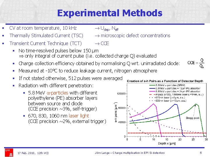
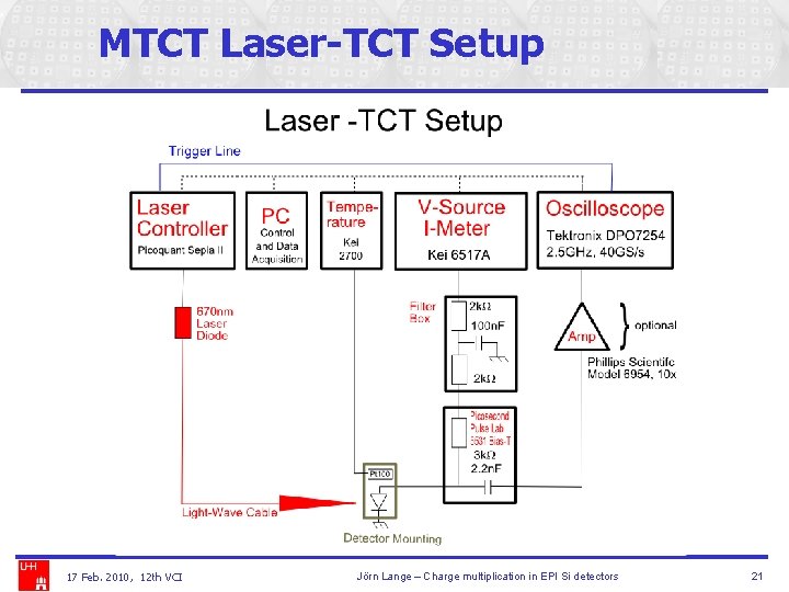
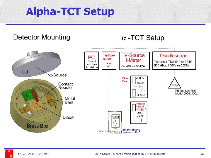
Experimental Methods § CV at room temperature, 10 k. Hz Udep, Neff § Thermally Stimulated Current (TSC) microscopic defect concentrations § Transient Current Technique (TCT) CCE § No time-resolved pulses below 150 µm only integral of current pulse (i. e. collected charge Q) evaluated § Charge collection efficiency obtained by normalising Q wrt. unirradiated diode: § Measured at -10°C to reduce leakage current, nitrogen atmosphere § If not stated otherwise, 512 pulses were averaged § Radiation with different penetration: § 5. 8 Me. V a-particles with different polyethylene (PE) absorber layers between source and diode (CCE precision ~3%, self-trigger) § 670, 830, 1060 nm laser light (CCE precision ~2%, external trigger) 17 Feb. 2010, 12 th VCI Jörn Lange – Charge multiplication in EPI Si detectors 5

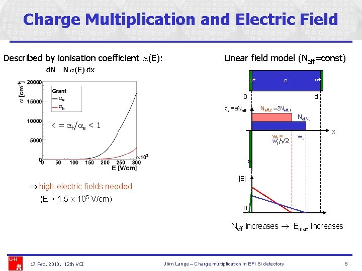
Charge Multiplication and Electric Field Described by ionisation coefficient a(E): Linear field model (Neff=const) p+ n+ n 0 d rel=e. Neff, 2 =2 Neff, 1 k = ah/ae < 1 w 2= w 1/√ 2 w 1 x high electric fields needed |E| (E > 1. 5 x 10⁵ V/cm) 0 Neff increases Emax increases 17 Feb. 2010, 12 th VCI Jörn Lange – Charge multiplication in EPI Si detectors 6

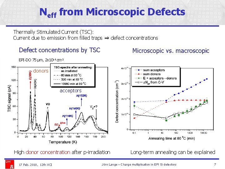
Neff from Microscopic Defects Thermally Stimulated Current (TSC): Current due to emission from filled traps ⇒ defect concentrations Defect concentrations by TSC Microscopic vs. macroscopic EPI-DO 75 µm, 2 x 1014 cm-2 donors acceptors High donor concentration after p-irradiation 17 Feb. 2010, 12 th VCI Long-term annealing can be explained Jörn Lange – Charge multiplication in EPI Si detectors 7

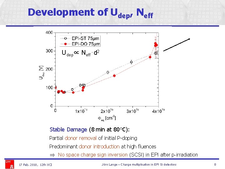
Development of Udep, Neff Udep∝ Neff⋅d 2 Stable Damage (8 min at 80°C): Partial donor removal of initial P-doping Predominant donor introduction at high fluences No space charge sign inversion (SCSI) in EPI after p-irradiation 17 Feb. 2010, 12 th VCI Jörn Lange – Charge multiplication in EPI Si detectors 8

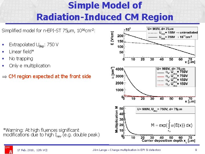
Simple Model of Radiation-Induced CM Region Simplified model for n-EPI-ST 75µm, 1016 cm-2: § § Extrapolated Udep: 750 V Linear field* No trapping Only e multiplication CM region expected at the front side *Warning: At high fluences significant modifications due to high Irev (e. g. double peak) 17 Feb. 2010, 12 th VCI Jörn Lange – Charge multiplication in EPI Si detectors 9

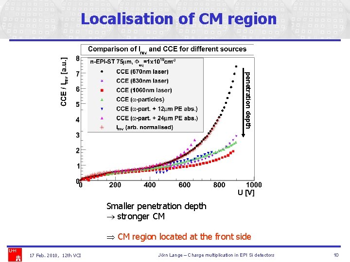
Localisation of CM region penetration depth Smaller penetration depth stronger CM region located at the front side 17 Feb. 2010, 12 th VCI Jörn Lange – Charge multiplication in EPI Si detectors 10

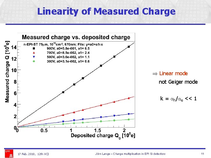
Linearity of Measured Charge Linear mode not Geiger mode k = ah/ae << 1 17 Feb. 2010, 12 th VCI Jörn Lange – Charge multiplication in EPI Si detectors 11

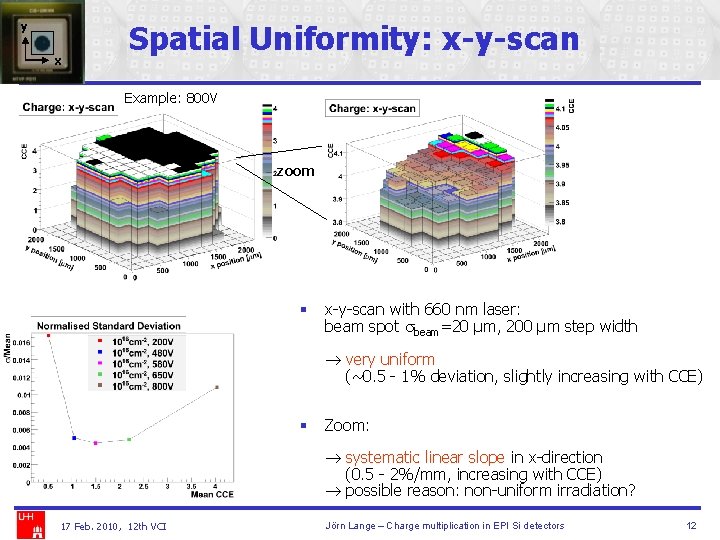
y x Spatial Uniformity: x-y-scan Example: 800 V zoom § x-y-scan with 660 nm laser: beam spot sbeam=20 µm, 200 µm step width very uniform (~0. 5 - 1% deviation, slightly increasing with CCE) § Zoom: systematic linear slope in x-direction (0. 5 - 2%/mm, increasing with CCE) possible reason: non-uniform irradiation? 17 Feb. 2010, 12 th VCI Jörn Lange – Charge multiplication in EPI Si detectors 12

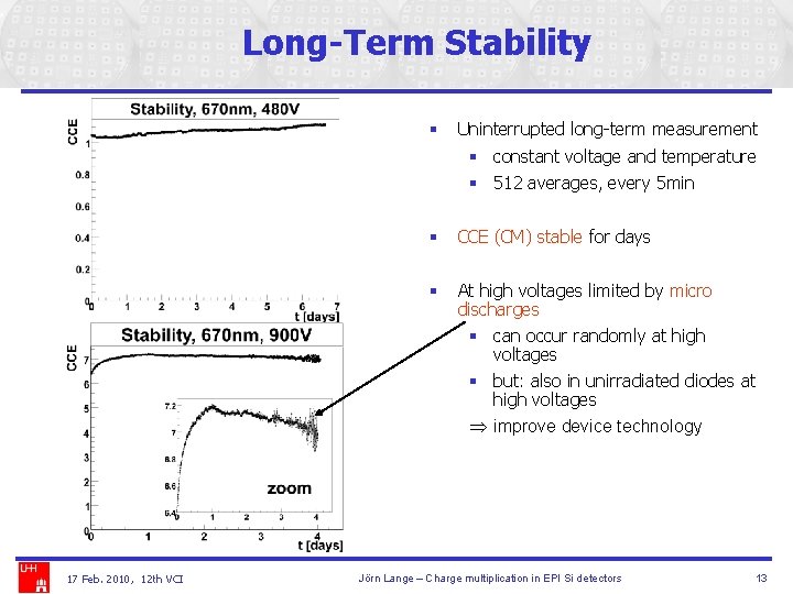
Long-Term Stability § Uninterrupted long-term measurement § constant voltage and temperature § 512 averages, every 5 min § CCE (CM) stable for days § At high voltages limited by micro discharges § can occur randomly at high voltages § but: also in unirradiated diodes at high voltages improve device technology 17 Feb. 2010, 12 th VCI Jörn Lange – Charge multiplication in EPI Si detectors 13

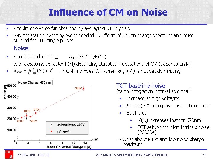
Influence of CM on Noise § § Results shown so far obtained by averaging 512 signals S/N separation event by event needed Effects of CM on charge spectrum and noise studied for 300 single pulses Noise: § Shot noise due to Irev: sshot ~ M' ·√F(M') with excess noise factor F(M) describing statistical fluctuations of CM (depends on k) CM improves S/N when sshot(M') is not yet dominating § 900 V 480 V 200 V 650 V 580 V TCT baseline noise (same integration interval as signal) § § § Increase at high voltages Signal (670 nm) grows faster than noise But here: § § M(U) increases fast for 670 nm TCT setup with high intrinsic noise (20000 e) What about MIPs and low noise charge readout? 17 Feb. 2010, 12 th VCI Jörn Lange – Charge multiplication in EPI Si detectors 14

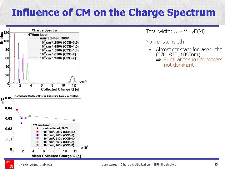
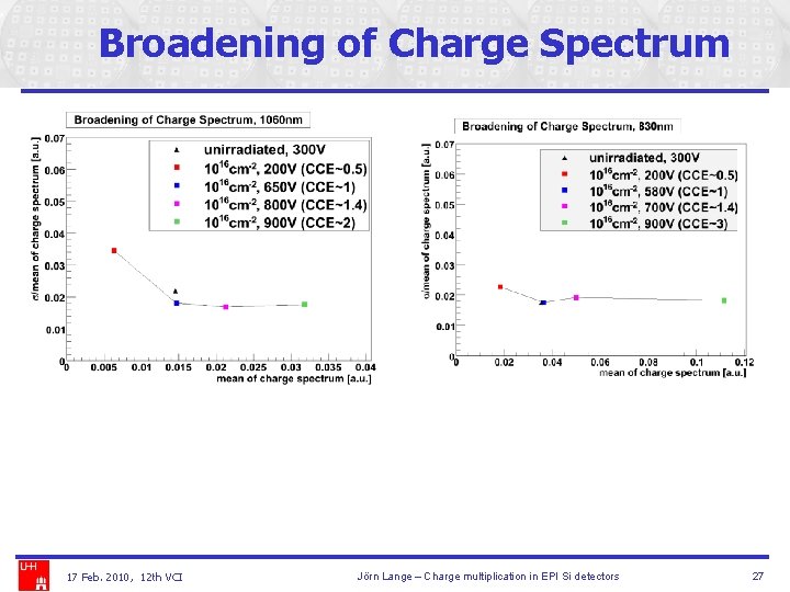
Influence of CM on the Charge Spectrum Total width: s ~ M ·√F(M) Normalised width: § Almost constant for laser light (670, 830, 1060 nm) Fluctuations in CM process not dominant 17 Feb. 2010, 12 th VCI Jörn Lange – Charge multiplication in EPI Si detectors 15

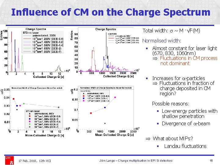
Influence of CM on the Charge Spectrum Total width: s ~ M ·√F(M) Normalised width: § Almost constant for laser light (670, 830, 1060 nm) Fluctuations in CM process not dominant § Increases for a-particles Fluctuations in fraction of charge deposited in CM region? Possible reasons: § Low-energy particles with shallow penetration § Divergence of a-beam What about MIPs? § 17 Feb. 2010, 12 th VCI Landau fluctuations Jörn Lange – Charge multiplication in EPI Si detectors 16

Summary and Outlook § Charge Multiplication in highly irradiated n-EPI diodes: § § § High field at the front side due to radiation-induced predominant donor introduction Linear mode Uniform over the detector area, stable in time Noise increase slower than signal growth (TCT with 670 nm laser) No significant fluctuations in CM process § Open issues: § S/N for MIPs and charge readout Charge measurements with beta-setup in progress § Can micro discharges at high voltages be reduced and controlled? § Possible effects on position resolution segmented sensors Charge multiplication seems to be a promising candidate to overcome trapping in highly irradiated detectors 17 Feb. 2010, 12 th VCI Jörn Lange – Charge multiplication in EPI Si detectors 17

BACKUP SLIDES 17 Feb. 2010, 12 th VCI Jörn Lange – Charge multiplication in EPI Si detectors 18

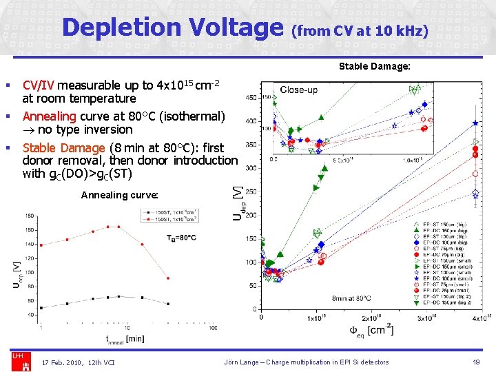
Depletion Voltage (from CV at 10 k. Hz) Stable Damage: § CV/IV measurable up to 4 x 1015 cm-2 at room temperature § Annealing curve at 80°C (isothermal) no type inversion § Stable Damage (8 min at 80°C): first donor removal, then donor introduction with g. C(DO)>g. C(ST) Annealing curve: 17 Feb. 2010, 12 th VCI Jörn Lange – Charge multiplication in EPI Si detectors 19

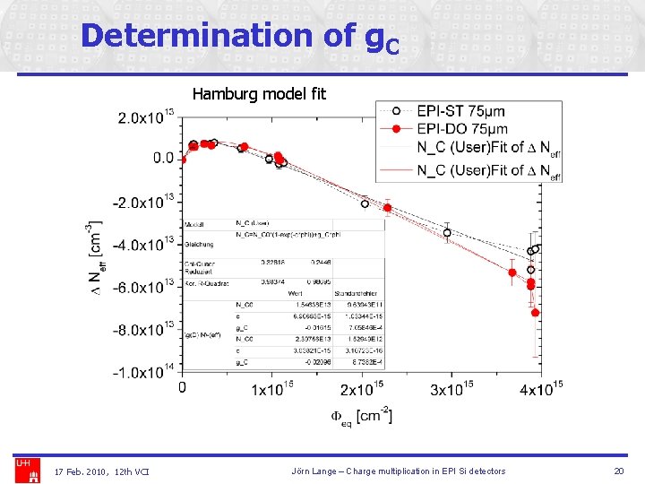
Determination of g. C Hamburg model fit 17 Feb. 2010, 12 th VCI Jörn Lange – Charge multiplication in EPI Si detectors 20

MTCT Laser-TCT Setup 17 Feb. 2010, 12 th VCI Jörn Lange – Charge multiplication in EPI Si detectors 21

Alpha-TCT Setup 17 Feb. 2010, 12 th VCI Jörn Lange – Charge multiplication in EPI Si detectors 22

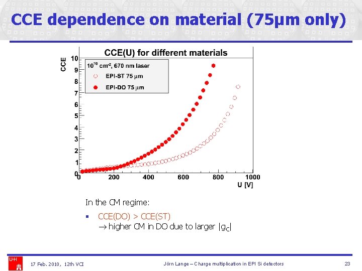
CCE dependence on material (75µm only) In the CM regime: § 17 Feb. 2010, 12 th VCI CCE(DO) > CCE(ST) higher CM in DO due to larger |g. C| Jörn Lange – Charge multiplication in EPI Si detectors 23

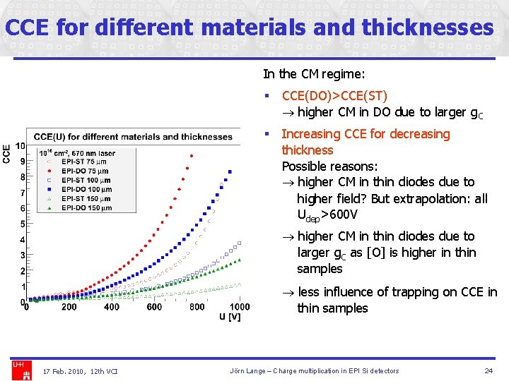
CCE for different materials and thicknesses In the CM regime: § CCE(DO)>CCE(ST) higher CM in DO due to larger g. C § Increasing CCE for decreasing thickness Possible reasons: higher CM in thin diodes due to higher field? But extrapolation: all Udep>600 V higher CM in thin diodes due to larger g. C as [O] is higher in thin samples less influence of trapping on CCE in thin samples 17 Feb. 2010, 12 th VCI Jörn Lange – Charge multiplication in EPI Si detectors 24

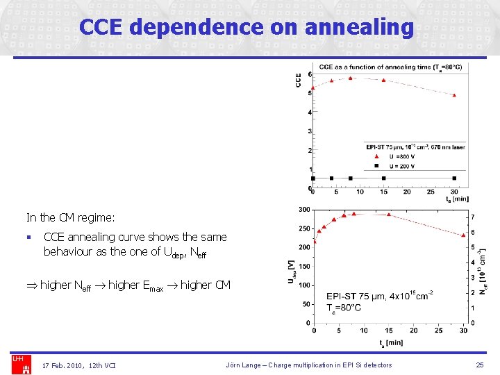
CCE dependence on annealing In the CM regime: § CCE annealing curve shows the same behaviour as the one of Udep, Neff higher Emax higher CM 17 Feb. 2010, 12 th VCI Jörn Lange – Charge multiplication in EPI Si detectors 25

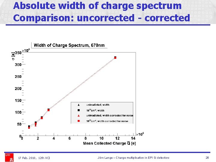
Absolute width of charge spectrum Comparison: uncorrected - corrected 17 Feb. 2010, 12 th VCI Jörn Lange – Charge multiplication in EPI Si detectors 26

Broadening of Charge Spectrum 17 Feb. 2010, 12 th VCI Jörn Lange – Charge multiplication in EPI Si detectors 27