Characterization of Magnetic Thin Films using the Magneto


 Polarized Light Beam Change in Polarization Initial Polarization Sample")
")


 2000 1000 0 -4 -3 -2 -1 0")


- Slides: 17
Characterization of Magnetic Thin Films using the Magneto Optic Kerr Effect Nicholas J. Savino Lynchburg College Department of Physics
Magnetization "Hysteresis Loop and Magnetic Properties. " NDT Resource Center. NSF-ATE, n. d. Web.
Magneto Optic Kerr Effect (MOKE) Polarized Light Beam Change in Polarization Initial Polarization Sample Kerr, John. “XLIII. On Rotation of the Plane of Polarization by Reflection from the Pole of a Magnet. ” Philosophical Magazine, vol. 3, no. 19, ser. 5, 1877, pp. 321– 343. Davidson, Michael W. “John Kerr. ” Molecular Expressions: Science, Optics and You, National High Magnetic Field Laboratory, 13 Nov. 2015.
Thin Films Thin film of Ni and Fe. Pd (40 to 400 nm thick) Si wafer (0. 1 to 1 mm thick)
Laser Photodetector Polarizer Chopper Analyzer Electromagnet Crossed Polarizers
"Hysteresis Loop and Magnetic Properties. " NDT Resource Center. NSF-ATE, n. d. Web.
Data Hysteresis loop created by the Ni sample Hysteresis loop created by the Fe. Pd sample
Applications Biebel , Harald. “Brilliant Hard Drive Quality with Magnetic Field Sensors Made of Diamond. ” Phys. org, Fraunhofer Gesellschaft, 30 June 2016.
Future Work More samples • Cooling system allowing stronger magnetic field • Applying fields at different orientations • B B R. A. Lukaszew et al. / Applied Surface Science 219 (2003)
Acknowledgements Lukaszew Research Group at College of William and Mary, provided Fe. Pd capped with Au sample • Dr. William Roach, research advisor • New. Market Corporation, Virginia Foundation for Independent Colleges, Summer Undergraduate Science Research Fellowship •
Questions?
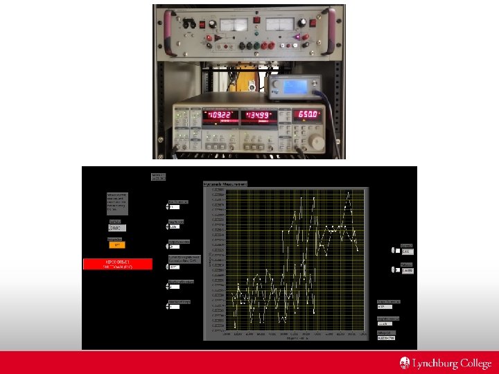
Lab. VIEW Block Diagram
Calibration 4000 3000 Magnetic field (G) 2000 1000 0 -4 -3 -2 -1 0 -1000 -2000 -3000 -4000 Current (A) 1 2 3 4
Methodology Lock-in and chopper set to 650 Hz • Polarizer oriented at approximately 320 degrees, analyzer oriented at approximately 170 degrees, nearly crossing the two • The samples tested were: – 100 nm Ni thin film sample on Si wafer (Ni) – 100 nm Ni thin film sample on 300 nm Si. O 2 on Si wafer (Ni on Si. O 2) – 40 nm Fe. Pd thin film sample capped with 5 nm Au (Fe. Pd capped with Au) •
Comparing Orientations Hysteresis loops created by Ni sample in orientation 1 in blue, orientation 2 in orange Hysteresis loops created by Ni (on Si. O 2)sample in orientation 2 in black, orientation 1 in red
Thank you!