Characterization of inner layer sensors D Inner Layer
- Slides: 24

Characterization of inner layer sensors DØ Inner Layer Sensor Production Readiness Review FNAL, 8/8/2003 M. Demarteau, R. Demina, S. Korjenevski, F. Lehner, R. Lipton, H. S. Mao, B. Mc. Carthy, R. Smith Frank Lehner U Zurich

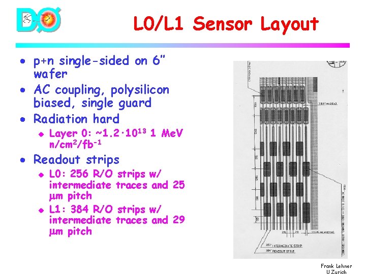
L 0/L 1 Sensor Layout · p+n single-sided on 6’’ wafer · AC coupling, polysilicon biased, single guard · Radiation hard u Layer 0: ~1. 2· 1013 1 Me. V n/cm 2/fb-1 · Readout strips u u L 0: 256 R/O strips w/ intermediate traces and 25 m pitch L 1: 384 R/O strips w/ intermediate traces and 29 m pitch Frank Lehner U Zurich

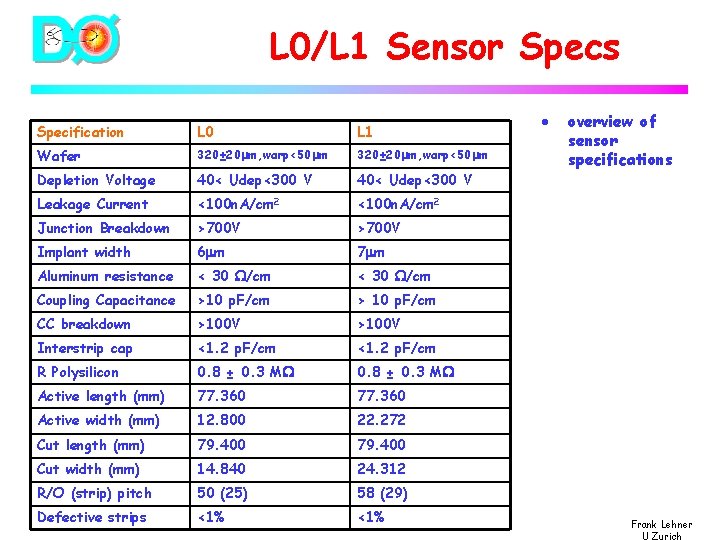
L 0/L 1 Sensor Specs Specification L 0 L 1 Wafer 320± 20 m, warp<50 m Depletion Voltage 40< Udep<300 V Leakage Current <100 n. A/cm 2 Junction Breakdown >700 V Implant width 6 m 7 m Aluminum resistance < 30 /cm Coupling Capacitance >10 p. F/cm > 10 p. F/cm CC breakdown >100 V Interstrip cap <1. 2 p. F/cm R Polysilicon 0. 8 ± 0. 3 M Active length (mm) 77. 360 Active width (mm) 12. 800 22. 272 Cut length (mm) 79. 400 Cut width (mm) 14. 840 24. 312 R/O (strip) pitch 50 (25) 58 (29) Defective strips <1% · overview of sensor specifications Frank Lehner U Zurich

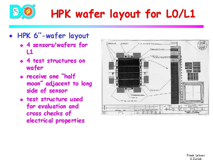
HPK wafer layout for L 0/L 1 · HPK 6’’-wafer layout u u 4 sensors/wafers for L 1 4 test structures on wafer receive one “half moon” adjacent to long side of sensor test structure used for evaluation and cross checks of electrical properties Frank Lehner U Zurich

HPK layer 1 production · Procurement strategy: u u ordered only layer 1 prototypes for qualification layer 0 very similar, but detailed drawings were not ready so early due to complicated layout w/ analog cable · 10 prototypes for layer 1 ordered in April 2002, shipped to FNAL in Sept 2002 u u extensively tested 3 of them irradiated · 3 more prototypes ordered in May 2003, shipped to FNAL in July 2003 u testing results included in PRR document/talk · rough estimate of “yield”, based on serial numbering ~54%, lower than for outer layer sensors (~70%) · HPK QA: 2 (out of 13) had one defect, 1 (out of 13) had two defects Frank Lehner U Zurich

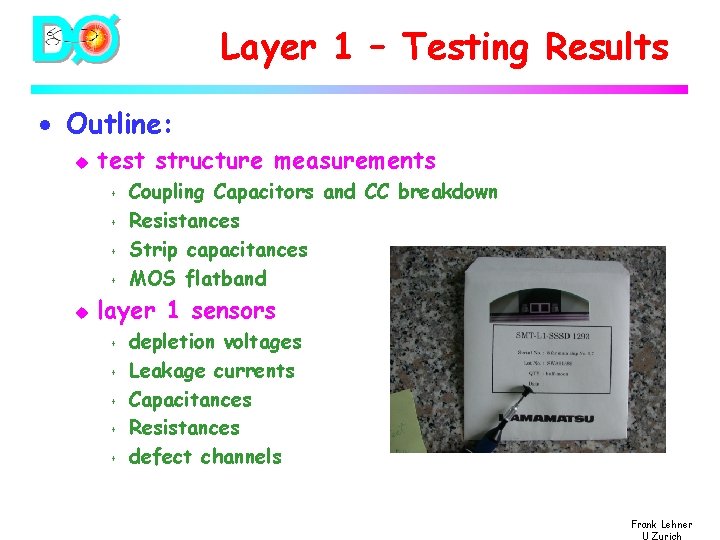
Layer 1 – Testing Results · Outline: u test structure measurements s s u Coupling Capacitors and CC breakdown Resistances Strip capacitances MOS flatband layer 1 sensors s s depletion voltages Leakage currents Capacitances Resistances defect channels Frank Lehner U Zurich

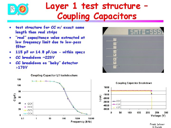
Layer 1 test structure – Coupling Capacitors · · · test structure for CC w/ exact same length than real strips “real” capacitance value extracted at low frequency limit due to low-pass filter 115 p. F or 14. 8 p. F/cm - within specs CC breakdown ~220 V CC breakdown on “baby” detector >170 V Frank Lehner U Zurich

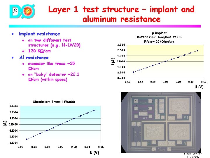
Layer 1 test structure – implant and aluminum resistance · implant resistance u u · on two different test structures (e. g. N-LW 20) 130 K /cm Al resistance u u meander like trace ~35 /cm on “baby” detector ~22. 1 /cm (within specs) Frank Lehner U Zurich

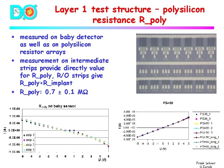
Layer 1 test structure – polysilicon resistance R_poly · measured on baby detector as well as on polysilicon resistor arrays · measurement on intermediate strips provide directly value for R_poly, R/O strips give R_poly+R_implant · R_poly: 0. 7 ± 0. 1 M Frank Lehner U Zurich

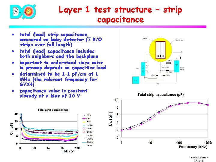
Layer 1 test structure – strip capacitance · · · total (load) strip capacitance measured on baby detector (7 R/O strips over full length) total (load) capacitance includes both neighbors and the backplane important to understand since noise in preamp depends on capacitive load determined to be 1. 1 p. F/cm at 1 MHz (the relevant frequency for SVX 4) capacitance value is constant already at a bias of 10 V Frank Lehner U Zurich

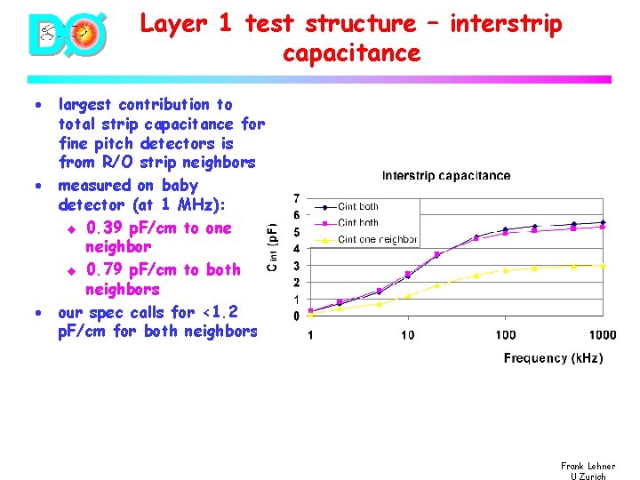
Layer 1 test structure – interstrip capacitance · · · largest contribution to total strip capacitance for fine pitch detectors is from R/O strip neighbors measured on baby detector (at 1 MHz): u 0. 39 p. F/cm to one neighbor u 0. 79 p. F/cm to both neighbors our spec calls for <1. 2 p. F/cm for both neighbors Frank Lehner U Zurich

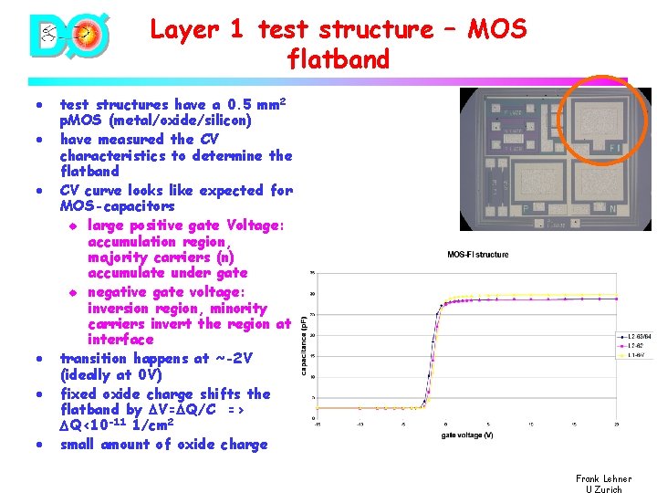
Layer 1 test structure – MOS flatband · · · test structures have a 0. 5 mm 2 p. MOS (metal/oxide/silicon) have measured the CV characteristics to determine the flatband CV curve looks like expected for MOS-capacitors u large positive gate Voltage: accumulation region, majority carriers (n) accumulate under gate u negative gate voltage: inversion region, minority carriers invert the region at interface transition happens at ~-2 V (ideally at 0 V) fixed oxide charge shifts the flatband by V= Q/C => Q<10 -11 1/cm 2 small amount of oxide charge Frank Lehner U Zurich

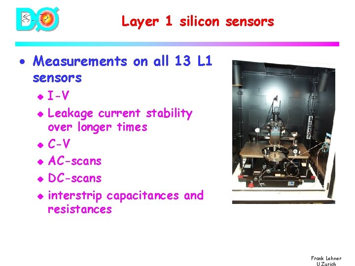
Layer 1 silicon sensors · Measurements on all 13 L 1 sensors u u u I-V Leakage current stability over longer times C-V AC-scans DC-scans interstrip capacitances and resistances Frank Lehner U Zurich

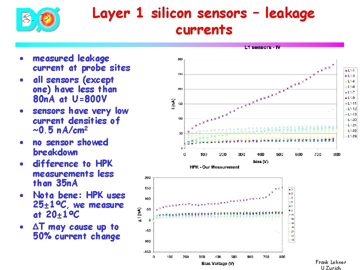
Layer 1 silicon sensors – leakage currents · · · · measured leakage current at probe sites all sensors (except one) have less than 80 n. A at U=800 V sensors have very low current densities of ~0. 5 n. A/cm 2 no sensor showed breakdown difference to HPK measurements less than 35 n. A Nota bene: HPK uses 25± 1ºC, we measure at 20± 1ºC T may cause up to 50% current change Frank Lehner U Zurich

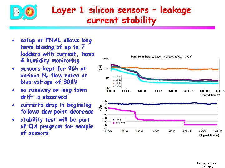
Layer 1 silicon sensors – leakage current stability · · · setup at FNAL allows long term biasing of up to 7 ladders with current, temp & humidity monitoring sensors kept for 96 h at various N 2 flow rates at bias voltage of 300 V no runaway or long term drift is observed currents drop in beginning follows dew point decrease stability test will be part of QA program for sample of sensors Frank Lehner U Zurich

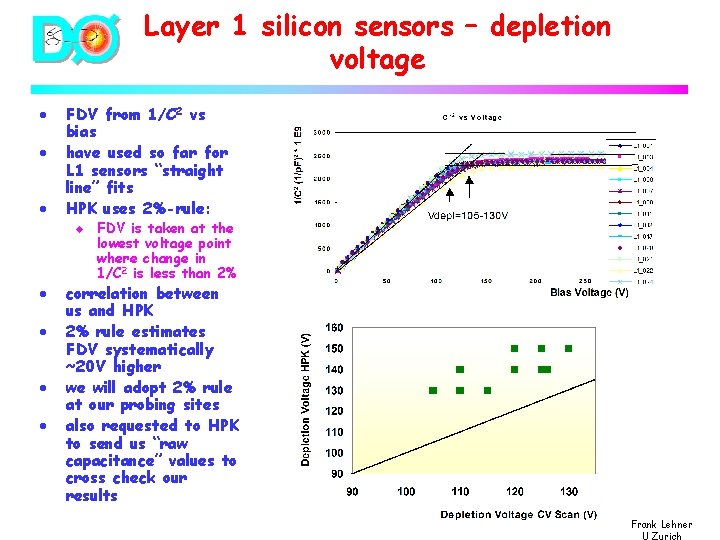
Layer 1 silicon sensors – depletion voltage · · · FDV from 1/C 2 vs bias have used so far for L 1 sensors “straight line” fits HPK uses 2%-rule: u · · FDV is taken at the lowest voltage point where change in 1/C 2 is less than 2% correlation between us and HPK 2% rule estimates FDV systematically ~20 V higher we will adopt 2% rule at our probing sites also requested to HPK to send us “raw capacitance” values to cross check our results Frank Lehner U Zurich

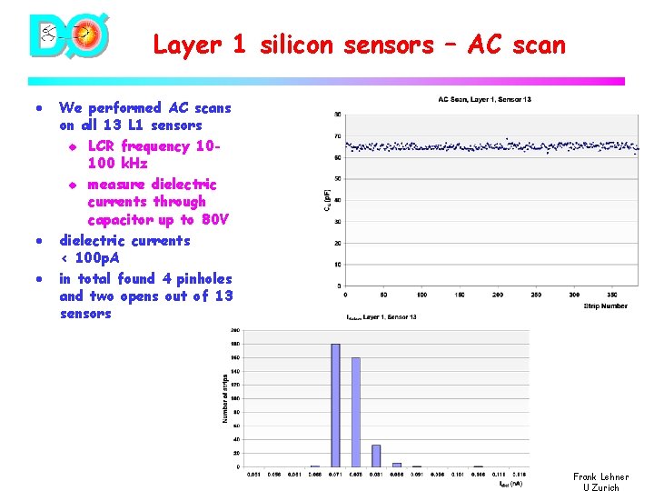
Layer 1 silicon sensors – AC scan · · · We performed AC scans on all 13 L 1 sensors u LCR frequency 10100 k. Hz u measure dielectric currents through capacitor up to 80 V dielectric currents < 100 p. A in total found 4 pinholes and two opens out of 13 sensors Frank Lehner U Zurich

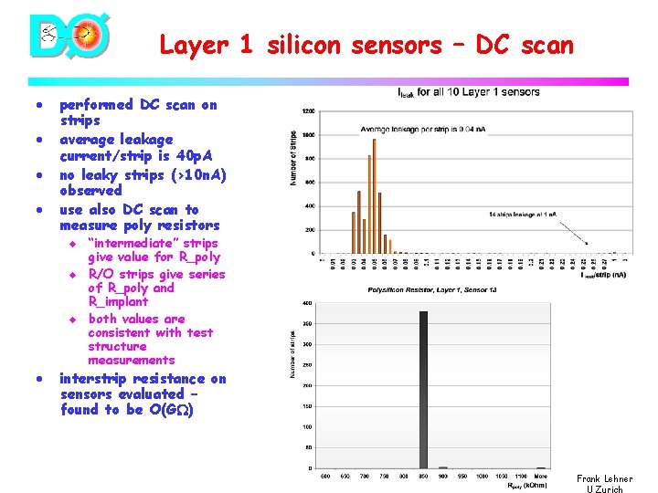
Layer 1 silicon sensors – DC scan · · performed DC scan on strips average leakage current/strip is 40 p. A no leaky strips (>10 n. A) observed use also DC scan to measure poly resistors u u u · “intermediate” strips give value for R_poly R/O strips give series of R_poly and R_implant both values are consistent with test structure measurements interstrip resistance on sensors evaluated – found to be O(G ) Frank Lehner U Zurich

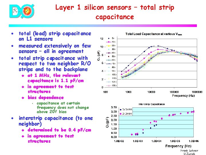
Layer 1 silicon sensors – total strip capacitance · · · total (load) strip capacitance on L 1 sensors measured extensively on few sensors – all in agreement total strip capacitance with respect to two neighbor R/O strips and to the backplane u u u at 1 MHz, the relevant capacitance is 1. 1 p. F/cm in agreement to test structures bias dependence s · capacitance at certain frequency does not change above 20 V bias interstrip capacitance (to one neighbor) u u determined to be 0. 4 p. F/cm in agreement to test structures Frank Lehner U Zurich

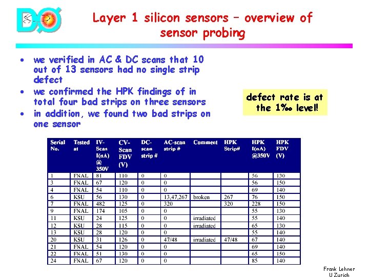
Layer 1 silicon sensors – overview of sensor probing · · · we verified in AC & DC scans that 10 out of 13 sensors had no single strip defect we confirmed the HPK findings of in total four bad strips on three sensors in addition, we found two bad strips on one sensor defect rate is at the 1‰ level! Frank Lehner U Zurich

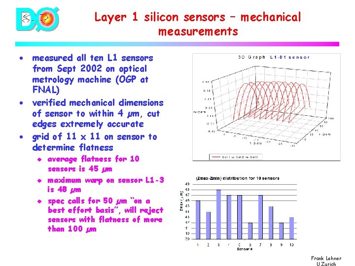
Layer 1 silicon sensors – mechanical measurements · · · measured all ten L 1 sensors from Sept 2002 on optical metrology machine (OGP at FNAL) verified mechanical dimensions of sensor to within 4 µm, cut edges extremely accurate grid of 11 x 11 on sensor to determine flatness u u u average flatness for 10 sensors is 45 µm maximum warp on sensor L 1 -3 is 48 µm spec calls for 50 µm “on a best effort basis”, will reject sensors with flatness of more than 100 µm Frank Lehner U Zurich

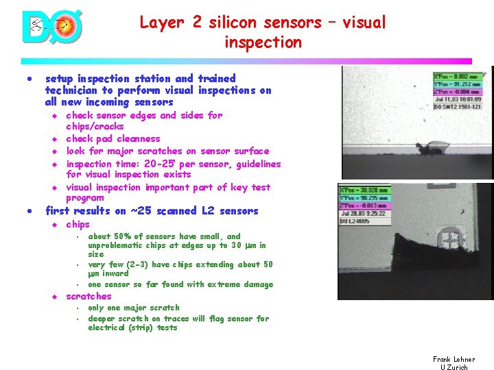
Layer 2 silicon sensors – visual inspection · setup inspection station and trained technician to perform visual inspections on all new incoming sensors u u u · check sensor edges and sides for chips/cracks check pad cleanness look for major scratches on sensor surface inspection time: 20 -25’ per sensor, guidelines for visual inspection exists visual inspection important part of key test program first results on ~25 scanned L 2 sensors u chips s u about 50% of sensors have small, and unproblematic chips at edges up to 30 m in size very few (2 -3) have chips extending about 50 m inward one sensor so far found with extreme damage scratches s s only one major scratch deeper scratch on traces will flag sensor for electrical (strip) tests Frank Lehner U Zurich

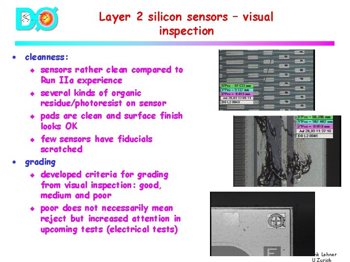
Layer 2 silicon sensors – visual inspection · · cleanness: u sensors rather clean compared to Run IIa experience u several kinds of organic residue/photoresist on sensor u pads are clean and surface finish looks OK u few sensors have fiducials scratched grading u developed criteria for grading from visual inspection: good, medium and poor u poor does not necessarily mean reject but increased attention in upcoming tests (electrical tests) Frank Lehner U Zurich

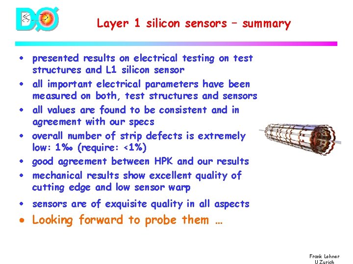
Layer 1 silicon sensors – summary · presented results on electrical testing on test structures and L 1 silicon sensor · all important electrical parameters have been measured on both, test structures and sensors · all values are found to be consistent and in agreement with our specs · overall number of strip defects is extremely low: 1‰ (require: <1%) · good agreement between HPK and our results · mechanical results show excellent quality of cutting edge and low sensor warp · sensors are of exquisite quality in all aspects · Looking forward to probe them … Frank Lehner U Zurich