Characterization of a CMOS cell library for lowvoltage

Characterization of a CMOS cell library for low-voltage operation Department of Electrical and Computer Engineering Jia Yao

Low-power and Low-voltage n n Pavg = Pdyn + Pstatic Pdyn = Ptran + Pshort-circuit Ptran = α * C * Vdd 2 * f Pshort-circuit = Isc * Vdd CMOS: dynamic power Reduction of the power supply voltage is the most efficient way to reduce the power consumption.

Concentration v Study TSMC 0. 18 um standard cell library v Design basic CMOS cells in Hspice and run simulation v Apply supply voltage from high to low to observe the influence of lowering Vdd v Collect data and arrive to conclusion

Basic Parameters n n n The environment temperature : 25 ℃ Input pulse T=24 ns, and the width of input pulse is 12 ns, so the frequency is 41. 6 MHz. Input slew : 0. 03 ns Channel length L=0. 2 um Width Wn=2 um, Wp=2. 4 um Nmos: VTH 0 = 0. 3725327 Pmos: VTH 0 = -0. 3948389
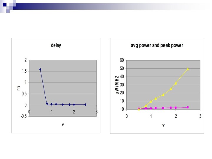
/2 1. Gate Delay ØFor two or more inputs gate,")
Calculation Gate Delay= (tphl+ tplh)/2 1. Gate Delay ØFor two or more inputs gate, calculate delay separately. in Vdd/2 out A Vdd/2 tphl tplh Vdd/2 Y B ØWithout and with outloading Vdd/2 A B Y Y’

Calculation 2. Power Calculation ※ Average power and Peak power ※ For two or more inputs, calculate power separately, keep only one signal changing at one time. ※ Without and with outloading

Inverter 2. 5 v 2. 0 v 1. 8 v 1. 5 v 1. 2 v 1. 0 v 0. 8 v 0. 5 v A→Y↓ (ns) 0. 0092 0. 019 0. 0113 0. 021 0. 0126 0. 023 0. 0151 0. 026 0. 0189 0. 033 0. 0240 0. 042 0. 0377 0. 068 0. 7660 1. 266 A→Y↑ (ns) 0. 015 0. 030 0. 018 0. 036 0. 019 0. 039 0. 023 0. 048 0. 031 0. 065 0. 043 0. 092 0. 081 0. 176 2. 420 5. 036 Delay (ns) 0. 012 0. 025 0. 015 0. 029 0. 016 0. 031 0. 019 0. 037 0. 025 0. 049 0. 034 0. 067 0. 059 0. 122 1. 593 3. 151 Avg Power (u. W/Mhz) 0. 0558 0. 1975 0. 0357 0. 1224 0. 0293 0. 0981 0. 0210 0. 0674 0. 0149 0. 0429 0. 0109 0. 0297 0. 0074 0. 0188 0. 0029 0. 0064 Peak Power 49. 637 76. 98 32. 29 48. 76 25. 32 39. 73 17. 76 26. 83 13. 48 15. 09 9. 71 8. 40 4. 62 3. 23 0. 14 0. 09 0. 0682 0. 489 0. 0519 0. 350 0. 0465 0. 305 0. 0400 0. 248 0. 0371 0. 209 0. 0367 0. 200 0. 0439 0. 299 0. 4714 2. 020 (u. W/Mhz) Power. Delay Product (e-17)

Power-Delay Product

Comparison : with and without outloading Delay Avg Power Peak Power-Delay Product

Nand 2

2. 5 v 2. 0 v 1. 8 v 1. 5 v 1. 2 v 1. 0 v 0. 8 v 0. 5 v A→Y↓ (ns) 0. 016 0. 029 0. 018 0. 033 0. 020 0. 035 0. 023 0. 042 0. 031 0. 055 0. 040 0. 077 0. 083 0. 143 2. 4 2. 987 A→Y↑ (ns) 0. 018 0. 034 0. 021 0. 040 0. 023 0. 044 0. 028 0. 054 0. 038 0. 073 0. 055 0. 104 0. 107 0. 196 3. 280 5. 392 Delay (ns) 0. 017 0. 031 0. 020 0. 036 0. 021 0. 040 0. 026 0. 048 0. 035 0. 064 0. 048 0. 090 0. 095 0. 170 2. 842 4. 190 Avg Power (u. W/Mhz) 0. 0789 0. 2290 0. 0504 0. 1404 0. 0412 0. 1120 0. 0293 0. 0764 0. 0195 0. 0483 0. 0132 0. 0333 0. 0094 0. 0209 0. 0036 0. 0066 Peak Power 48. 25 63. 32 30. 81 38. 17 24. 71 29. 62 17. 66 18. 27 10. 18 9. 08 5. 51 4. 50 1. 90 1. 46 0. 09 0. 11 0. 0134 0. 0719 0. 0099 0. 0511 0. 0088 0. 0445 0. 0075 0. 0364 0. 0068 0. 0310 0. 0063 0. 0301 0. 0089 0. 0354 0. 1029 0. 2760 (u. W/Mhz) Power. Delay Product (e-16)

2. 5 v 2. 0 v 1. 8 v 1. 5 v 1. 2 v 1. 0 v 0. 8 v 0. 5 v B→Y↓ (ns) 0. 019 0. 032 0. 022 0. 036 0. 024 0. 039 0. 029 0. 046 0. 037 0. 061 0. 053 0. 083 0. 096 0. 015 2. 383 3. 762 B→Y↑ (ns) 0. 025 0. 041 0. 030 0. 049 0. 033 0. 054 0. 041 0. 066 0. 058 0. 089 0. 082 0. 125 0. 152 0. 230 3. 989 6. 091 Delay (ns) 0. 022 0. 036 0. 026 0. 043 0. 029 0. 047 0. 035 0. 056 0. 047 0. 075 0. 068 0. 104 0. 122 3. 168 4. 927 Avg Power (u. W/Mhz) 0. 1190 0. 2903 0. 7660 0. 1779 0. 0625 0. 1420 0. 0442 0. 0964 0. 0284 0. 0604 0. 0202 0. 0413 0. 0126 0. 0255 0. 0035 0. 0063 Peak Power 57. 80 64. 08 36. 44 38. 32 28. 99 29. 34 17. 92 18. 02 9. 40 8. 54 6. 04 2. 93 0. 05 0. 0257 0. 105 0. 0198 0. 0756 0. 0178 0. 0664 0. 0155 0. 0543 0. 0134 0. 0454 0. 0136 0. 0429 0. 0156 0. 0312 0. 1115 0. 3108 (u. W/Mhz) Power. Delay Product (e-16)

Comparison : with and without outloading Delay Peak Power Avg Power-Delay Product

NOR 2

2. 5 v 2. 0 v 1. 8 v 1. 5 v 1. 2 v 1. 0 v 0. 8 v 0. 5 v A→Y↓ (ns) 0. 013 0. 022 0. 015 0. 024 0. 016 0. 026 0. 018 0. 029 0. 023 0. 036 0. 029 0. 047 0. 075 1. 005 1. 660 A→Y↑ (ns) 0. 027 0. 06 0. 032 0. 07 0. 037 0. 08 0. 047 0. 100 0. 067 0. 14 0. 011 0. 22 0. 242 0. 45 7. 938 11. 96 Delay (ns) 0. 020 0. 041 0. 024 0. 049 0. 026 0. 053 0. 033 0. 065 0. 045 0. 090 0. 020 0. 131 0. 145 0. 264 4. 471 6. 812 Avg Power (u. W/Mhz) 0. 0775 0. 2298 0. 0500 0. 1399 0. 04098 0. 0294 0. 1108 0. 0745 0. 0189 0. 0465 0. 0139 0. 0319 0. 0091 0. 0201 0. 0034 0. 0054 Peak Power 64. 91 83. 87 42. 72 54. 07 33. 62 43. 32 24. 49 28. 59 16. 20 15. 69 10. 36 8. 62 4. 50 3. 32 0. 12 1. 13 0. 0154 0. 0940 0. 0119 0. 0679 0. 0108 0. 0592 0. 0096 0. 0487 0. 0085 0. 0420 0. 0028 0. 0420 0. 0133 0. 0530 0. 1532 0. 3658 (u. W/Mhz) Power. Delay Product (e-16)

2. 5 v 2. 0 v 1. 8 v 1. 5 v 1. 2 v 1. 0 v 0. 8 v 0. 5 v B→Y↓ (ns) 0. 015 0. 024 0. 017 0. 027 0. 018 0. 021 0. 032 0. 026 0. 040 0. 034 0. 051 0. 055 0. 082 1. 104 1. 762 B→Y↑ (ns) 0. 032 0. 07 0. 040 0. 08 0. 045 0. 09 0. 058 0. 11 0. 083 0. 15 0. 125 0. 22 0. 256 0. 44 7. 141 11. 75 Delay (ns) 0. 024 0. 045 0. 029 0. 053 0. 032 0. 058 0. 039 0. 071 0. 055 0. 096 0. 079 0. 136 0. 155 0. 262 4. 122 0. 6756 Avg Power (u. W/Mhz) 0. 100 0. 0647 0. 2505 0. 1526 0. 0524 0. 1209 0. 0368 0. 0810 0. 0235 0. 0500 0. 0162 0. 0399 0. 0101 0. 0209 0. 0033 0. 0054 Peak Power 70. 48 85. 80 37. 06 42. 85 26. 05 27. 65 15. 04 14. 75 8. 52 7. 93 3. 30 2. 96 0. 05 0. 07 0. 0166 0. 0706 0. 0145 0. 0573 0. 0129 0. 0478 0. 0129 0. 0460 0. 0156 0. 0548 0. 1349 0. 3630 (u. W/Mhz) Power. Delay Product (e-16) 45. 92 54. 08 0. 0240 0. 0186 0. 1124 0. 0812

Comparison : with and without outloading Delay Peak Power Avg Power-Delay Product

Review n Around 1 V n With and without outloading n Separate calculation

Reference 1. Class notes and slides from ELEC 6270 by Dr. Agrawal 2. TSMC 0. 18 um standard cell library data book 3. Hspice user guide 4. Boarh, M. ; Owens, R. M. and Irwin, M. J, “Transistor sizing For low power CMOS circuits’’ IEEE Trans. On Computer. Aided Design of Integrated Circuits and System, vol. 15, pp. 665 -671, 1996
- Slides: 20