
Characterisation of radiationhard Xray sensors for medical applications

- Slides: 14
Characterisation of radiation-hard X-ray sensors for medical applications Filip Segmanovic ESR 15, WP 4 17. 09. 2019
Outline • Introduction • Test-chip design in 180 nm ams technology • Irradiation plan • Measurement methodology • • IV measurements CV measurements • Conclusion and next steps Confidential © ams AG Page 2
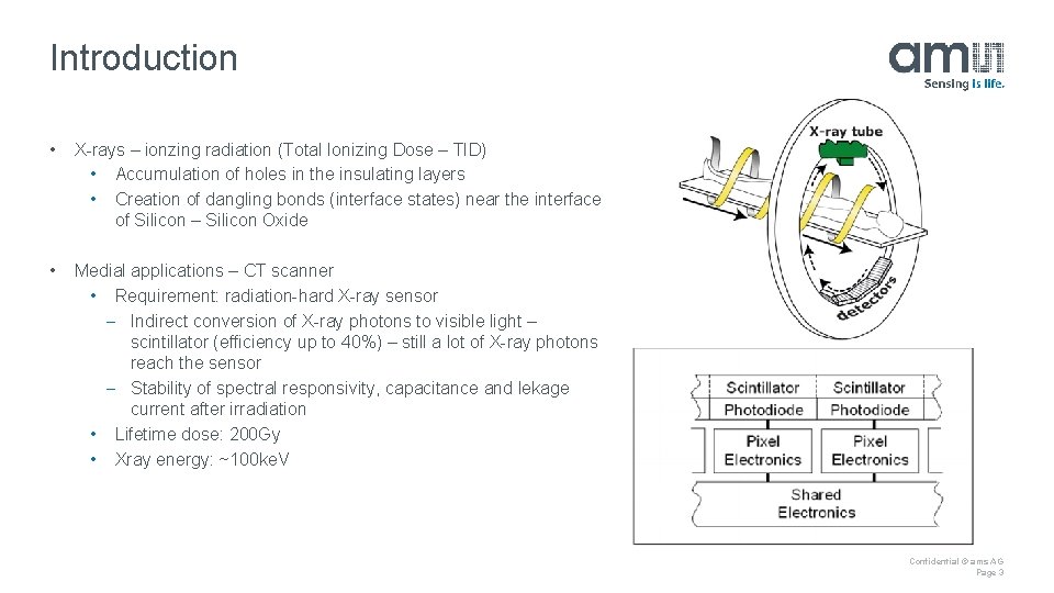
Introduction • X-rays – ionzing radiation (Total Ionizing Dose – TID) • Accumulation of holes in the insulating layers • Creation of dangling bonds (interface states) near the interface of Silicon – Silicon Oxide • Medial applications – CT scanner • Requirement: radiation-hard X-ray sensor - Indirect conversion of X-ray photons to visible light – scintillator (efficiency up to 40%) – still a lot of X-ray photons reach the sensor - Stability of spectral responsivity, capacitance and lekage current after irradiation • Lifetime dose: 200 Gy • Xray energy: ~100 ke. V Confidential © ams AG Page 3
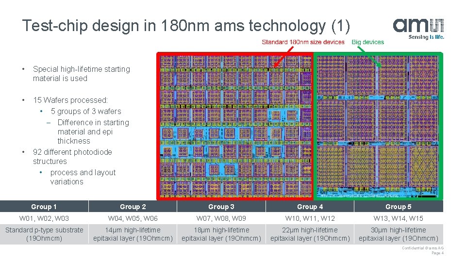
Test-chip design in 180 nm ams technology (1) • Special high-lifetime starting material is used • 15 Wafers processed: • 5 groups of 3 wafers - Difference in starting material and epi thickness 92 different photodiode structures • process and layout variations • Group 1 Group 2 Group 3 Group 4 Group 5 W 01, W 02, W 03 W 04, W 05, W 06 W 07, W 08, W 09 W 10, W 11, W 12 W 13, W 14, W 15 Standard p-type substrate (19 Ohmcm) 14µm high-lifetime epitaxial layer (19 Ohmcm) 18µm high-lifetime epitaxial layer (19 Ohmcm) 22µm high-lifetime epitaxial layer (19 Ohmcm) 30µm high-lifetime epitaxial layer (19 Ohmcm) Confidential © ams AG Page 4
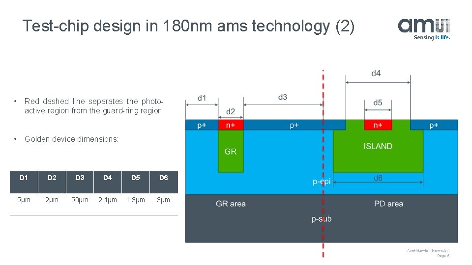
Test-chip design in 180 nm ams technology (2) • Red dashed line separates the photoactive region from the guard-ring region • Golden device dimensions: D 1 D 2 D 3 D 4 D 5 D 6 5µm 2µm 50µm 2. 4µm 1. 3µm Confidential © ams AG Page 5
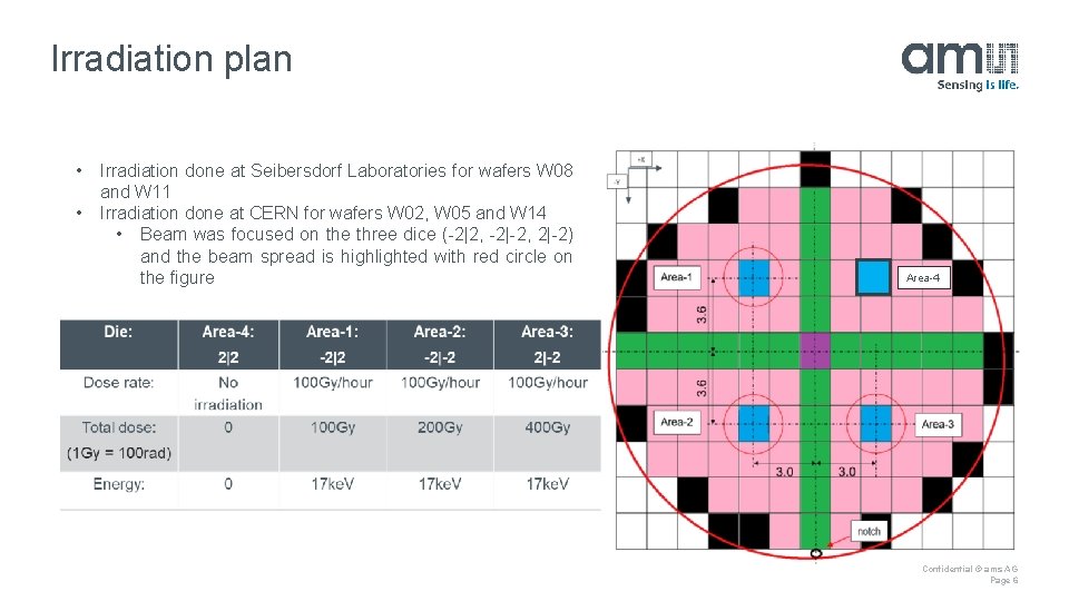
Irradiation plan • • Irradiation done at Seibersdorf Laboratories for wafers W 08 and W 11 Irradiation done at CERN for wafers W 02, W 05 and W 14 • Beam was focused on the three dice (-2|2, -2|-2, 2|-2) and the beam spread is highlighted with red circle on the figure Area-4 Confidential © ams AG Page 6
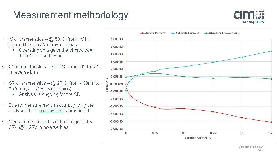
Measurement methodology • IV characteristics – @ 50°C, from 1 V in forward bias to 5 V in reverse bias • Operating voltage of the photodiode: 1. 25 V reverse biased • CV characteristics – @ 27°C, from 0 V to 5 V in reverse bias • SR characteristics – @ 27°C, from 400 nm to 900 nm (@ 1. 25 V reverse bias) • Analysis is ongoing for the SR • Due to measurement inaccuracy, only the analysis of the big devices is presented • Measurement offset is in the range of 1525% @ 1. 25 V in reverse bias Confidential © ams AG Page 7
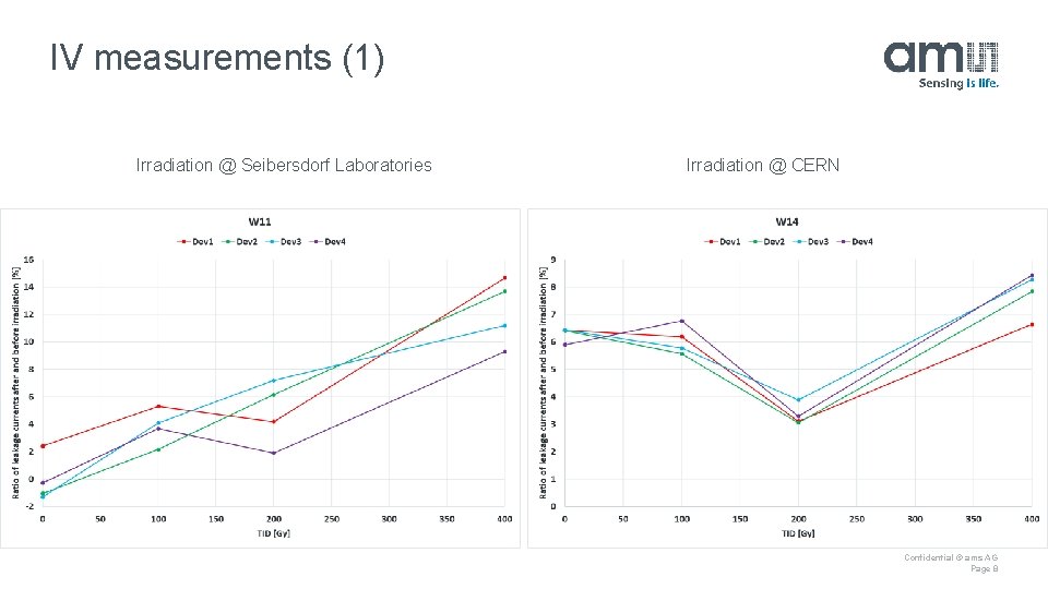
IV measurements (1) Irradiation @ Seibersdorf Laboratories Irradiation @ CERN Confidential © ams AG Page 8
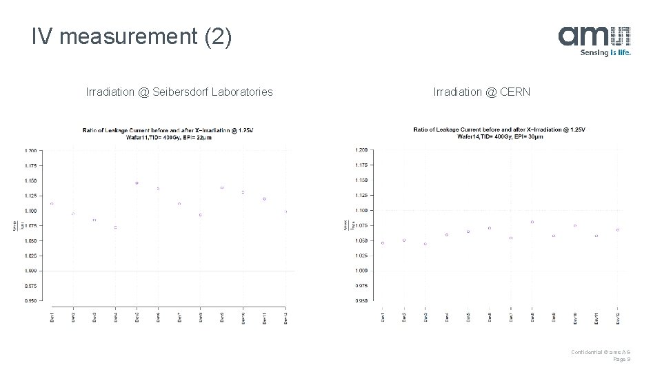
IV measurement (2) Irradiation @ Seibersdorf Laboratories Irradiation @ CERN Confidential © ams AG Page 9
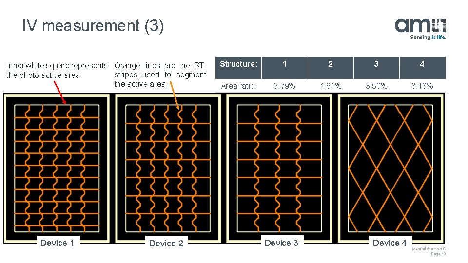
IV measurement (3) Inner white square represents Orange lines are the STI stripes used to segment the photo-active area the active area Device 1 Device 2 Structure: 1 2 3 4 Area ratio: 5. 79% 4. 61% 3. 50% 3. 18% Device 3 Device 4 Confidential © ams AG Page 10
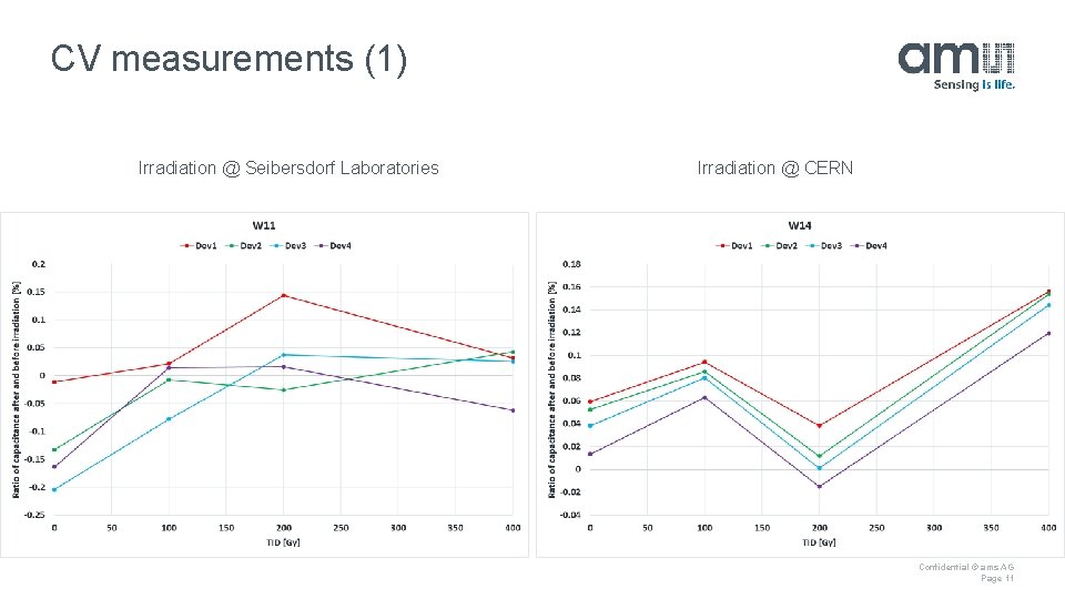
CV measurements (1) Irradiation @ Seibersdorf Laboratories Irradiation @ CERN Confidential © ams AG Page 11
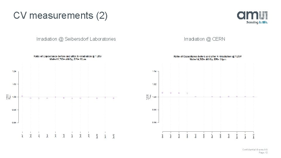
CV measurements (2) Irradiation @ Seibersdorf Laboratories Irradiation @ CERN Confidential © ams AG Page 12
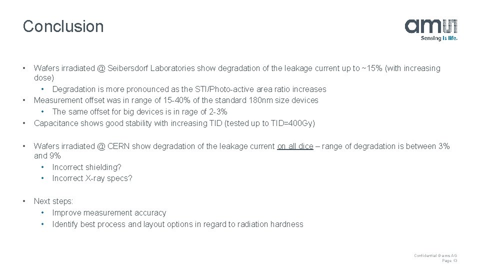
Conclusion • • • Wafers irradiated @ Seibersdorf Laboratories show degradation of the leakage current up to ~15% (with increasing dose) • Degradation is more pronounced as the STI/Photo-active area ratio increases Measurement offset was in range of 15 -40% of the standard 180 nm size devices • The same offset for big devices is in rage of 2 -3% Capacitance shows good stability with increasing TID (tested up to TID=400 Gy) • Wafers irradiated @ CERN show degradation of the leakage current on all dice – range of degradation is between 3% and 9% • Incorrect shielding? • Incorrect X-ray specs? • Next steps: • Improve measurement accuracy • Identify best process and layout options in regard to radiation hardness Confidential © ams AG Page 13
Thank you! Please visit our website www. ams. com