Chapters 3 and 4 Components of Optical Instruments


/4 (l 2 -l 1)/2 l 2 -l")
 0.")


 Number of electrons 1 90 1 2 180 10 3 270 100")


 0. 8 Fe(I) Ni(I) 0. 6 Ni(I) 0. 4 Cr(I) 0.")
 F 2 P(n) Frequency domain P(n) Time domain F 1 P(I) P(n) Frequency")

 P(d) d cm s cm-1 + P(d) P(s) _ d cm + P(d)")
- Slides: 62
Chapters 3 and 4 Components of Optical Instruments
Components of optical instruments Absorption 2. 3. Fluorescence Emission 1. and chemiluminescence phosphorescence Source Wavelength Selector Sample l Rgb back 146, 184. 148 Detector Readout 8888
Construction Materials for Spectroscopic Instruments Wavelength 100 Region VUV 180 UV 380 850 Visible 2000 18000 Near IR IR Li. F Fused silica or quartz Materials for cells, windows, lenses and prisms Corex glass Silica glass Na. Cl KBr Tl. Br or Tl. I Zn. Se 40000 Far IR
Sources for Spectroscopic Instruments Wavelength 100 180 380 Region Sources 850 2000 VAC UV Visible Near IR 18000 IR Ar lamp Xe lamp H 2 or D 2 lamp Tungtstan lamp Continous Nernst glower Zn. O 2+Y 2 O 3 Nichrome wire Glowbar Si. C Line Hollow cathode lamp Lasers 40000 Far IR
Wavelength Selectors for Spectroscopic Instruments Wavelength 100 Region Wavelength selectors VAC 180 380 UV 850 Visible 2000 18000 Near IR IR Far IR Fluorite prism Fused silica or quartz prism Glass prism Continous Na. Cl prism KBr prism 3000 lines/mm Grating 50 lines/mm Interference wedge Discontinous Interference filter Glass filter 40000
Detectors for Spectroscopic Instruments Wavelength 100 180 380 Region Detectors 850 2000 VAC UV Visible Near IR 18000 IR 40000 Far IR Photographic plates Photomultiplier tube Photo tubes Photoelectric Photo cells Photo diodes Charge coupled devices Photo conductors Thermocouples or bolometers Thermal Golay pneumatic cell Pyroelectric cell
Light Amplification by Stimulated Emission of Radiation LASER • Characteristics of a laser: – Spatially narrow and intense – Highly monochromatic – Coherence
Schematic of a Laser Source Nonparallel radiation Active lasing medium Mirror Laser radiation Partially transmitting mirror Radiation Pumping source Power supply
Processes in Laser Action 1 - Pumping Excitation 2 Spontaneous by electrical, emission radiant or chemical energy 3 - Stimulated emission 4 - Absorption Ey’’’ Ey’ Ey Ex Metastable Excited state
Processes in Laser Action 1 - Pumping Excitation 2 Spontaneous by electrical, emission radiant or chemical energy 3 - Stimulated emission 4 - Absorption Ey’’’ Ey’ Ey Ex Metastable Excited state
Light attenuation by absorption Noninverted population Light amplification by stimulated emission Inverted population
E 1 Ey Ey Ex E 0 Three level system Four level system
Conduction band Valence band Conductor Valence band Semiconductor Insulator
p-metal Emitted radiation 3 mm strip width n- type Ga. As substrate n-metal Fig. 7. 9
974 nm laser 450 nm laser Nonlinear crystal Laser diode Fig. 7. 10 Blue-green output
Wavelength Selectors • Filters – Interference – Absorption • Gratings • Prisms
Interference Filters Glass plate Metal film Dielectric layer Metal film Glass plate
Interference Filters q Metal film Dielectric layer t Metal film Condition for reinforcement If q < 10 o nl’ =2 t l= l’h l = 2 th/n nl’ =2 t/cos q
Wedge Type Interference Filters Glass plate Metal film Dielectric layer Metal film Glass plate l 1 l 2
Transmission Characteristic of Interference Filters 100 Effective bandwidth= 15 A Percent Transmittance 80 Effective bandwidth= 15 A 60 40 20 0 5090 Effective bandwidth= 10 A 1/2 Peak height 5110 6215 6225 Wavelength 6940 6960
Effective Bandwidth of Filters 100 Interference Filter Percent Transmittance 80 60 Effective bandwidth=10 nm 40 Absorption Filter 20 Effective bandwidth= 50 nm 0 40 450 500 550
Coupling of Filters 100 Percent Transmittance Orange cut-off filter Green filter 50 Combination of two filters 0 400 500 Wavelength nm 600 700
Czerny Turner Grating Monochromator Concave mirrors Reflection grating Entrance slit Focal plane l 1 l 2 Exit slit
Bunsen Prism Monochromator Entrance slit l 1 Collimating lens Prism Focusing lens l 2 Focal plane Exit slit
Dispersion by a Prism a i r r b Quartz cornu Littrow Mirror
or t c e t De So ur ce Diffracted beams at refelected angle r Monochromatic beams at incident angle i d* sin i + d sin r = l n=1 r d*sin i d*sin r i d
or Diffracted beams at refelected angle r So ur ce ct Dete d*sin i d*sin r d* sin i + d *sin r = 1. 5 * l Monochromatic beams at incident angle i r d*sin i i d*sin r d
Photolithography UV lamp Mask Photoresist Plate Developing solution Etching solution
Performance Characteristics of a Grating Monochromator l + l 1 Exit slit
Dispersion of Monochromators 200 300 400 500 600 700 800 nm Grating 200 350 400 450 500 600 800 nm Glass prism 200 nm 250 300 350 400 500 800 Quartz prism cm 0 5 10 15 20 Distance along focal plane 25
Performance Characteristics of a Grating Monochromator
Echelle Monochromator i r r = i = b = 63 o 26’
, gth nm n e vel a W Echelle grating Diffraction order, n 30 Degree prism 260 Diffraction order, n Prism dispersion 108 300 98 88 400 68 48 620 380 500 600 220 280 340 78 58 240 360 480 560 260 300 280 340 320 460 540 420 500 800 480 760 740 720 700 680 660 640 Wavelength, nm Grating dispersion
Illumination of an Exit Slit l 3 l 1 l 2 Power Monochromator Exit slit l 3 l 2 Wavelength l 1 Detector
Power Slit width= 3(l 2 -l 1)/4 (l 2 -l 1)/2 l 2 -l 1 Effective bandwidth l 3 l 2 Wavelength l 1
Effect of Spectral Bandwidth 0. 700 0. 5 nm bandwidth Wavelength, nm (a) 0. 100 275 0. 100 1. 0 nm bandwidth 220 275 Wavelength, nm (b) 0. 600 Absorbance 0. 100 220 Absorbance 0. 600 2. 0 nm bandwidth 220 275 Wavelength, nm (c)
Characteristics of Radiation Transducers 1. High sensitivity 2. High signal to noise ratio Noise 3. Constant response over considerable range of wavelength 4. Fast response time 5. Zero output signal in the absence of illumination Response Signal Power Higher S/N Wavelength Time Power Response 6. The electrical signal would be directly proportional to radiant power S = k. P+kd Lower S/N Power
Types of Radiation Transducers • Photon transducers – UV, Vis, near IR • Heat transducers – IR, far IR
Response of Detectors 1015 Photomultiplier tube Spectral response. 1014 1013 Cd. S photoconductivity cell 1012 Ga. As photovoltaic cell Cd. Se photoconductivity cell Pb. S photoconductivity cell silicon photodiode 1011 1010 109 Se/Se. O photovoltaic cell Thermocouple 200 600 1000 1400 Wavelength nm 1800 Golay 2200
Photon Transducers • • • Photovoltaic Phototube Photomultiplier tubes Photoconductivity transducers Silicon photodiodes Charge-coupled device
Barrier Layer Cell Glass Thin layer of silver Selenium Plastic case Iron + -
Characteristics of Photovoltaic Cells • • Cell current = 10 – 100 m. A No external electrical energy required. Usually used for low level signals. Low internal resistance = amplification not convenient • Fatigue • Low cost
Photoelectric Effect V
Cathode Wire anode 90 Vdc
Sensitivity, m. A/w Response of some Photoemissive Surfaces 80 K/Cs/Sb 60 40 20 200 Ga/As Ag/O/Cs 400 600 800 Wavelength, nm 1000
Dynode Potential(V) Number of electrons 1 90 1 2 180 10 3 270 100 4 360 103 5 450 104 9 6 540 105 Quartz envelope 7 630 106 8 720 107 810 900 V 108 Gain =108 5 7 3 6 4 2 1 8 Anode Grill Photoemissive Cathode 9 Anode 900 V dc Photoemissive Cathode Dynodes 1 -9 Anode + _ To readout
Features of Photomplier Tubes • High sensitivity in UV, Vis, and NIR – Limited by dark current – Cooling to -30 o. C improves response • Extremely fast time response • Limited to measuring low-level signals
Silicon Diode pn junction Metal contact Lead wire p region n region Fig. 7. 30
Silicon diode under Revese Bias Reverse bias Depletion layer
Silicon Diode under Forward Bias Forward bias e e
Reset Start … 10 -Bit shift register Clock + _ … -5 V … Diode number Spectrum Diode number 1 2 … 1024
Start Pulse Clock Pulse 10 -Bit shift register. Photodiode Array Start Clock FET switch Photodiodec onducts Capacitor dischages + _ FETintegrating switch The closes and the capacitor is integrating charged capacitor proportionaly dischages Integrating An output amplfier proportional to the charge is generated. -5 V FET switch closes Diode number Photodiode Diode No. 1 Ohter capacitor The capacitor is charged to charge up charges up value the original 10 p. F Capacitor 2 1024 Read: Irradiation: A start pulse initializes the shift register Charging: Shutter is opened and the and clock pulses sequentially close FET After a start pulse the shift spectrum is focused switches. This charges up on the capacitors At this stage the PDA isthe ready register sequentially closes PAD. thatthe some diodes and into turn charges integrating start. Note the cycle again. FET switches momentarily receive more photons and capacitor proportionaly. The output to charge up the capacitors less. proportional to charge data issome a voltage of the capacitor.
- No. of charges 5 V + - 10 V + - V 12 Electrodes Si. O 2 Insulator n- doped silicon Substrate
Three phase f 1 f 2 clock output f 3 Optical input Metallic electrodes Potential well p type silicon Insulator Si. O 2
Spectrophotometer slit +15 V Thermocouple junction + _ Reference junction To amplifier + _ -15 V
Light path Coating with refractive index n 2 Fiber with refractive index n 1 Refractive index of medium n 3 Numerical aperture=n 3. sinq=sqrt(n 12+n 22) n 1>n 2>n 3 Fig 7. 37
Optical fibers of different lengths 4 Dye laser 5 3 3 × 3 star coupler 6 Monochromator and detection system 2 1 Fluorescence signals Laser excitation Sample 1 Sample 2 Sample 3
1. 0 Fe(I) 0. 8 Fe(I) Ni(I) 0. 6 Ni(I) 0. 4 Cr(I) 0. 2 Cr(II) 0 33250 Fe(I) Fe(II) 33275 Cr(I) Cr(II) 33300 Wavenumber cm-1 Fig. 7. 39 Fe(I) 33325 33350
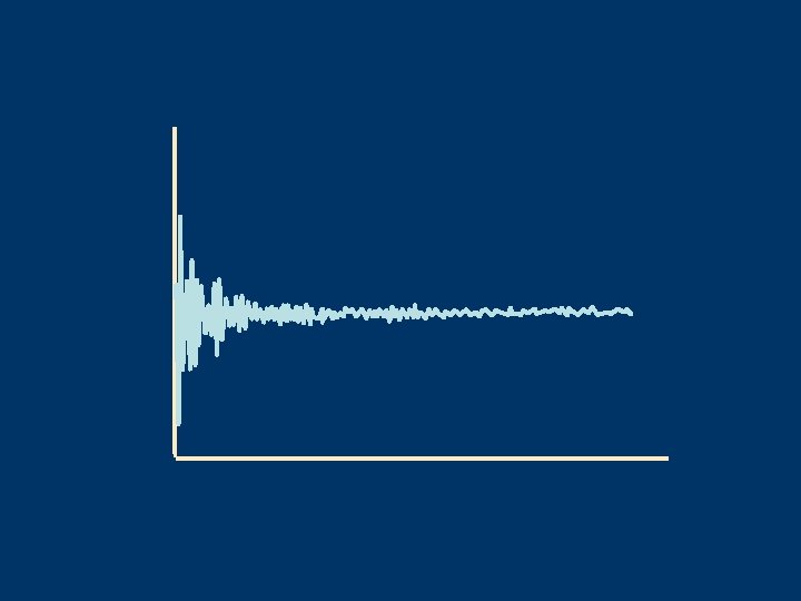
P(I) F 2 P(n) Frequency domain P(n) Time domain F 1 P(I) P(n) Frequency Fig. 7. 40 F 1 F 2
Movable mirror Beam splitting mirror Source -1 l Fixed Mirror Detector 1 2 3
P(s) P(d) d cm s cm-1 + P(d) P(s) _ d cm + P(d) P(s) _ s cm-1 _ d cm + s cm-1