CHAPTER3 Rectifier Filter And Regulator Visit for more


 voltage or current")


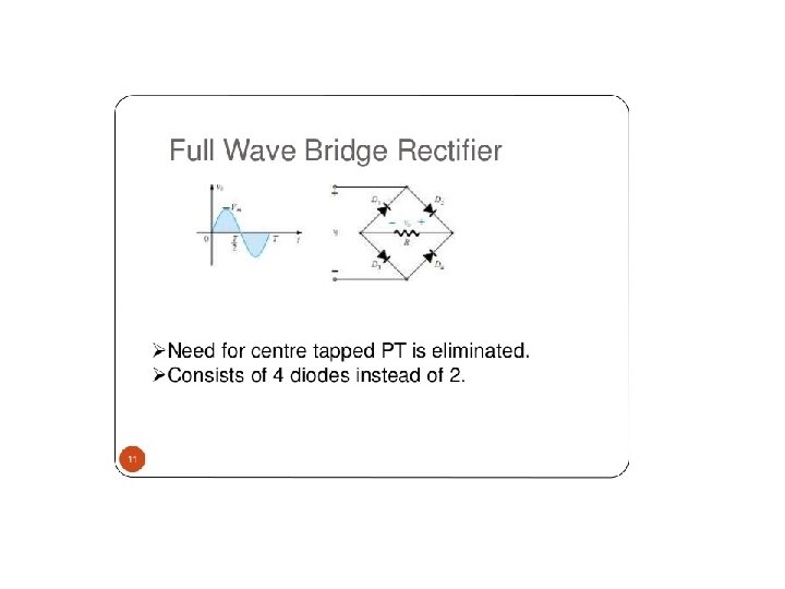
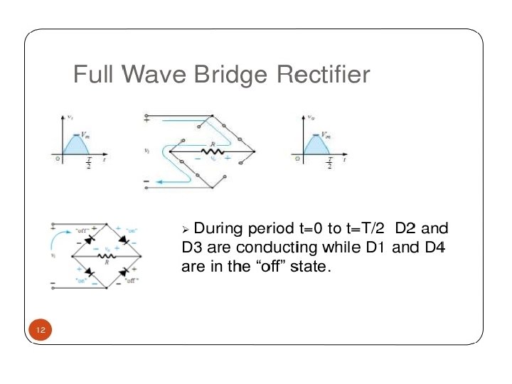
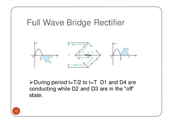
 In this circuit four diodes are used which form a bridge, an")


 filter on shunt capacitor (C) filter")


- Slides: 24
CHAPTER-3 Rectifier Filter And Regulator Visit for more Learning Resources
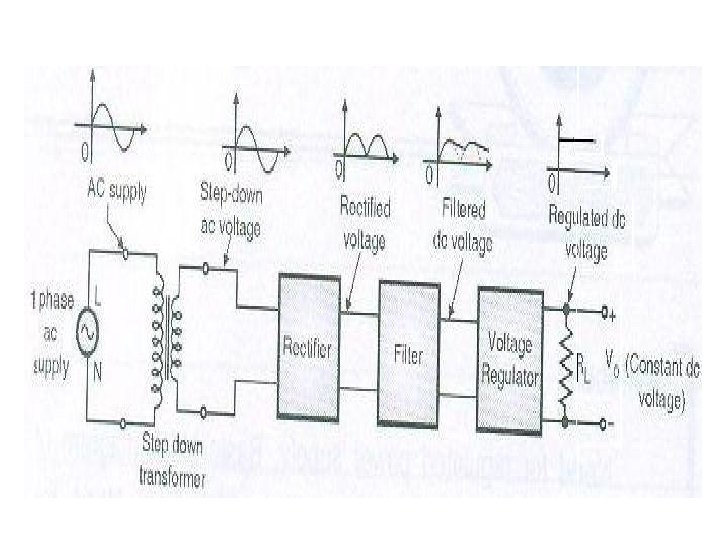
Block diagram of regulated power supply and state its need.
Need of regulated power supply • The unregulated D. C. power supply suffers from the disadvantages of poor voltage regulation and high ripple factor. • This may result the erratic operation of most of the electronic devices and circuits and also electronic gadgets such as pocket radios, electronic calculators, digital watches/ clocks, tape recorders etc. • In order to avoid erratic operations of electronic circuits and also to improve voltage regulation and ripple factor, there is necessity of regulated D. C. power supply.
• Rectifier Def-Rectifier the circuit in which convert the alternating(AC) voltage or current into unidirectional direct(DC) voltage or current. • Types of rectifier circuits 1. HWR(half wave rectifier) 2. FWR(full wave rectifier) with center tapped transformer. 3. FWR with bridge rectifier.
half wave rectifier with shunt capacitor filter. Circuit diagram of half wave rectifier with shunt capacitor filter
Bridge type full wave rectifier.
Working: 1) In this circuit four diodes are used which form a bridge, an ordinary transformer is used. 2) In the +ve half cycle D 1, D 4 hence current flows through D 1, RL and D 4. 3) In the –ve half cycle D 2, D 3 hence current flows through D 1, RL and D 4. 4) In both the cases current passes through the load resistor in the same direction.
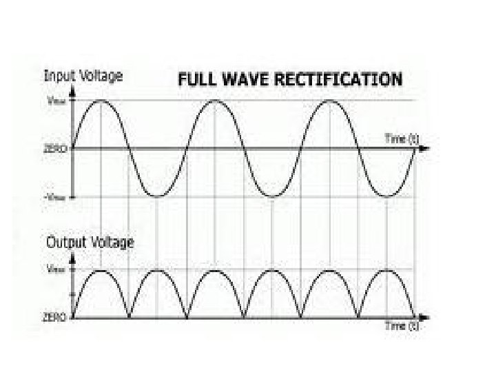
Input and Output waveforms
The types of filter. Filters are classified depending on the components used and depending on the configuration in which they are connected. Some of the important types are as follows: 1. Capacitor input filter (shunt capacitor filter) 2. Choke input filter (series inductor filter) 3. LC filter 4. π type filter OR CLC filter 5. RC filter.
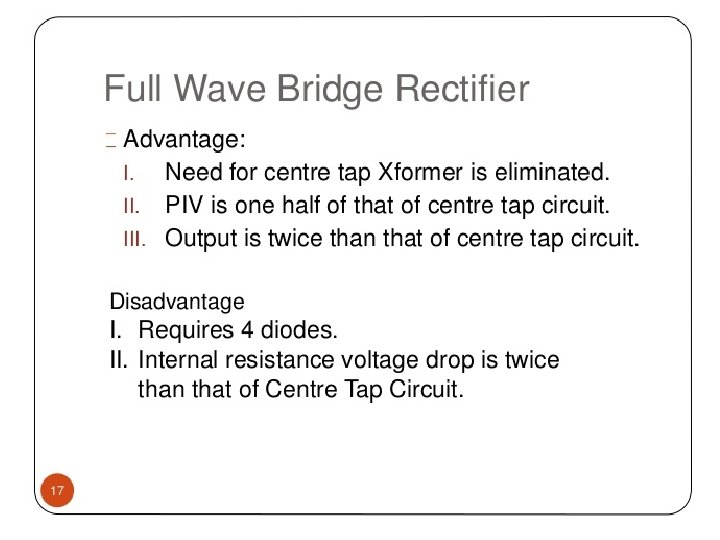
Differentiate between Half wave rectifier and bridge full wave rectifier Parameters Half Wave Bridge Full Wave 1 Number of diodes 1 4 2 Peak secondary voltage, Vs Vm Vm 3 Peak Inverse voltage Vm Vm 4 D. C. current ID. C Im/ π =0. 318 Im 2 Im/ π =0. 636 Im 5 Maximum rectification efficiency, 6 ηmax 40. 6% 81. 2% 6 Transformer utilization factor(TUF) 0. 287 0. 812 7 Ripple frequency, fr fi 2 fi
Advantages of centre tapped full wave rectifier over half wave rectifier 1. The DC output voltage and load current values of full wave rectifier are twice than those of half wave rectifier. 2. The ripple factor is much less (0. 482) than that of half wave rectifier (1. 21). 3. The efficiency of full wave rectifier is twice (81. 2%) than that of half wave rectifier (40. 6%). 4. The TUF of full wave rectifier is more than that of half wave rectifier.
LC filter.
Working • The combination of series inductor (L) filter on shunt capacitor (C) filter is known as LC filter. • This filter is also known as the rectifier is applied across the input terminals of the choke input filter. • The pulsating output of the rectifier contains AC as well as DC component of current. The choke L passes the DC component from the rectifier because its DC resistance R is very small. • It opposes the AC component capacitor C bypasses AC component that presents at the output of inductor L but prevents DC component to flow through it. • Therefore only DC component reaches to the load resistor RL.
The need of rectification. 1. Every electronic circuit such as amplifiers needs a dc power source for its operation. 2. This dc voltage has to be obtained from the ac supply. 3. For this the ac supply has to be reduced (stepped down) first using a step down transformer and then converted to dc by using rectifier.
The circuit diagram of CLC filter.
EX Following figure shows a centre tapped full wave rectifier circuit. Assuming both diodes to be ideal determine: 1. DC output voltage (Vdc) 2. Peak Inverse Voltage (PIV) of diode
Given: V 1 = 230 V 1. We know that the secondary voltage V 2 =N 2/N 1 x V 1 = 230 x 1/5 = 46 volts Maximum value of secondary voltage Vm = √ 2 x V 2 = √ 2 x 46 = 65. 05 volts Therefore, DC voltage Vdc=Vm/π=65. 04/3. 14=20. 71 V 2. PIV of Diode = Vm = 65. 05 volts.
An A. C. supply of 230 V is applied to half wave rectifier circuit through a transformer of turns ratio 2: 1 Calculate i. DC output voltage ii. PIV of diode Given: V 1= 230 V N 2/N 1 = 1/ 2 1. We know that secondary voltage 2. V 2 = N 2/N 1 x V 1 = 230 x 1/ 2 = 115 V Maximum value of secondary voltage Vm= √ x V 2 = √ x 115 V = 162. 6 volts Therefore, DC voltage Vdc= Vm /π = 162. 6/ 3. 14 = 51. 7 volts 2. PIV of diode = Vm= 162. 6 volts For more detail contact us