CHAPTER 9 MULTIPLEXERS DECODERS AND PROGRAMMABLE LOGIC DEVICES
CHAPTER 9 MULTIPLEXERS, DECODERS, AND PROGRAMMABLE LOGIC DEVICES This chapter in the book includes: Objectives Study Guide 9. 1 Introduction 9. 2 Multiplexers 9. 3 Three-State Buffers 9. 4 Decoders and Encoders 9. 5 Read-Only Memories 9. 6 Programmable Logic Devices 9. 7 Complex Programmable Logic Devices 9. 8 Field Programmable Gate Arrays Problems
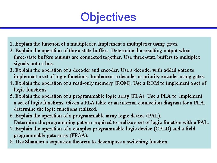
Objectives 1. Explain the function of a multiplexer. Implement a multiplexer using gates. 2. Explain the operation of three-state buffers. Determine the resulting output when three-state buffers outputs are connected together. Use three-state buffers to multiplex signals onto a bus. 3. Explain the operation of a decoder and encoder. Use a decoder with added gates to implement a set of logic functions. Implement a decoder or priority encoder using gates. 4. Explain the operation of a read-only memory (ROM). Use a ROM to implement a set of logic functions. 5. Explain the operation of a programmable logic array (PLA). Use a PLA to implement a set of logic functions. Given a PLA table or an internal connection diagram for a PLA, determine the logic functions realized. 6. Explain the operation of a programmable array logic device (PAL). Determine the programming pattern required to realize a set of logic function with a PAL. 7. Explain the operation of a complex programmable logic device (CPLD) and a field programmable gate array (FPGA). 8. Use Shannon’s expansion theorem to decompose a switching function.
9. 1 Introduction • Multiplexer, Decoder, encoder. Three-state Buffer • ROMs • PLD • PLA • CPLD • FPGA
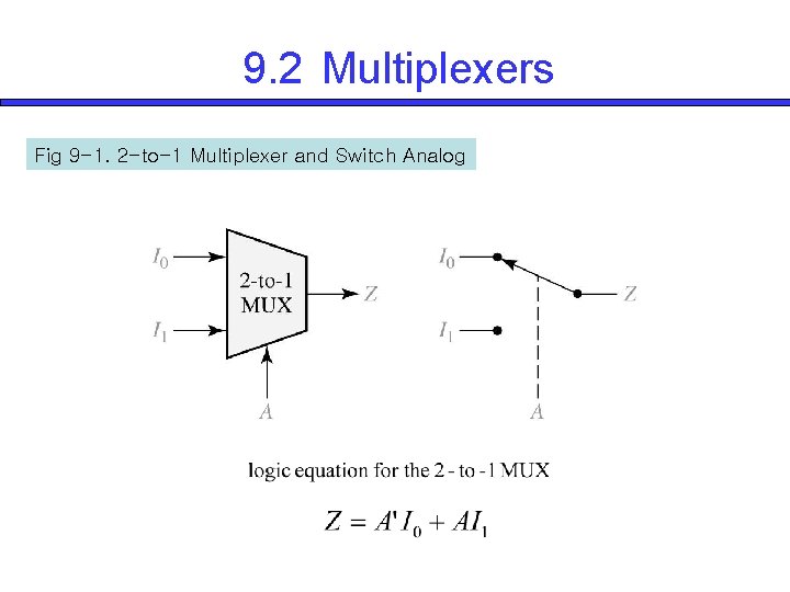
9. 2 Multiplexers Fig 9 -1. 2 -to-1 Multiplexer and Switch Analog
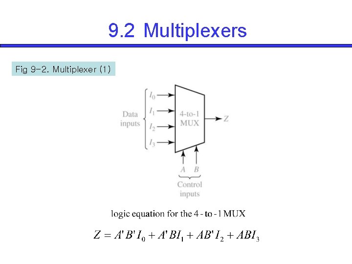
9. 2 Multiplexers Fig 9 -2. Multiplexer (1)
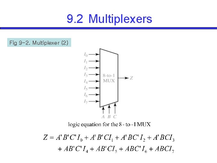
9. 2 Multiplexers Fig 9 -2. Multiplexer (2)
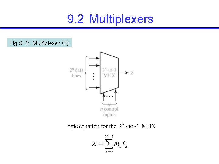
9. 2 Multiplexers Fig 9 -2. Multiplexer (3)
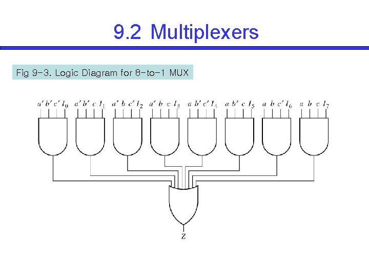
9. 2 Multiplexers Fig 9 -3. Logic Diagram for 8 -to-1 MUX
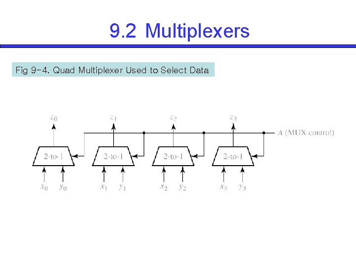
9. 2 Multiplexers Fig 9 -4. Quad Multiplexer Used to Select Data
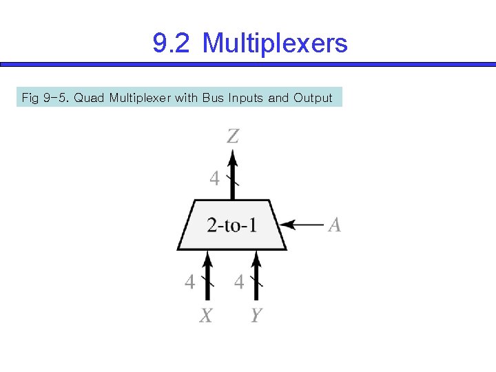
9. 2 Multiplexers Fig 9 -5. Quad Multiplexer with Bus Inputs and Output
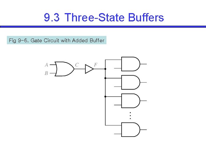
9. 3 Three-State Buffers Fig 9 -6. Gate Circuit with Added Buffer
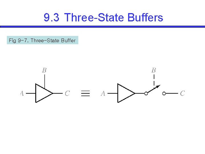
9. 3 Three-State Buffers Fig 9 -7. Three-State Buffer
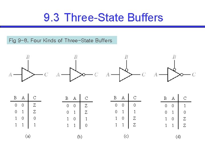
9. 3 Three-State Buffers Fig 9 -8. Four Kinds of Three-State Buffers B A C 0 0 1 1 0 1 Z Z 0 1 0 0 1 1 0 1 Z Z 1 0 0 0 1 1 0 1 0 1 Z Z 0 0 1 1 0 Z Z (a) (b) (c) (d)
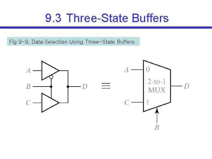
9. 3 Three-State Buffers Fig 9 -9. Data Selection Using Three-State Buffers
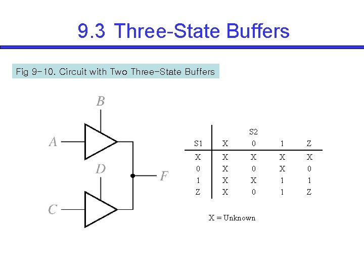
9. 3 Three-State Buffers Fig 9 -10. Circuit with Two Three-State Buffers S 1 X S 2 0 X 0 1 Z X X X 0 X = Unknown 1 Z X X 1 1 X 0 1 Z
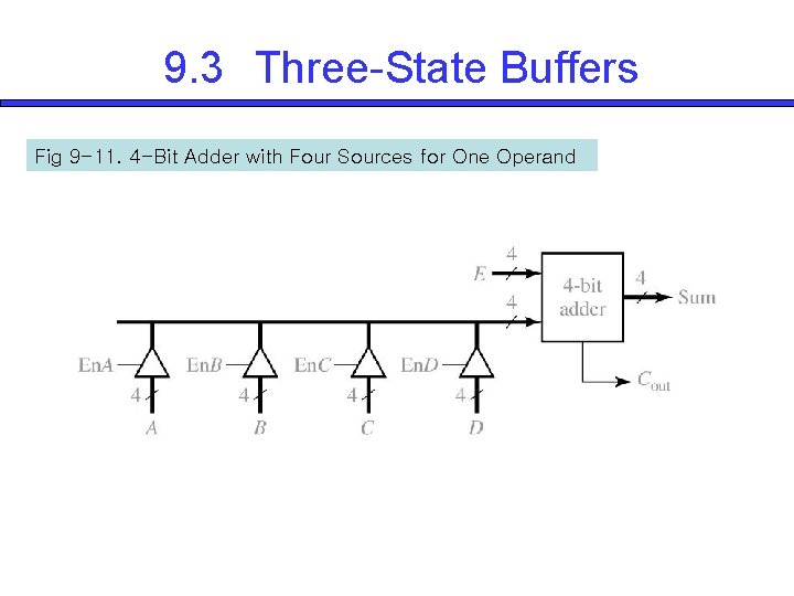
9. 3 Three-State Buffers Fig 9 -11. 4 -Bit Adder with Four Sources for One Operand
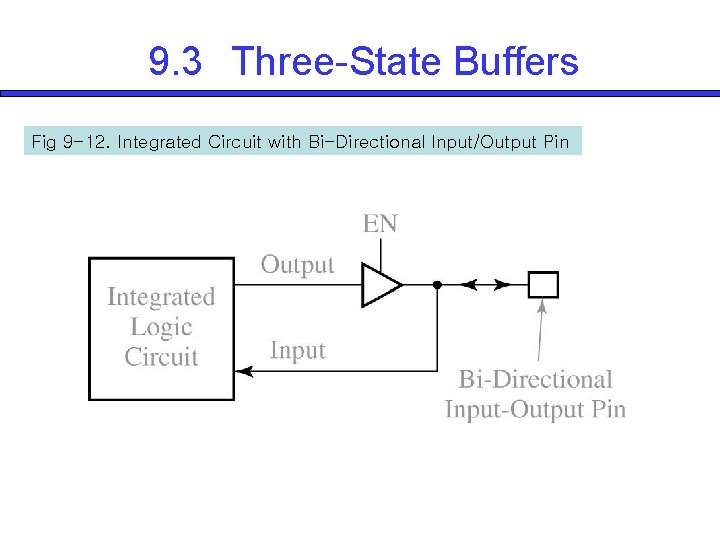
9. 3 Three-State Buffers Fig 9 -12. Integrated Circuit with Bi-Directional Input/Output Pin
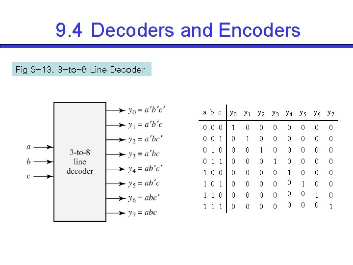
9. 4 Decoders and Encoders Fig 9 -13. 3 -to-8 Line Decoder a b c y 0 y 1 y 2 y 3 y 4 y 5 y 6 y 7 0 0 1 1 1 0 0 0 0 0 1 1 0 1 0 0 0 0 0 0 0 0 1 0 0 0 0 0 1
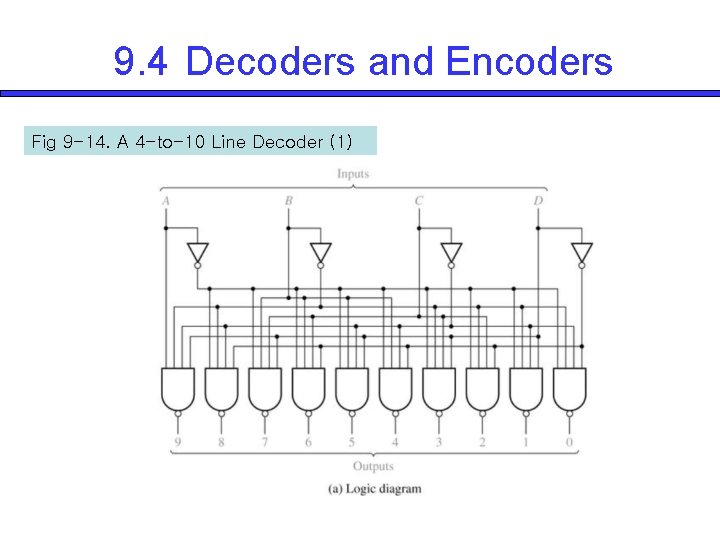
9. 4 Decoders and Encoders Fig 9 -14. A 4 -to-10 Line Decoder (1)
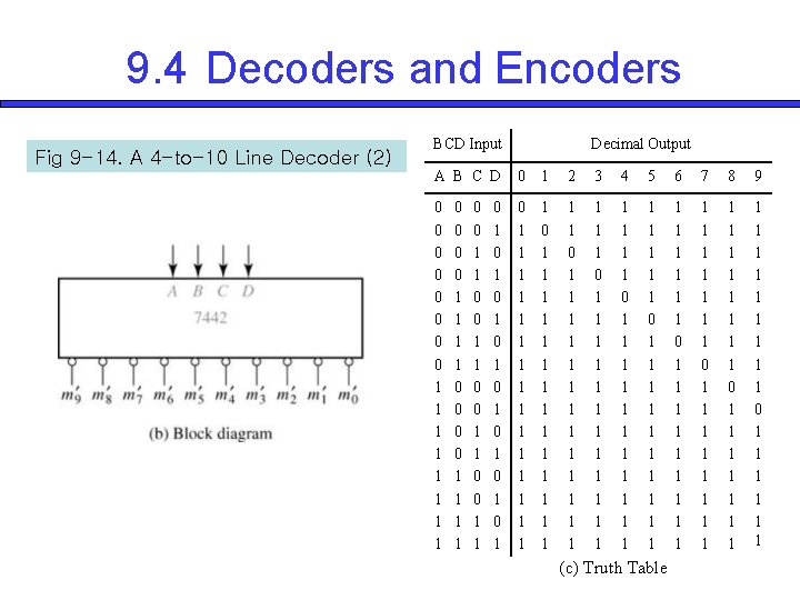
9. 4 Decoders and Encoders Fig 9 -14. A 4 -to-10 Line Decoder (2) BCD Input Decimal Output A B C D 0 1 2 3 4 5 6 7 8 9 0 0 0 0 1 1 1 1 1 1 1 1 1 1 1 1 1 1 1 1 0 1 1 1 1 1 1 1 1 1 1 1 1 1 1 1 1 0 1 1 1 1 1 1 1 1 0 0 0 0 1 1 1 1 0 0 1 1 0 1 0 1 (c) Truth Table
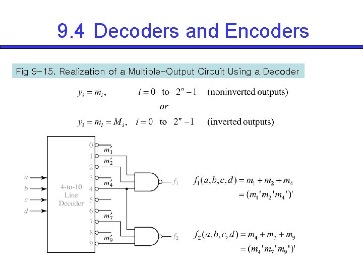
9. 4 Decoders and Encoders Fig 9 -15. Realization of a Multiple-Output Circuit Using a Decoder
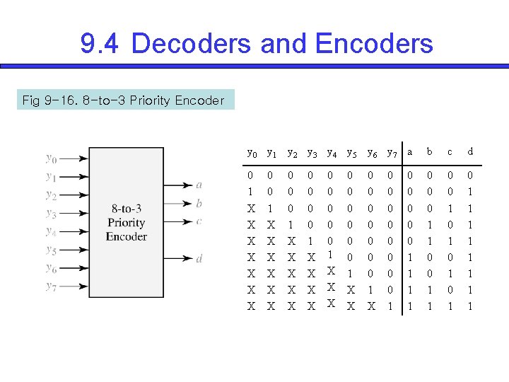
9. 4 Decoders and Encoders Fig 9 -16. 8 -to-3 Priority Encoder y 0 y 1 y 2 y 3 y 4 y 5 y 6 y 7 a b c d 0 1 X X X X 0 0 0 1 1 0 0 1 0 1 0 1 1 1 1 0 0 1 X X X 0 0 1 X X 0 0 0 1 X X 0 0 0 0 1 0 0 0 1 1
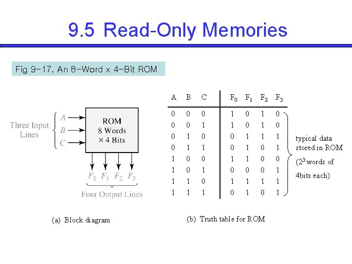
9. 5 Read-Only Memories Fig 9 -17. An 8 -Word x 4 -Bit ROM (a) Block diagram A B C F 0 F 1 F 2 F 3 0 0 1 1 0 1 0 1 1 1 0 0 0 1 1 1 1 1 0 0 0 1 1 1 (b) Truth table for ROM typical data stored in ROM (23 words of 4 bits each)
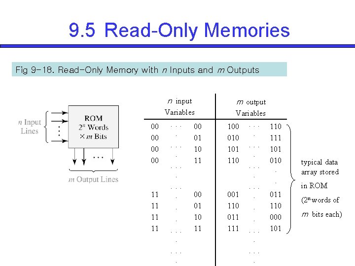
9. 5 Read-Only Memories Fig 9 -18. Read-Only Memory with n Inputs and m Outputs 00 00 11 11 n input m output Variables ··· · · · ··· · 00 01 10 11 100 010 101 110 011 111 ··· · · · ··· · 110 111 101 010 · · 011 110 000 101 typical data array stored in ROM (2 n words of m bits each)
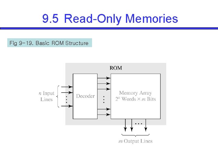
9. 5 Read-Only Memories Fig 9 -19. Basic ROM Structure
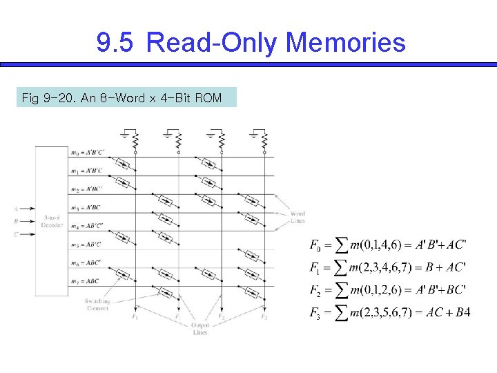
9. 5 Read-Only Memories Fig 9 -20. An 8 -Word x 4 -Bit ROM
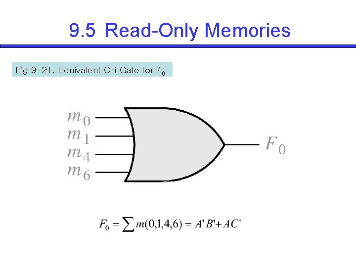
9. 5 Read-Only Memories Fig 9 -21. Equivalent OR Gate for F 0
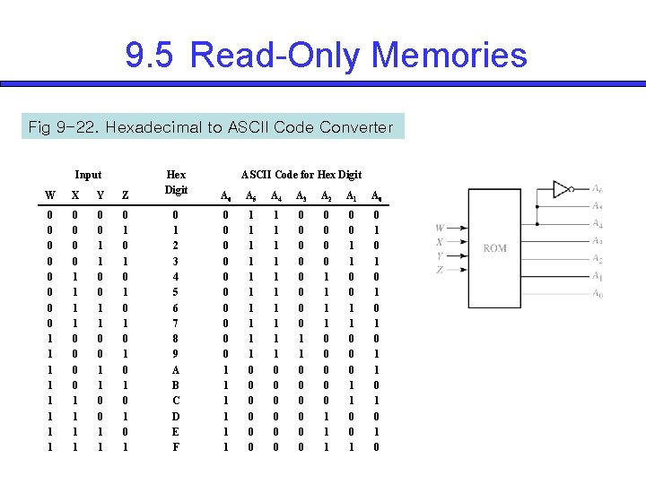
9. 5 Read-Only Memories Fig 9 -22. Hexadecimal to ASCII Code Converter Input W X Y Z Hex Digit 0 0 0 0 1 1 1 1 0 0 1 1 0 1 0 1 0 1 2 3 4 5 6 7 8 9 A B C D E F ASCII Code for Hex Digit A 6 A 5 A 4 A 3 A 2 A 1 A 0 0 0 1 1 1 1 0 0 0 1 1 1 1 1 0 0 0 0 1 1 0 0 0 0 0 1 1 1 0 0 1 1 0 0 1 0 1 0 1 0
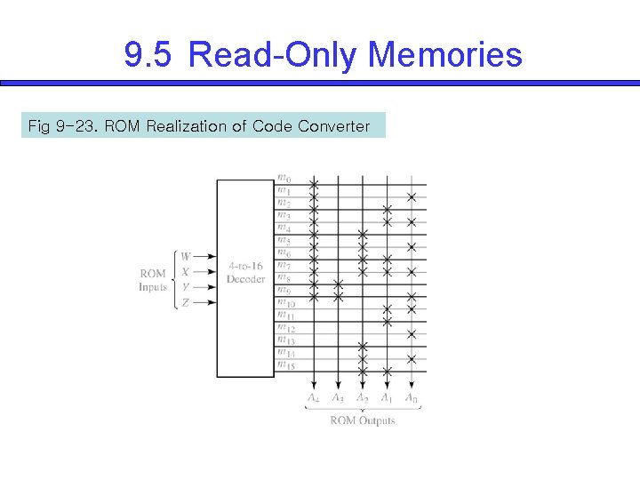
9. 5 Read-Only Memories Fig 9 -23. ROM Realization of Code Converter
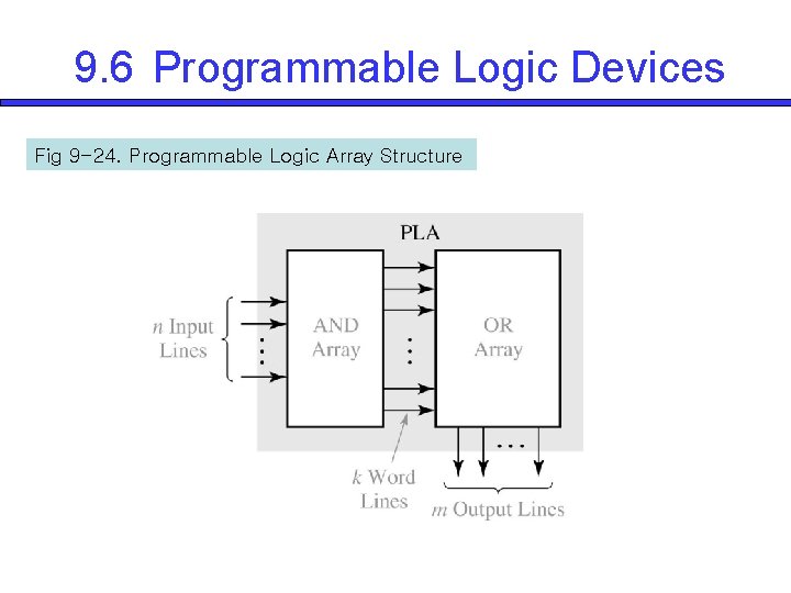
9. 6 Programmable Logic Devices Fig 9 -24. Programmable Logic Array Structure
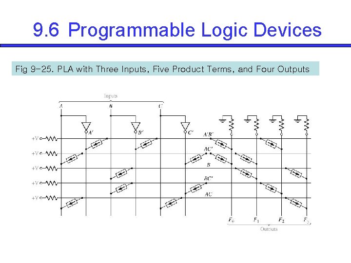
9. 6 Programmable Logic Devices Fig 9 -25. PLA with Three Inputs, Five Product Terms, and Four Outputs
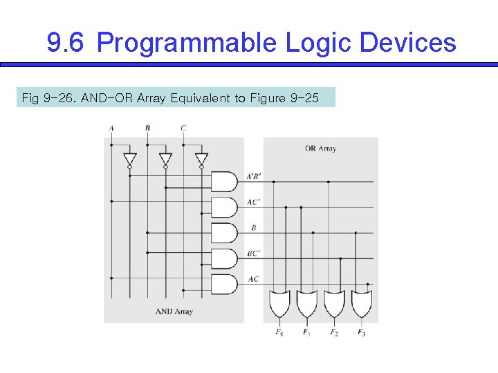
9. 6 Programmable Logic Devices Fig 9 -26. AND-OR Array Equivalent to Figure 9 -25
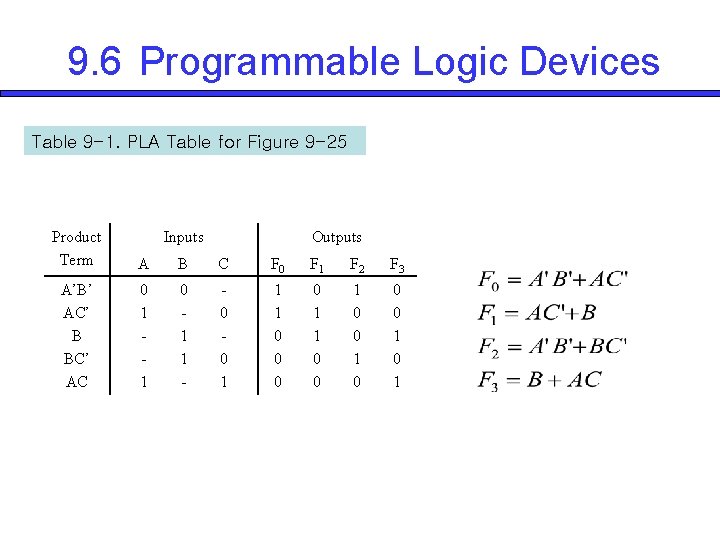
9. 6 Programmable Logic Devices Table 9 -1. PLA Table for Figure 9 -25 Product Term Inputs Outputs A B C F 0 F 1 F 2 F 3 A’B’ AC’ B BC’ AC 0 1 1 - 0 0 1 1 1 0 0 1 0 0 0 1
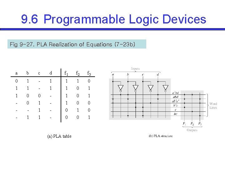
9. 6 Programmable Logic Devices Fig 9 -27. PLA Realization of Equations (7 -23 b) a b c d f 1 f 2 f 3 0 1 1 - 1 1 0 0 1 0 0 1 1 0 0 1 (a) PLA table

9. 6 Programmable Logic Devices Programmable Array Logic The symbol of Figure 9 -28(a) logically equal
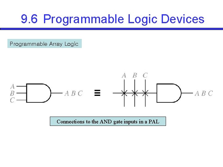
9. 6 Programmable Logic Devices Programmable Array Logic Connections to the AND gate inputs in a PAL
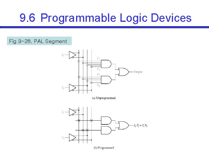
9. 6 Programmable Logic Devices Fig 9 -28. PAL Segment
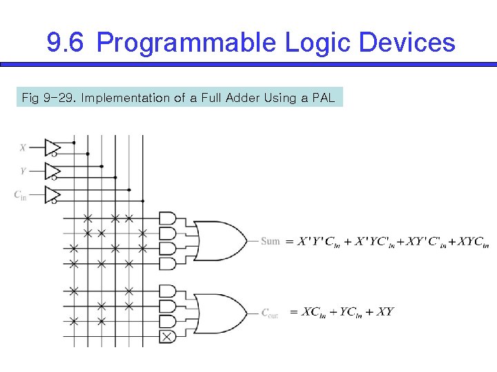
9. 6 Programmable Logic Devices Fig 9 -29. Implementation of a Full Adder Using a PAL
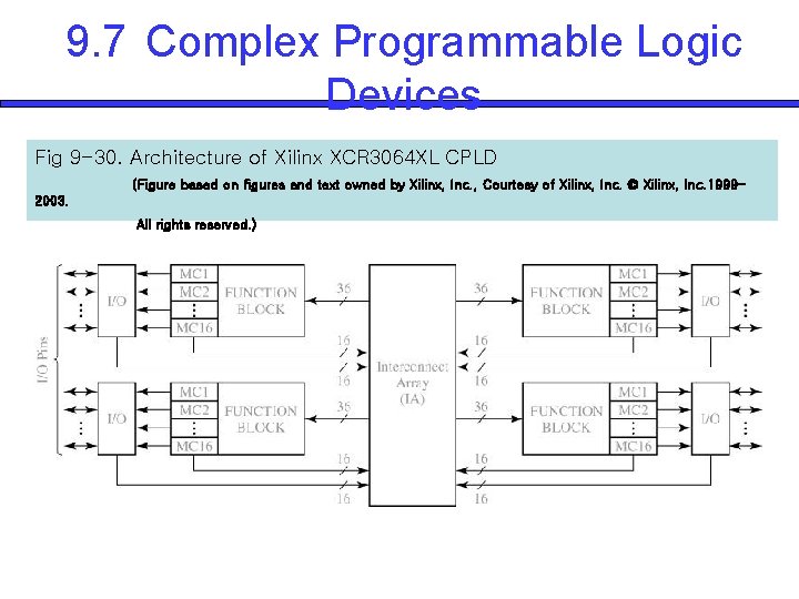
9. 7 Complex Programmable Logic Devices Fig 9 -30. Architecture of Xilinx XCR 3064 XL CPLD (Figure based on figures and text owned by Xilinx, Inc. , Courtesy of Xilinx, Inc. © Xilinx, Inc. 19992003. All rights reserved. )
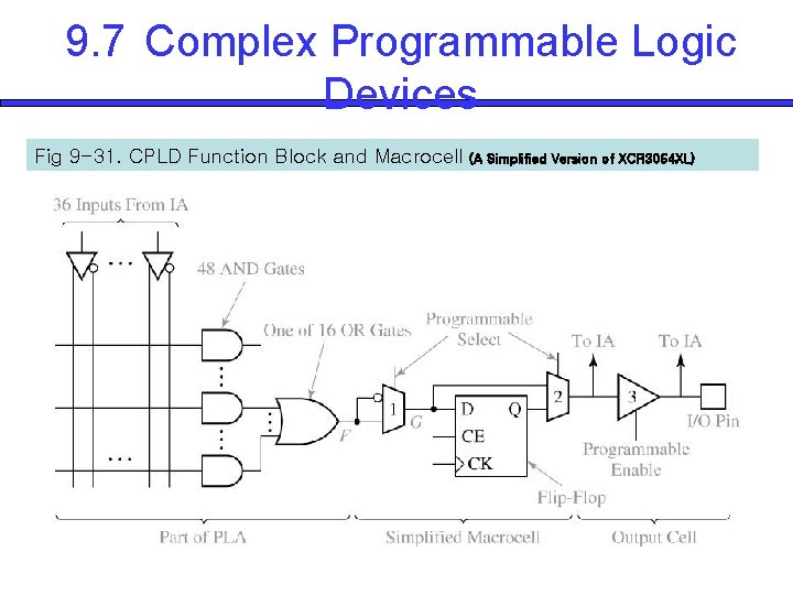
9. 7 Complex Programmable Logic Devices Fig 9 -31. CPLD Function Block and Macrocell (A Simplified Version of XCR 3064 XL)
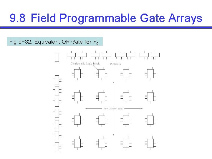
9. 8 Field Programmable Gate Arrays Fig 9 -32. Equivalent OR Gate for F 0
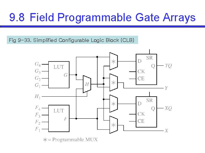
9. 8 Field Programmable Gate Arrays Fig 9 -33. Simplified Configurable Logic Block (CLB)
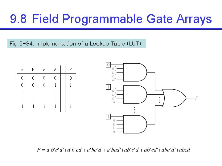
9. 8 Field Programmable Gate Arrays Fig 9 -34. Implementation of a Lookup Table (LUT) a b c d f 0 0 · · 1 0 1 · · 1
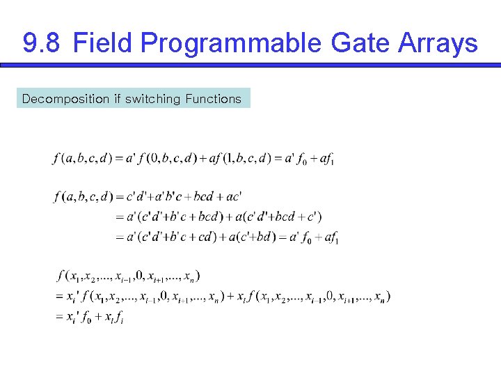
9. 8 Field Programmable Gate Arrays Decomposition if switching Functions
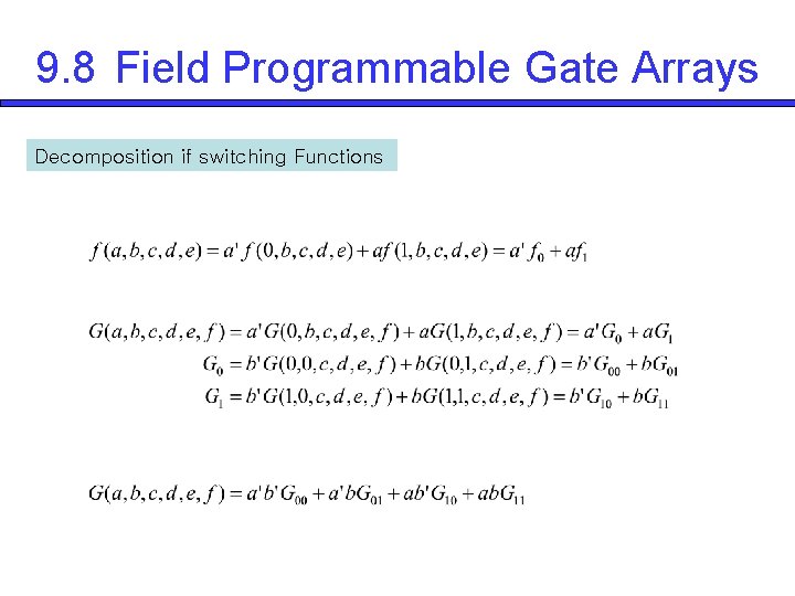
9. 8 Field Programmable Gate Arrays Decomposition if switching Functions
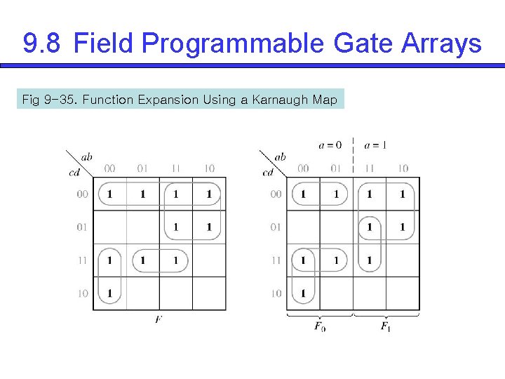
9. 8 Field Programmable Gate Arrays Fig 9 -35. Function Expansion Using a Karnaugh Map
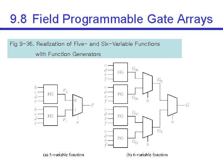
9. 8 Field Programmable Gate Arrays Fig 9 -36. Realization of Five- and Six-Variable Functions with Function Generators
- Slides: 47