Chapter 9 Microcontrollers The Atmel AVR 9 1






- Slides: 43

Chapter 9 Microcontrollers: The Atmel AVR

9. 1 Background ● Microcontroller computer used for smallscaled control operations inside devices that one doesn't usually think of as being computers. Examples ● ● Traffic lights Toasters thermostats Elevators Even in modern automobiles—anti-lock braking, airbags, adjusting fuel mixtures.

9. 1 Background ● Three main characteristics: Embedded systems—running specialized single purpose code as part of a larger system, not general-purpose user-programmable computers. Smaller—less-capable computers Single-chip gadgets—memory and most of their peripheral interfaces located on the same physical chip.

9. 1 Background ● Companies that make and sell microcontrollers: Microchip Intel AMD Motorola Zilog Toshiba Hitachi General Instrumentation

9. 1 Background ● AVR is fairly typical in its capacities, but differs in interesting ways from more mainstream chips such as the Pentium or Power. PC.

9. 2. 1 Central Processing Unit ● AVR uses RISC design principles. Instruction constrained to 16 bits, including arguments. Instruction set tuned specifically for the usual needs of a microcontroller large number of bit instructions for the manipulation of individual electrical signals. Only about 130 different instructions (fewer than there are on the JVM). 32 general purpose registers, 64 so-called I/O registers, 8 bits wide Register can be used in pairs to permit larger numbers to be accessed

9. 2. 1 Central Processing Unit No support for floating point numbers. ALU will only do operations on integer types. Special-purpose instruction register, program counter, stack pointer.

9. 2. 2 Memory ● Three separate memory banks differ physically and in their size and capacities. Memory capacity differs from model to model. Harvard architecture design ● Different physical storage banks (and different data buses) are available for transferring machine instructions and data. They can each be independently tuned to maximize performance. The computer can load instructions and data at the same time, an effective doubling of speed.

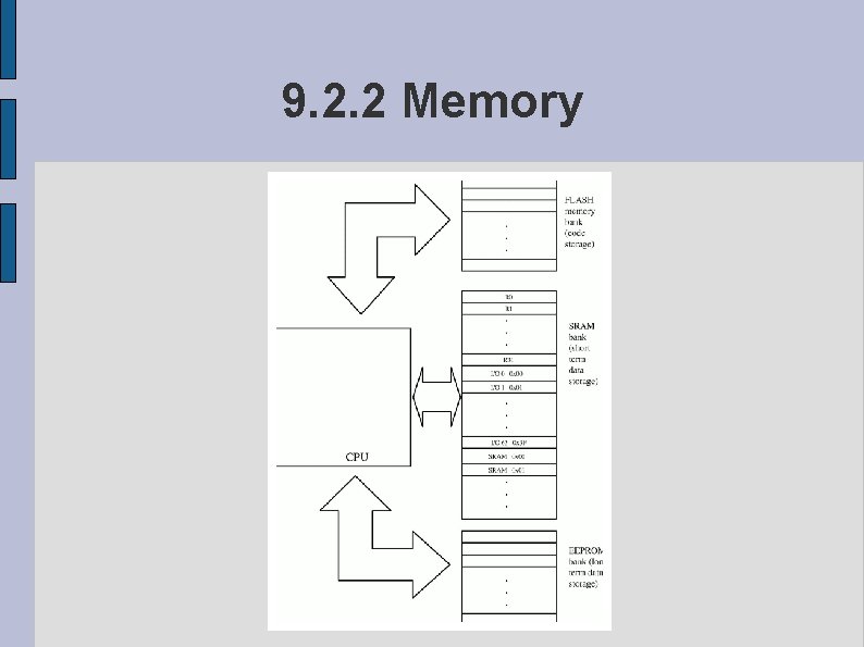
9. 2. 2 Memory

9. 2. 2 Memory ● AVR's three separate banks of memory: Read-only bank used for program code. Read/write bank of high speed memory for program variables. Long-term storage of program data that must survive a power outage.

9. 2. 2 Memory ● ROM and RAM Distinction is more fundamental in theory than it has become in practice. In practical terms the modern definition of the ROM/RAM distinction is a difference in use; whether or not the CPU is intended to be able to write to the memory. On the AVR, the first bank of memory is made of FLASH ROM. ● FLASH memory is in theory read/write, there are not circuits or instructions on the AVR to write to it. Non-volatile memory, memory that does not lose information when the power is removed.

9. 2. 2 Memory ● The second bank id composed of SRAM. Difference between SRAM and DRAM is that dynamic RAM requires periodic “refresh” signals from the computer circuitry to retain its value. AVR data memory is organized as a sequence of 8 -bit bytes. First 32 bytes/words are used as the 64 I/O registers, the rest general-purpose memory storage.

9. 2. 2 Memory ● The third bank EEPROM() The EEPROM bank is non-volatile. EEPROM is electronically programmable. Unlike the SRAM there is a limited number of times that data can be re-written (about 100, 000 times). No limit to the number of times that the computer can safely read the EEPROM.

9. 2. 2 Memory ● Each of these memory banks has its own individual address space (0 x 00) refers not only to the actual number zero, but to the lowest two bytes of the Flash memory, the lowest (single) bytes of the EEPROM, or the lowest byte of the SRAM (also known as R 0). Resolving this ambiguity in context—program counter refer to the Flash memory while normal register values refer to locations in the SRAM. The EEPROM is accessed through special purpose hardware that in practical terms can be treated as a peripheral.

9. 2. 3 Devices and Peripherals ● AVR simple kind of memory-mapped I/O. Not designed to be used in graphics-heavy environments. Pins are addressable through specific, defined, locations in the I/O memory bank. ● ● The chip can generate enough power to turn on a simple LED, or else to throw an electrical switch to connect a stronger power source to a more powerhungry device. Various bits from the register will cause the CPU to detect the voltage level currently present at the pins, perhaps to detect if a photocell is reacting to light, or to determine the current temperature reading form an external sensor.

9. 2. 3 Devices and Peripherals ● AVR usually provides several bi-directional data ports that can be individually defined (on a per-pin basis) to be input or output devices. On-chip timer circuits take action on a regular, recurring basis. Many of the actual output devices are shared between several different output devices. Without this sort of overlap, the chip would be physically much more difficult to use, several device sets that simply cannot be used together.

9. 2. 3 Devices and Peripherals ● Current state of the CPU itself is stored. Status register (SREG) is located at the I/O location 0 x 3 F (SRAM location 0 x 5 F). Stack pointer is stored at location 0 x 3 D (0 x 5 D) and defines the location (in SRAM) of the active stack location. Interacting with I/O peripherals is as simple as storing and reading memory locations.

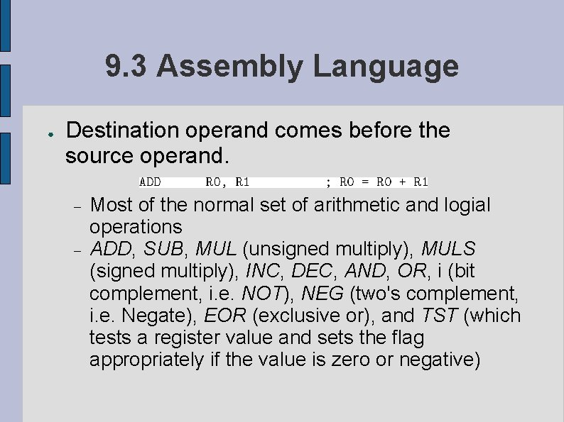
9. 3 Assembly Language ● Destination operand comes before the source operand. Most of the normal set of arithmetic and logial operations ADD, SUB, MUL (unsigned multiply), MULS (signed multiply), INC, DEC, AND, OR, i (bit complement, i. e. NOT), NEG (two's complement, i. e. Negate), EOR (exclusive or), and TST (which tests a register value and sets the flag appropriately if the value is zero or negative)

9. 3 Assembly Language ● The slow and expensive division operation is not available, nor is the modulus operator, or any kind of floating point support. -I (SUBI, ORI, ANDI) take an immediate mode constant and perform that operation to the register. Operations on individual bits, SBR (set bit(s) in register) or CBI (clear bit in I/O register).

9. 3 Assembly Language ● Wide range of branch/jump instructions JMP BR? ? ● Jumps based on different flags combinations in the SREG register. CALL SR? ? ● First Letter ● Second letter R (general-purpose register) or an I (I/O register), C (clear bit) or S (set bit), SBIC=Skip if Bit in I/O register is Clear, bit in the appropriate register is set/clear. Indirect jumps IJMP, ICALL

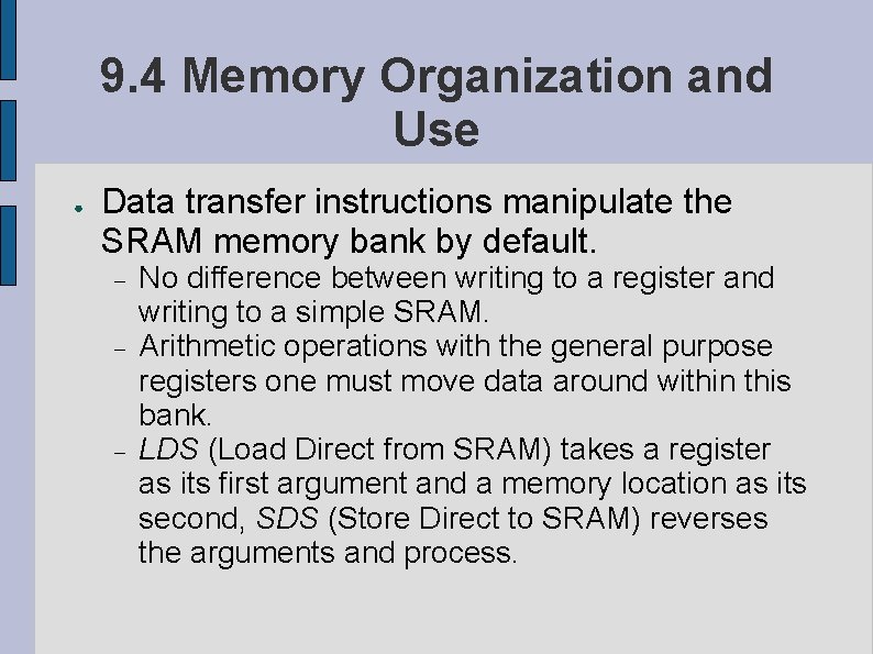
9. 4 Memory Organization and Use ● Data transfer instructions manipulate the SRAM memory bank by default. No difference between writing to a register and writing to a simple SRAM. Arithmetic operations with the general purpose registers one must move data around within this bank. LDS (Load Direct from SRAM) takes a register as its first argument and a memory location as its second, SDS (Store Direct to SRAM) reverses the arguments and process.

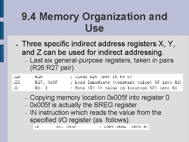
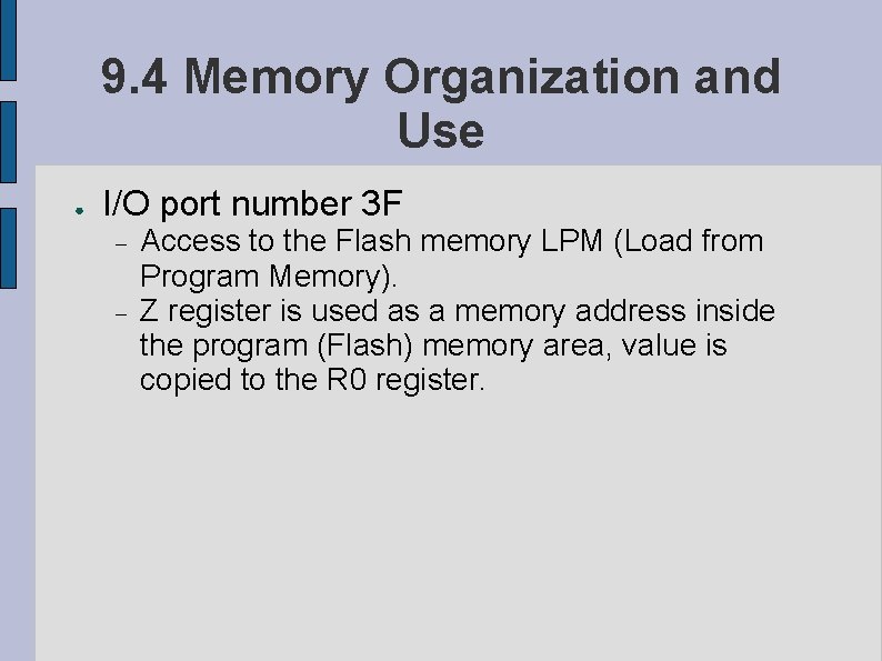
9. 4 Memory Organization and Use ● Three specific indirect address registers X, Y, and Z can be used for indirect addressing. Last six general-purpose registers, taken in pairs (R 26: R 27 pair) Copying memory location 0 x 005 f into register 0. 0 x 005 f is actually the SREG register IN instruction which reads the value from the specified I/O register (as follows).

9. 4 Memory Organization and Use ● I/O port number 3 F Access to the Flash memory LPM (Load from Program Memory). Z register is used as a memory address inside the program (Flash) memory area, value is copied to the R 0 register.

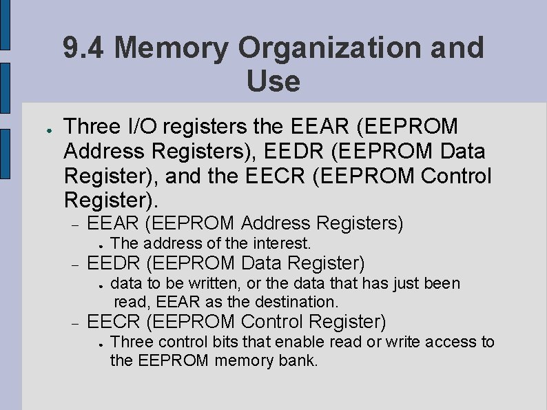
9. 4 Memory Organization and Use ● Three I/O registers the EEAR (EEPROM Address Registers), EEDR (EEPROM Data Register), and the EECR (EEPROM Control Register). EEAR (EEPROM Address Registers) ● EEDR (EEPROM Data Register) ● The address of the interest. data to be written, or the data that has just been read, EEAR as the destination. EECR (EEPROM Control Register) ● Three control bits that enable read or write access to the EEPROM memory bank.

9. 4 Memory Organization and Use ● Read from a given location in the EEPROM. Bit 0 ● EERE (EEPROM Read Enable) bit Load the byte address of interest into the EEAR. Set the EERE set to 1, allowing the read to proceed. After the read operation completes, the relevant data can be found in the EEDR.

9. 4 Memory Organization and Use ● Write two enabling bits that need to be set. Bit 2 ● EEMWE (EEPROM Master Write Enable) bit; when set to 1, t he CPU is “enabled” to write th EEPROM. Actual writing is performed by setting bit 1 (the EEWE/EEPROM Write Enable) bit to 1 after the EEMWE has also been set to 1. EEMWE will automatically be returned to 0 after a short period of time.

9. 4 Memory Organization and Use ● Write to the EEPROM: ● Load the byte address of interest into the EEAR. Load the new data into the EEDR. Set the EEMWE to 1, enabling writing to the EEPROM bank. (within four clock cycles) set the EEWE to 1, allowing the write actually to happen. Slow takes as much as 4 ms. A chip running at 10 MHz enough time to perform 40, 000(!) other operations.

9. 5. 1 Interfacing With External Devices. ● Each device is controlled (and interacted with) through a small set of defined registers in the I/O register bank. AT 90 S 2313 provided as a UART attached to a set of pins configured to drive a standard serial port. CPU interacts with the UART hardware through a set of four registers, the UART I/O Data Register, UART Control Register, the UART Band Rate Register, the UART Status register.

9. 5. 1 Interfacing With External Devices. ● Sending data across the UART The UART I/O data register must first be loaded with the data to be transmitted, the Band Rate Register must be loaded with a pattern representing the desired speed. The control register must be set to “Transmitter Enable”. Error transmission, appropriate bits will be set in the Status register where the computer can observe them and take appropriate corrective action.

9. 5. 1 Interfacing With External Devices. ● Data ports are configured to allow up to eight independent electrical signals to be transferred simultaneously. Each data port is controlled by two registers ● Data Direction Register ● Each individual bit controls an input or output device Data Register Holds the appropriate value.

9. 5. 2 Interfacing with Timers ● Conceptually, these timers are very simple. Set to an initial value. The time counts clock pulses, either from the internal system clock or an external source of timing pulses, until the internal register “rolls over” by counting from a set of all ones to a set of all zeros. The timer goes off and the appropriate amount of time has passed.

9. 5. 2 Interfacing with Timers ● Example: pulses every 2 microseconds. Initial value of 6. After 250 increments (500 microseconds, or about 1/2000 of a second) the timer will “roll over” to 256, which will overflow the register to 0. The timer can somehow signal the CPU that an appropriate amount of time has passed so the CPU can do whatever it was waiting for.

9. 5. 2 Interfacing with Timers ● Watchdog timer prevent the system from locking up. Toaster program could have a bug that went into an infinite loop right after the heating element turned on. Watchdog works as a normal timer, except that the “signals” it sends the CPU are equivalent to pressing the reset button and thus restarting the system in a known (sane) state.

9. 5. 2 Interfacing with Timers ● Two ways that the CPU can interact with the timer. CPU puts itself into a loop, polling the appropriate I/O register to see whether or not the time has completed. ● Prevents the CPU from getting any other, more useful, processing accomplished. Set up an interrupt handler. ● AVR knows a few very general kinds of interrupts that are generated under hardware-defined circumstances, such as the timer overflowing.

9. 5. 2 Interfacing with Timers Interrupts number from zero to a small value (like ten). Correspond to locations in Flash ROM in the interrupt vector. All that is stored in the actual interrupt location itself is a single JMP instruction to transfer control. ● The watchdog timer is defined to generate the same interrupt that would be created by the reset button or a power-on event.

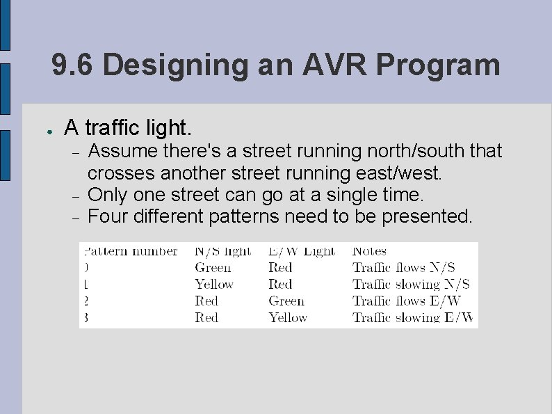
9. 6 Designing an AVR Program ● A traffic light. Assume there's a street running north/south that crosses another street running east/west. Only one street can go at a single time. Four different patterns need to be presented.

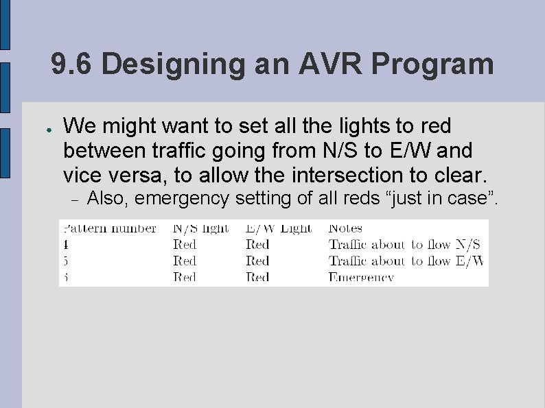
9. 6 Designing an AVR Program ● We might want to set all the lights to red between traffic going from N/S to E/W and vice versa, to allow the intersection to clear. Also, emergency setting of all reds “just in case”.

9. 6 Designing an AVR Program ● Patterns in the following order: 0, 1, 5, 2, 3, 4, 0, . . ● No real stopping point for the program. Essential that the program run in an infinite loop. State machine “state” of such a program is simply a number representing what pattern the lights are currently displaying. Each state can be held for a certain length of time. ● When the timer interrupt occurs, it changes the “state” (and the lights) and reset the timer.

9. 6 Designing an AVR Program ● Make use of other interrupts in this state table. Police-only switch to a pin corresponding to an external interrupt. All red emergency state. ● ● ● The controller will immediately execute the interrupt. Detect when/if a passing pedestrian presses the “walk” button. Watchdog timer to look for possible program bugs, kicking it as necessary, we could either have the program go to a specific pre-programmed normal state, or else to got the “emergency” state on the grounds that something had to have gone wrong.

9. 7 Chapter Review ● ● Microcontroller is a small, single-chip, limitedcapacity computer used for small scale operations such as device control or monitoring. Found in many kinds of gadgets and devices, most of which wouldn't seem (offhand) to be computers at all.

9. 7 Chapter Review ● The architecture of the AVR is substantially different from the architecture of a more typical full-service computer. ● ● Doesn't have support for floating point operations, contains fewer than 10, 000 bytes of memory, but has extensive on-board peripheral device support. AVR is an example of RISC processing. AVR is an example of Harvard architecture, memory is divided into several (in this case, three) different banks.

9. 7 Chapter Review ● ● Input and output in the Atmel AVR is accomplished through I/O registers in the memory bank. Infrequent but expected events are handled efficiently using an interrupts and its corresponding interrupt handler.

9. 7 Chapter Review ● Only a good chip for certain kinds of programs due to the limitations of its hardware and capacities. A typical microcontroller program is a state machine that simply runs forever performing a well-defined set of actions in a fixed, predefined sequence.