Chapter 9 I 2 C Protocol and RTC
![DATA Register Bits 7 -0 Field DATA[7: 0] Description Data The master data register DATA Register Bits 7 -0 Field DATA[7: 0] Description Data The master data register](https://slidetodoc.com/presentation_image/70d3f16a139a4226bf3298fdc0ab6538/image-25.jpg)
- Slides: 39

Chapter 9 I 2 C Protocol and RTC Interfacing 1

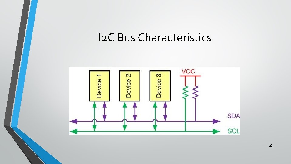
I 2 C Bus Characteristics 2

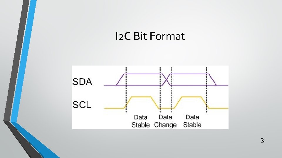
I 2 C Bit Format 3

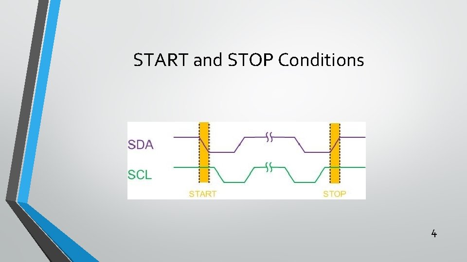
START and STOP Conditions 4

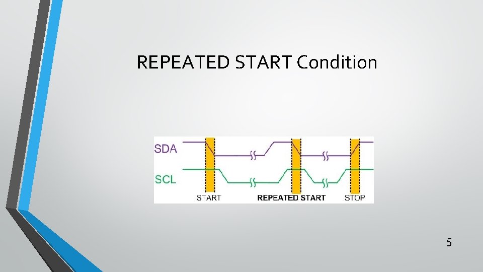
REPEATED START Condition 5

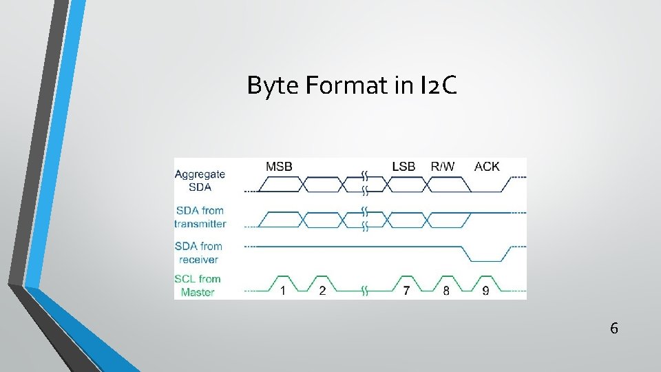
Byte Format in I 2 C 6

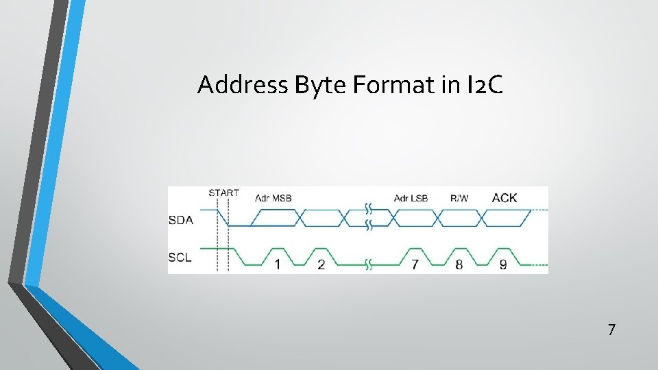
Address Byte Format in I 2 C 7

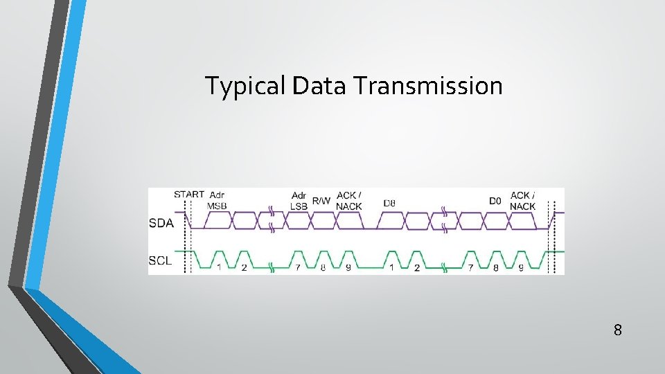
Typical Data Transmission 8

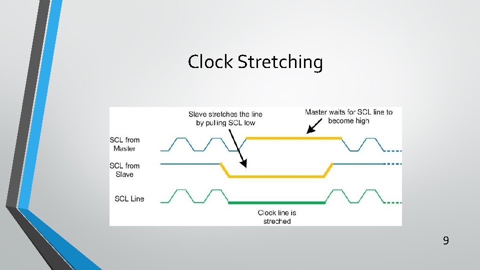
Clock Stretching 9

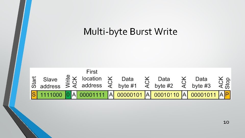
Multi-byte Burst Write 10

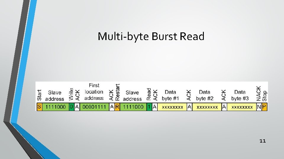
Multi-byte Burst Read 11

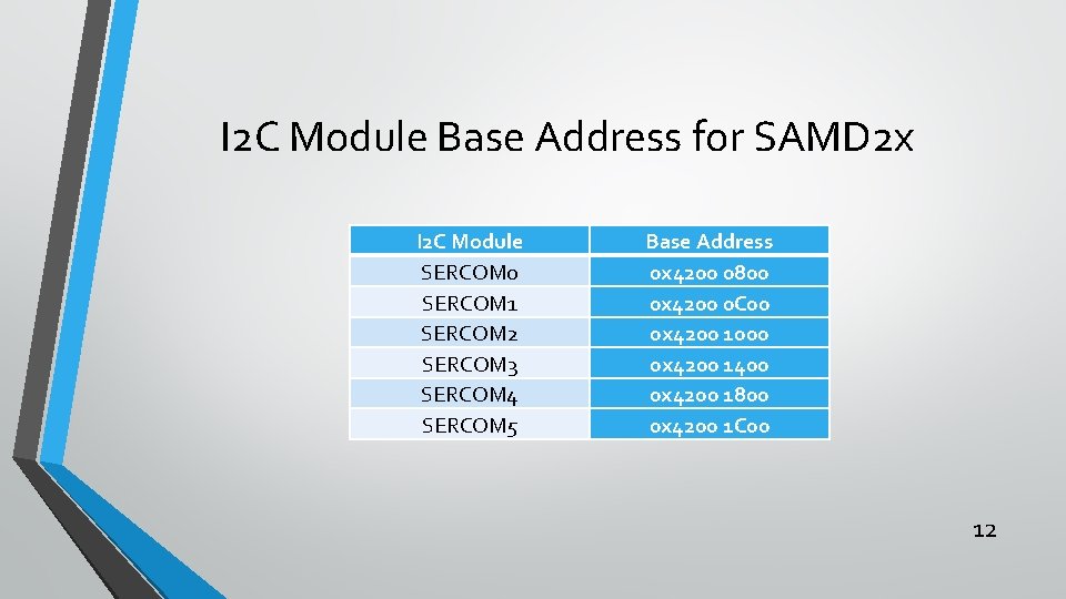
I 2 C Module Base Address for SAMD 2 x I 2 C Module SERCOM 0 SERCOM 1 SERCOM 2 SERCOM 3 SERCOM 4 SERCOM 5 Base Address 0 x 4200 0800 0 x 4200 0 C 00 0 x 4200 1000 0 x 4200 1400 0 x 4200 1800 0 x 4200 1 C 00 12

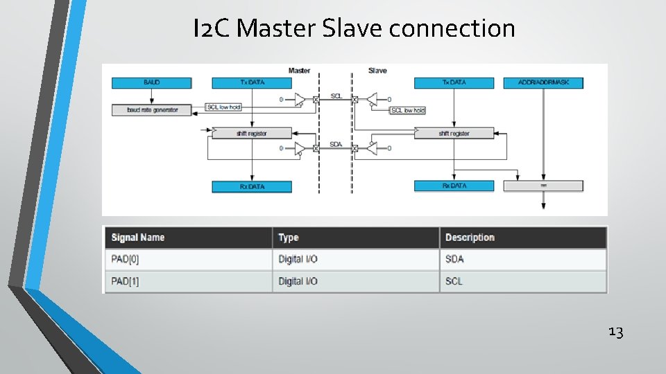
I 2 C Master Slave connection 13

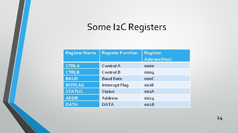
Some I 2 C Registers Register Name Register Function CTRLA CTRLB BAUD INTFLAG STATUS ADDR DATA Control B Baud Rate Interrupt Flag Status Address DATA Register Address(Hex) 0000 0004 000 C 0018 001 A 0024 0028 14

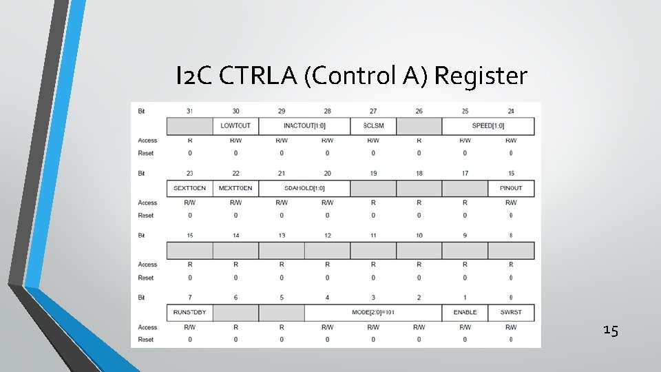
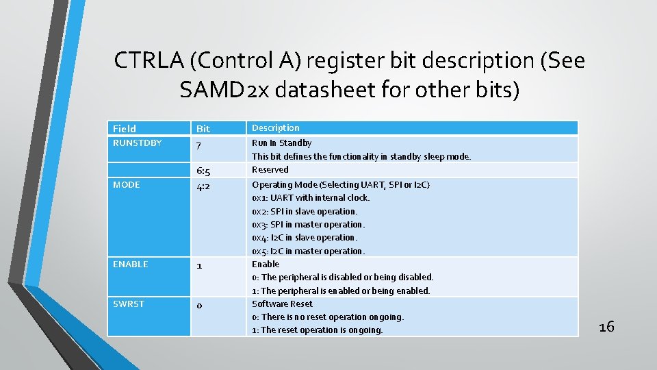
I 2 C CTRLA (Control A) Register 15

CTRLA (Control A) register bit description (See SAMD 2 x datasheet for other bits) Field RUNSTDBY Bit 7 MODE 6: 5 4: 2 ENABLE 1 SWRST 0 Description Run In Standby This bit defines the functionality in standby sleep mode. Reserved Operating Mode (Selecting UART, SPI or I 2 C) 0 x 1: UART with internal clock. 0 x 2: SPI in slave operation. 0 x 3: SPI in master operation. 0 x 4: I 2 C in slave operation. 0 x 5: I 2 C in master operation. Enable 0: The peripheral is disabled or being disabled. 1: The peripheral is enabled or being enabled. Software Reset 0: There is no reset operation ongoing. 1: The reset operation is ongoing. 16

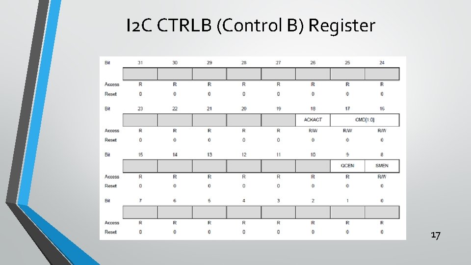
I 2 C CTRLB (Control B) Register 17

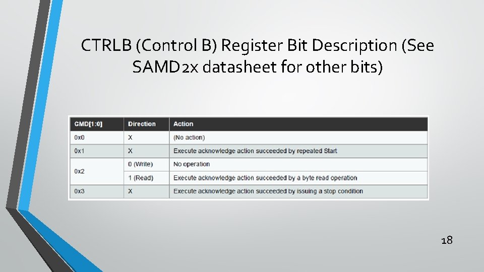
CTRLB (Control B) Register Bit Description (See SAMD 2 x datasheet for other bits) 18

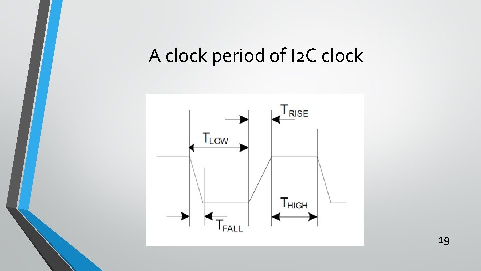
A clock period of I 2 C clock 19

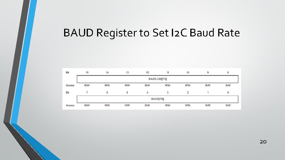
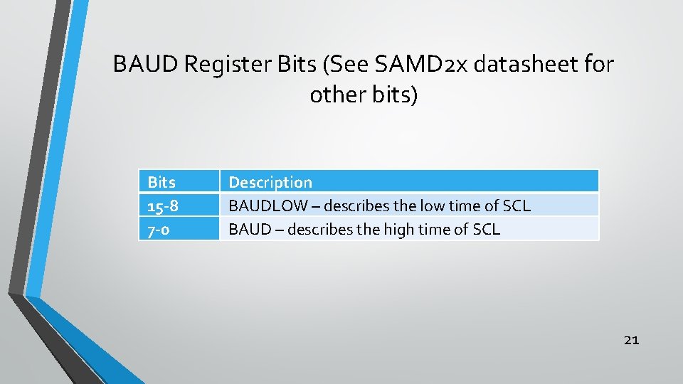
BAUD Register to Set I 2 C Baud Rate 20

BAUD Register Bits (See SAMD 2 x datasheet for other bits) Bits 15 -8 7 -0 Description BAUDLOW – describes the low time of SCL BAUD – describes the high time of SCL 21

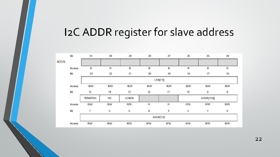
I 2 C ADDR register for slave address 22

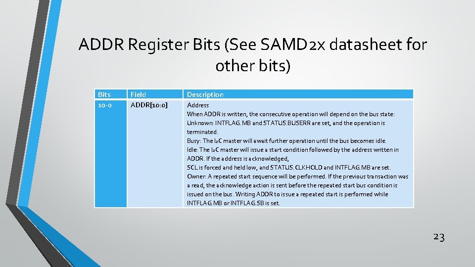
ADDR Register Bits (See SAMD 2 x datasheet for other bits) Bits 10 -0 Field ADDR[10: 0] Description Address When ADDR is written, the consecutive operation will depend on the bus state: Unknown: INTFLAG. MB and STATUS. BUSERR are set, and the operation is terminated. Busy: The I 2 C master will await further operation until the bus becomes idle. Idle: The I 2 C master will issue a start condition followed by the address written in ADDR. If the address is acknowledged, SCL is forced and held low, and STATUS. CLKHOLD and INTFLAG. MB are set. Owner: A repeated start sequence will be performed. If the previous transaction was a read, the acknowledge action is sent before the repeated start bus condition is issued on the bus. Writing ADDR to issue a repeated start is performed while INTFLAG. MB or INTFLAG. SB is set. 23

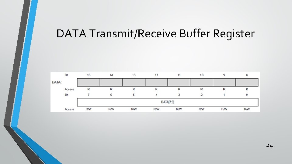
DATA Transmit/Receive Buffer Register 24
![DATA Register Bits 7 0 Field DATA7 0 Description Data The master data register DATA Register Bits 7 -0 Field DATA[7: 0] Description Data The master data register](https://slidetodoc.com/presentation_image/70d3f16a139a4226bf3298fdc0ab6538/image-25.jpg)
DATA Register Bits 7 -0 Field DATA[7: 0] Description Data The master data register I/O location (DATA) provides access to the master transmit and receive data buffers. Reading valid data or writing data to be transmitted can be successfully done only when SCL is held low by the master (STATUS. CLKHOLD is set). An exception occurs when reading the last data byte after the stop condition has been sent. 25

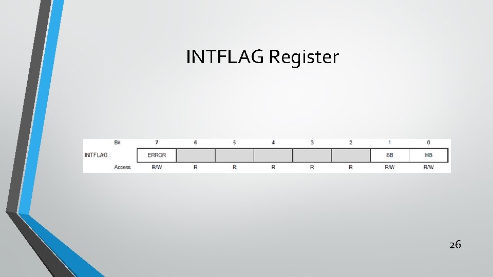
INTFLAG Register 26

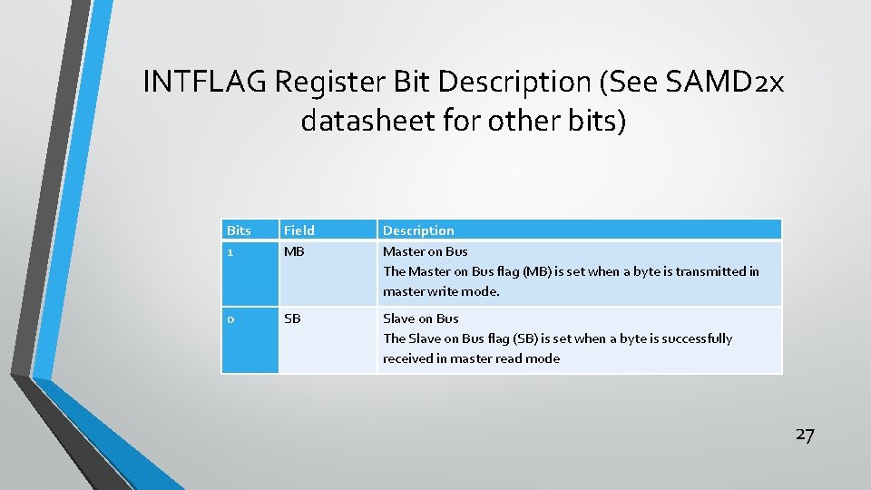
INTFLAG Register Bit Description (See SAMD 2 x datasheet for other bits) Bits 1 Field MB Description Master on Bus The Master on Bus flag (MB) is set when a byte is transmitted in master write mode. 0 SB Slave on Bus The Slave on Bus flag (SB) is set when a byte is successfully received in master read mode 27

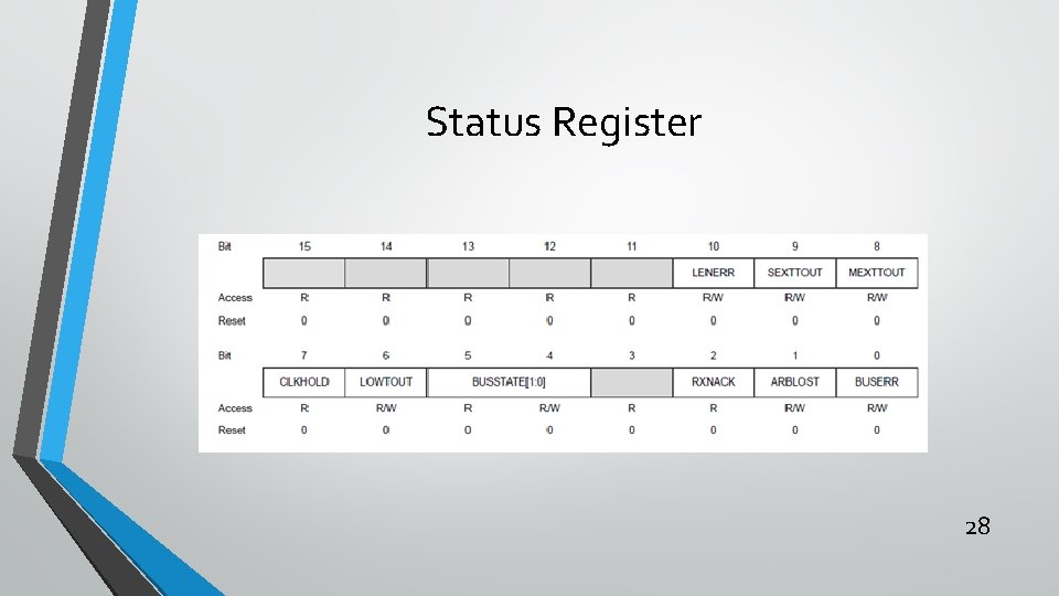
Status Register 28

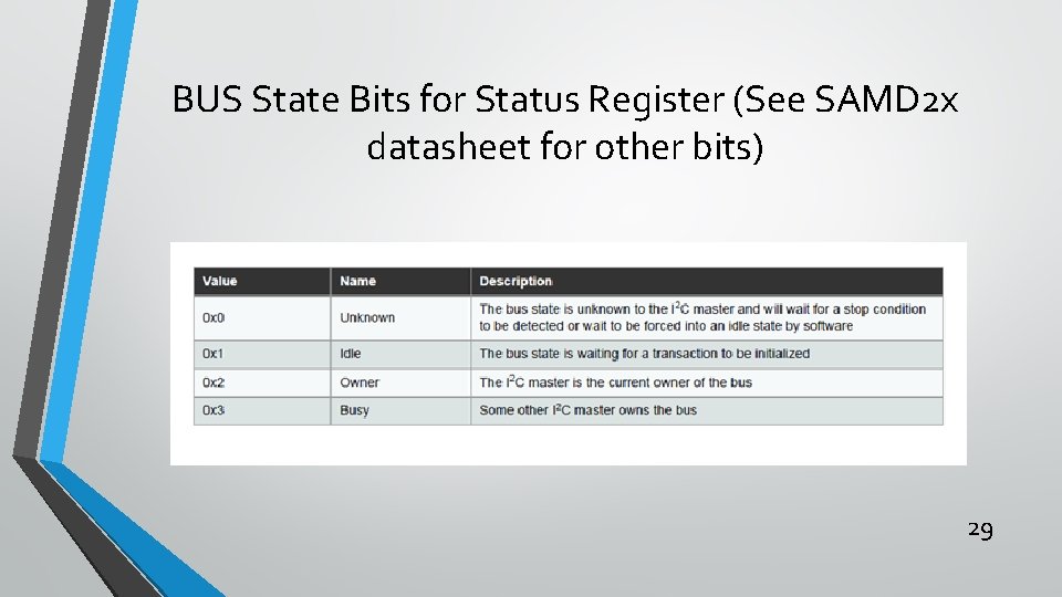
BUS State Bits for Status Register (See SAMD 2 x datasheet for other bits) 29

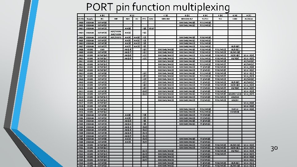
PORT pin function multiplexing A (0) C (2) D (3) E (4) F (5) G (6) H (7) I/O Pin Supply EIC REF ADC B (1) AC PTC DAC SERCOM-ALT TC/TCC COM AC/GCLK PA 00 PA 01 PA 02 VDDANA EXTINT[0] EXTINT[1] EXTINT[2] AIN[0] Y[0] VOUT SERCOM 1/PAD[0] SERCOM 1/PAD[1] TCC 2/WO[0] TCC 2/WO[1] PA 03 VDDANA EXTINT[3] AIN[1] Y[1] PA 04 PA 05 PA 06 PA 07 PA 08 PA 09 PA 10 PA 11 PA 12 PA 13 PA 14 PA 15 PA 16 PA 17 PA 18 PA 19 PA 20 PA 21 PA 22 PA 23 PA 24 PA 25 PA 27 PA 28 PA 30 PA 31 PB 00 PB 01 PB 02 PB 03 PB 04 PB 05 PB 06 PB 07 PB 08 PB 09 PB 10 PB 11 PB 12 PB 13 PB 14 PB 15 PB 16 PB 17 VDDANA VDDIO VDDIO VDDIO VDDIO VDDIO VDDIO VDDANA VDDANA VDDANA VDDIO VDDIO EXTINT[4] EXTINT[5] EXTINT[6] EXTINT[7] NMI EXTINT[9] EXTINT[10] EXTINT[11] EXTINT[12] EXTINT[13] EXTINT[14] EXTINT[15] EXTINT[0] EXTINT[1] EXTINT[2] EXTINT[3] EXTINT[4] EXTINT[5] EXTINT[6] EXTINT[7] EXTINT[12] EXTINT[13] EXTINT[15] EXTINT[8] EXTINT[10] EXTINT[11] EXTINT[0] EXTINT[1] EXTINT[2] EXTINT[3] EXTINT[4] EXTINT[5] EXTINT[6] EXTINT[7] EXTINT[8] EXTINT[9] EXTINT[10] EXTINT[11] EXTINT[12] EXTINT[13] EXTINT[14] EXTINT[15] EXTINT[0] EXTINT[1] ADC/VREFA DAC/VREFA ADC/VREFB AIN[4] AIN[5] AIN[6] AIN[7] AIN[16] AIN[17] AIN[18] AIN[19] AIN[8] AIN[9] AIN[10] AIN[11] AIN[12] AIN[13] AIN[14] AIN[15] AIN[2] AIN[3] AIN[0] AIN[1] AIN[2] AIN[3] Y[2] Y[3] Y[4] Y[5] X[0] X[1] X[2] X[3] X[4] X[5] X[6] X[7] X[8] X[9] X[10] X[11] Y[6] Y[7] Y[8] Y[9] Y[10] Y[11] Y[12] Y[13] Y[14] Y[15] X[12] X[13] X[14] X[15] SERCOM 0/PAD[0] SERCOM 0/PAD[1] SERCOM 0/PAD[2] SERCOM 0/PAD[3] SERCOM 2/PAD[0] SERCOM 2/PAD[1] SERCOM 2/PAD[2] SERCOM 2/PAD[3] SERCOM 1/PAD[0] SERCOM 1/PAD[1] SERCOM 1/PAD[2] SERCOM 1/PAD[3] SERCOM 5/PAD[2] SERCOM 5/PAD[3] SERCOM 3/PAD[0] SERCOM 3/PAD[1] SERCOM 3/PAD[2] SERCOM 3/PAD[3] SERCOM 4/PAD[0] SERCOM 4/PAD[1] SERCOM 4/PAD[2] SERCOM 4/PAD[3] SERCOM 5/PAD[0] SERCOM 5/PAD[1] SERCOM 0/PAD[0] SERCOM 0/PAD[1] SERCOM 0/PAD[2] SERCOM 0/PAD[3] SERCOM 2/PAD[0] SERCOM 2/PAD[1] SERCOM 2/PAD[2] SERCOM 2/PAD[3] SERCOM 4/PAD[0] SERCOM 4/PAD[1] SERCOM 4/PAD[2] SERCOM 4/PAD[3] SERCOM 3/PAD[0] SERCOM 3/PAD[1] SERCOM 3/PAD[2] SERCOM 3/PAD[3] SERCOM 5/PAD[0] SERCOM 5/PAD[1] SERCOM 5/PAD[2] SERCOM 5/PAD[3] SERCOM 1/PAD[2] SERCOM 1/PAD[3] SERCOM 5/PAD[2] SERCOM 5/PAD[3] SERCOM 5/PAD[0] SERCOM 5/PAD[1] SERCOM 4/PAD[0] SERCOM 4/PAD[1] SERCOM 4/PAD[2] SERCOM 4/PAD[3] TCC 0/WO[0] TCC 0/WO[1] TCC 1/WO[0] TCC 1/WO[1] TCC 2/WO[0] TCC 2/WO[1] TC 3/WO[0] TC 3/WO[1] TC 7/WO[0] TC 7/WO[1] TC 4/WO[0] TC 4/WO[1] TC 5/WO[0] TC 5/WO[1] TCC 1/WO[0] TCC 1/WO[1] TC 7/WO[0] TC 7/WO[1] TC 6/WO[0] TC 6/WO[1] TC 4/WO[0] TC 4/WO[1] TC 5/WO[0] TC 5/WO[1] TC 6/WO[0] TC 6/WO[1] TCC 1/WO[2] TCC 1/WO[3] TCC 0/WO[2] TCC 0/WO[3] TCC 0/WO[6] TCC 0/WO[7] TCC 0/WO[4] TCC 0/WO[5] TCC 0/WO[6] TCC 0/WO[7] TCC 0/WO[2] TCC 0/WO[3] TCC 0/WO[6] TCC 0/WO[7] TCC 0/WO[4] TCC 0/WO[5] TCC 1/WO[2] TCC 1/WO[3] TCC 0/WO[4] TCC 0/WO[5] TCC 0/WO[6] TCC 0/WO[7] TCC 0/WO[4] TCC 0/WO[5] I 2 S/SD[0] I 2 S/SD[1] I 2 S/MCK[0] I 2 S/SCK[0] I 2 S/FS[0] I 2 S/SD[0] I 2 S/SCK[0] I 2 S/FS[0] USB/SOF 1 k. Hz USB/DM USB/DP SWCLK SWDIO(4) I 2 S/MCK[1] I 2 S/SCK[1] I 2 S/FS[1] I 2 S/SD[1] I 2 S/MCK[0] GCLK_IO[4] GCLK_IO[5] AC/CMP[0] AC/CMP[1] GCLK_IO[0] GCLK_IO[1] GCLK_IO[2] GCLK_IO[3] AC/CMP[0] AC/CMP[1] GCLK_IO[4] GCLK_IO[5] GCLK_IO[6] GCLK_IO[7] GCLK_IO[0] GCLK_IO[4] GCLK_IO[5] GCLK_IO[6] GCLK_IO[7] GCLK_IO[0] GCLK_IO[1] GCLK_IO[2] GCLK_IO[3] 30

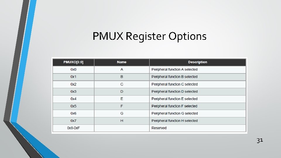
PMUX Register Options 31

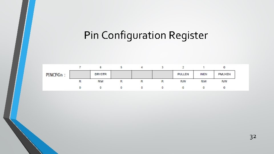
Pin Configuration Register 32

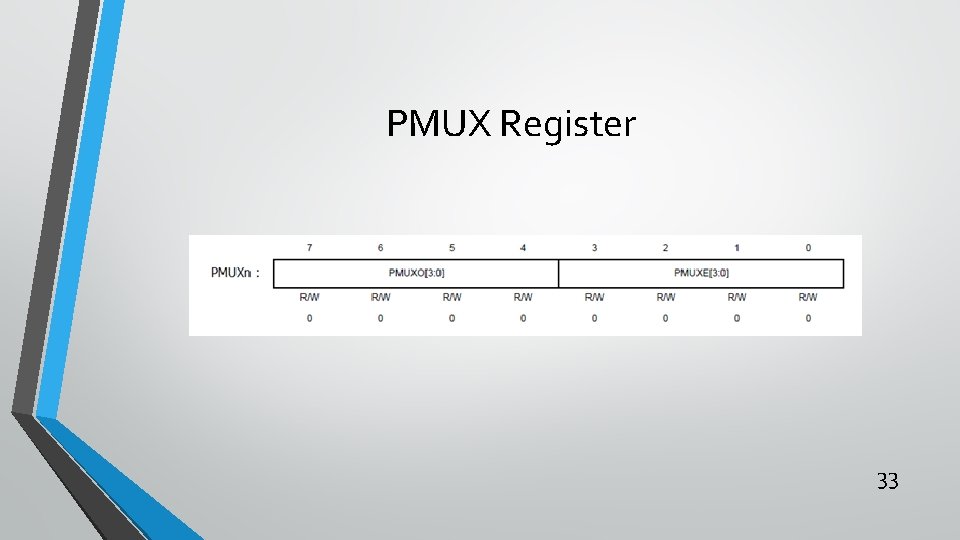
PMUX Register 33

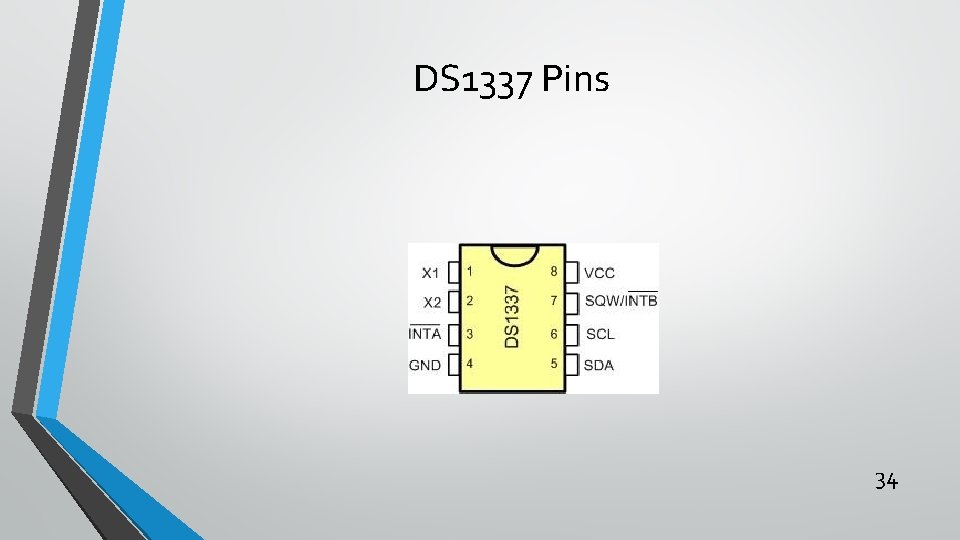
DS 1337 Pins 34

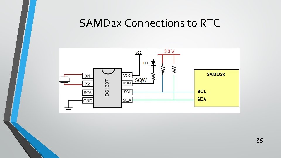
SAMD 2 x Connections to RTC 35

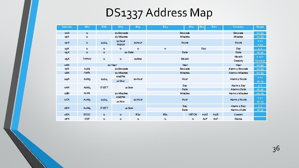
DS 1337 Address Map Address Bit 7 Bit 6 Bit 5 00 H 01 H 0 0 02 H 0 12/24 03 H 04 H 0 0 05 H Century 0 0 Bit 4 10 Seconds 10 Minutes 10 hour Bit 3 10 hour PM/AM 0 Function Range Seconds Minutes Hours Day Date 00 -59 1 -12 0 -23 0 -7 01 -31 Month Century 1 -12+ Century Year Seconds Minutes Year Alarm 1 Seconds Alarm 1 Minutes 00 -99 00 -59 Hour Alarm 1 Hours 1 -12 00 -23 Day Date Minutes Alarm 1 Day Alarm 1 Date Alarm 2 Minutes 1 -7 01 -31 00 -59 Hour Alarm 2 Hours 1 -12 00 -23 Day Date Alarm 2 Day Alarm 2 Date 1 -7 01 -31 0 10 Date Bit 1 Bit 0 Day Date 10 Mnt 06 H 07 H 08 H A 1 M 2 09 H A 1 M 3 12/24 0 AH A 1 M 4 DY/DT 0 BH A 2 M 2 0 CH A 2 M 3 12/24 0 DH A 2 M 4 DY/DT 0 EH EOSC 0 0 RS 2 RS 1 INTCN A 2 IE A 1 IE Control - 0 FH OSF 0 0 0 A 2 F A 1 F Status - A 1 M 1 10 Year 10 Seconds 10 Minutes AM/PM Bit 2 10 Hour 10 Date 10 Minutes AM/PM 10 Hour 10 Date 36

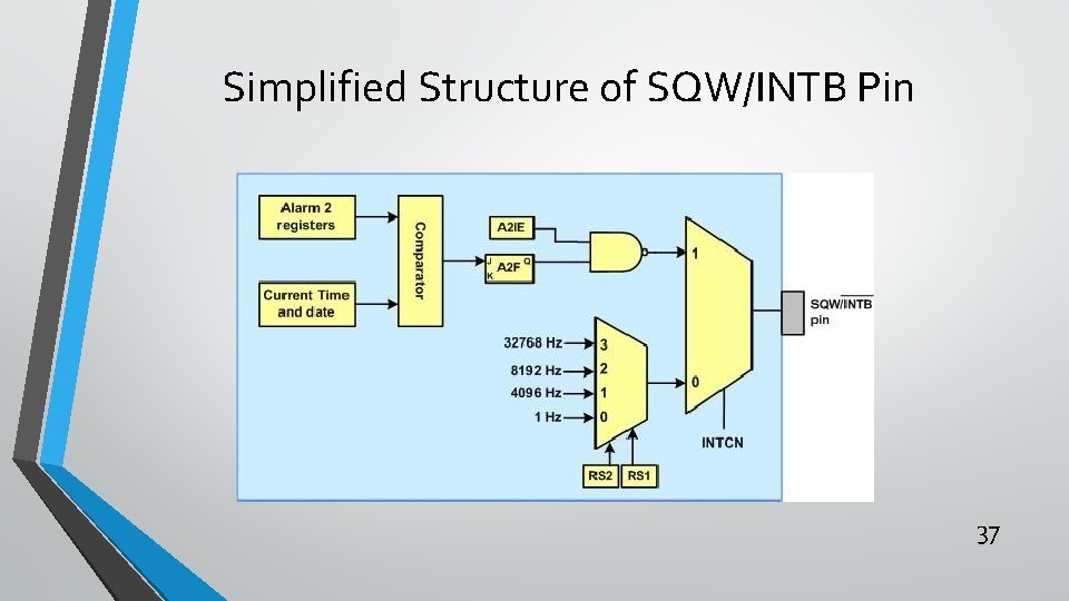
Simplified Structure of SQW/INTB Pin 37

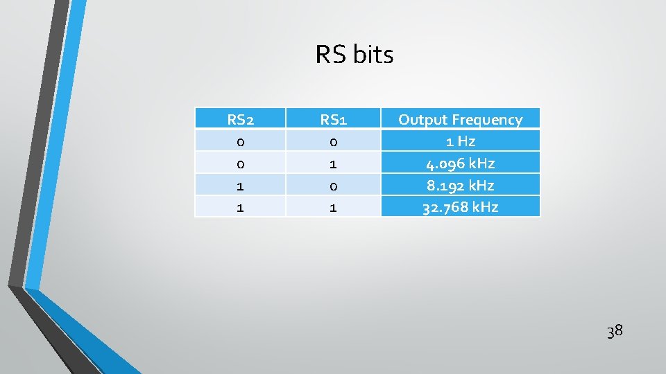
RS bits RS 2 0 0 1 1 RS 1 0 1 Output Frequency 1 Hz 4. 096 k. Hz 8. 192 k. Hz 32. 768 k. Hz 38

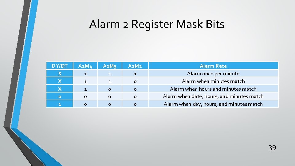
Alarm 2 Register Mask Bits DY/DT X X X 0 1 A 2 M 4 1 1 1 0 0 A 2 M 3 1 1 0 0 0 A 2 M 2 1 0 0 Alarm Rate Alarm once per minute Alarm when minutes match Alarm when hours and minutes match Alarm when date, hours, and minutes match Alarm when day, hours, and minutes match 39